

How to Optimize EUV Lithography Wafer Throughput
APR 2, 20268 MIN READ
Generate Your Research Report Instantly with AI Agent
Patsnap Eureka helps you evaluate technical feasibility & market potential.
EUV Lithography Development Background and Throughput Goals
Extreme Ultraviolet (EUV) lithography represents a revolutionary advancement in semiconductor manufacturing, emerging as the critical technology for producing advanced nodes below 7nm. The development of EUV lithography began in the 1980s as a collaborative effort between government laboratories, research institutions, and industry partners, driven by the fundamental physical limitations of traditional optical lithography systems. As Moore's Law continued to demand smaller feature sizes, conventional 193nm immersion lithography reached its practical limits, necessitating a paradigm shift to shorter wavelengths.
The transition to EUV technology utilizing 13.5nm wavelength light has been one of the most challenging technological endeavors in semiconductor history. Initial research focused on overcoming fundamental physics challenges including light source power, mask defectivity, and resist sensitivity. The technology required unprecedented precision in manufacturing and metrology, with tolerances measured in picometers and femtoseconds.
ASML emerged as the sole supplier of EUV lithography systems after decades of development and billions of dollars in investment. The first production-worthy EUV systems, the NXE:3400 series, achieved commercial viability around 2017-2018, marking a critical milestone in semiconductor manufacturing capability. However, early systems suffered from significant throughput limitations, with productivity rates far below the industry requirements for high-volume manufacturing.
Current throughput optimization goals center on achieving sustainable production rates exceeding 185 wafers per hour, representing a substantial improvement from early systems that struggled to reach 125 wafers per hour. The industry roadmap targets further enhancements to support the economic viability of EUV lithography for high-volume manufacturing across multiple technology nodes.
Key throughput objectives include maximizing source power utilization, minimizing downtime through predictive maintenance, optimizing exposure strategies, and enhancing overall equipment effectiveness. These goals directly impact the total cost of ownership and determine the commercial feasibility of EUV adoption across different market segments.
The semiconductor industry's commitment to EUV throughput optimization reflects the technology's critical role in enabling continued scaling and performance improvements in advanced processors, memory devices, and emerging applications requiring cutting-edge semiconductor capabilities.
Market Demand for High-Volume EUV Manufacturing
The semiconductor industry faces unprecedented demand for advanced node manufacturing capabilities, with EUV lithography serving as the critical enabler for producing chips at 7nm and below. Major foundries including TSMC, Samsung, and Intel have committed substantial capital investments to expand their EUV manufacturing capacity, driven by surging demand from artificial intelligence, high-performance computing, and mobile processor markets.
Current market dynamics reveal a significant bottleneck in EUV production capacity relative to customer demand. Leading foundries report order backlogs extending beyond traditional planning horizons, with premium pricing sustained across advanced node processes. The limited availability of EUV scanners from ASML, combined with their complex operational requirements, creates a supply-demand imbalance that directly correlates with wafer throughput optimization needs.
Automotive semiconductor demand adds another layer of complexity, as the industry transitions toward electric vehicles and autonomous driving systems requiring advanced processing capabilities. These applications demand both high-volume production and stringent quality standards, placing additional pressure on EUV manufacturing efficiency. The geopolitical landscape further intensifies market demand, with regional semiconductor independence initiatives driving domestic capacity expansion across multiple geographic markets.
Cloud computing infrastructure expansion continues accelerating, fueled by artificial intelligence workloads requiring cutting-edge processors manufactured using EUV technology. Data center operators increasingly specify advanced node chips for energy efficiency and performance advantages, creating sustained demand pressure on foundry capacity. This trend shows no signs of abating as machine learning applications proliferate across industries.
The economic value proposition of throughput optimization becomes evident when considering EUV scanner capital costs and operational expenses. Each percentage point improvement in wafer throughput directly translates to enhanced return on investment for foundry operators, making optimization technologies highly attractive. Market research indicates that foundries prioritize throughput enhancement solutions that can deliver measurable capacity increases without compromising yield or quality standards.
Emerging applications in quantum computing, advanced packaging, and next-generation memory technologies promise to sustain long-term demand for EUV manufacturing capacity. These markets represent additional growth vectors beyond traditional logic and memory segments, reinforcing the strategic importance of maximizing existing EUV infrastructure productivity through advanced throughput optimization techniques.
Current EUV Throughput Limitations and Technical Challenges
EUV lithography systems currently face significant throughput limitations that constrain their widespread adoption in high-volume manufacturing. The primary bottleneck stems from the inherently low power output of EUV light sources, which typically operate at 250-300 watts, far below the theoretical requirements for optimal productivity. This power limitation directly translates to extended exposure times, reducing the number of wafers that can be processed per hour.
Source availability represents another critical challenge, as EUV systems require extremely stable and consistent light generation. Current laser-produced plasma sources suffer from debris generation and tin contamination, necessitating frequent maintenance cycles that interrupt production flow. The conversion efficiency from input laser power to usable EUV photons remains below 5%, creating substantial energy waste and thermal management issues.
Resist sensitivity poses additional throughput constraints, as current photoresist materials require higher photon doses to achieve adequate pattern fidelity. The stochastic effects inherent in EUV exposure, including photon shot noise and resist molecular interactions, demand increased exposure doses to maintain acceptable defect levels, further extending processing times.
Mask-related challenges significantly impact system productivity. EUV masks are susceptible to contamination and defect growth during exposure, requiring frequent cleaning cycles and replacement. The pellicle-free operation of EUV systems makes masks vulnerable to particle contamination, leading to yield losses and additional inspection overhead.
Thermal management presents ongoing difficulties as the high-power laser systems and plasma sources generate substantial heat loads. Maintaining stable operating temperatures across critical components while managing thermal expansion effects requires sophisticated cooling systems that can limit system availability.
Optical component degradation, particularly of multilayer mirrors, occurs gradually through exposure to EUV radiation and residual gases. This degradation necessitates periodic replacement and recalibration procedures that reduce overall equipment effectiveness and increase operational costs, creating additional barriers to achieving target throughput levels in production environments.
Existing EUV Throughput Optimization Solutions
01 Multi-stage reticle handling and loading systems
Implementation of advanced reticle handling mechanisms that enable parallel processing and reduced reticle exchange time. These systems utilize multi-stage loading configurations, automated reticle libraries, and optimized transport mechanisms to minimize downtime between exposures. The technology includes pre-positioning of reticles and synchronized handoff procedures that allow continuous operation while maintaining alignment accuracy.- Multi-stage reticle handling and loading systems: Implementation of multi-stage reticle handling systems that enable parallel processing of wafer exposure and reticle exchange operations. These systems utilize buffer stages and automated loading mechanisms to minimize reticle exchange time, allowing continuous wafer processing while the next reticle is being prepared. Advanced robotics and positioning systems ensure precise alignment while maintaining high throughput rates.
- Optimized wafer stage scanning and positioning control: Advanced wafer stage control systems that optimize scanning trajectories and acceleration profiles to reduce exposure time per wafer. These systems employ predictive positioning algorithms, dual-stage configurations, and high-speed interferometric measurement systems to achieve faster wafer movement while maintaining nanometer-level accuracy. The optimization includes minimizing settling time and implementing continuous scanning modes.
- Parallel wafer processing and multi-patterning techniques: Methods for increasing throughput through parallel processing architectures and efficient multi-patterning strategies. These approaches include simultaneous processing of multiple wafers at different stages, optimized exposure field sequencing, and advanced stitching techniques that reduce the total number of exposure passes required. Integration of intelligent scheduling algorithms maximizes equipment utilization.
- Enhanced EUV source power and dose control optimization: Technologies focused on maximizing effective EUV light utilization and optimizing exposure dose delivery to reduce per-wafer exposure time. These include advanced collector optics designs, improved plasma generation efficiency, and dynamic dose control systems that adapt to pattern density variations. Thermal management solutions enable sustained high-power operation without throughput degradation.
- Integrated metrology and real-time process control: In-line metrology systems and real-time feedback control mechanisms that reduce measurement overhead and enable faster process adjustments. These systems perform overlay measurements, focus monitoring, and dose verification without removing wafers from the production flow. Predictive maintenance algorithms and automated calibration routines minimize downtime and maintain consistent throughput performance.
02 Wafer stage acceleration and positioning optimization
Advanced wafer stage designs featuring high-acceleration motors, optimized motion profiles, and predictive positioning algorithms to reduce inter-field and inter-wafer movement time. These systems employ lightweight materials, magnetic levitation technology, and advanced control systems to achieve faster settling times and improved positioning accuracy. The technology enables overlapping of wafer movement with exposure operations to maximize throughput.Expand Specific Solutions03 Parallel exposure and multi-beam processing
Techniques for simultaneous exposure of multiple die areas or implementation of multiple exposure beams to increase the effective writing speed. These approaches include beam splitting technologies, multi-patterning strategies, and parallel processing architectures that allow multiple regions of a wafer to be exposed concurrently. The methods also encompass optimized field stitching and synchronized multi-beam control systems.Expand Specific Solutions04 Source power optimization and thermal management
Enhanced light source systems with increased power output, improved duty cycles, and advanced thermal management to sustain higher exposure rates. These technologies include plasma source optimization, collector mirror efficiency improvements, and cooling systems that enable continuous high-power operation. The innovations also cover power delivery stabilization and source lifetime extension methods that support sustained high-throughput production.Expand Specific Solutions05 Predictive maintenance and real-time process control
Integration of advanced sensors, machine learning algorithms, and predictive analytics to minimize unplanned downtime and optimize process parameters in real-time. These systems monitor critical components, predict maintenance needs, and automatically adjust exposure parameters to maintain optimal throughput. The technology includes adaptive control systems that compensate for drift and environmental variations while maintaining production efficiency.Expand Specific Solutions
Key Players in EUV Equipment and Process Optimization
The EUV lithography wafer throughput optimization market represents a mature yet rapidly evolving sector within the semiconductor industry, currently valued at several billion dollars and experiencing robust growth driven by advanced node manufacturing demands. The competitive landscape is dominated by established technology leaders across the supply chain. ASML Netherlands BV maintains monopolistic control over EUV lithography systems, while foundry giants Taiwan Semiconductor Manufacturing Co. and Samsung Electronics lead in implementation and optimization. Equipment suppliers like Applied Materials, KLA Corp., and Nikon Corp. provide critical inspection and process control solutions. Memory manufacturers including SK hynix and Nanya Technology drive demand through high-volume production requirements. The technology maturity varies significantly across components, with ASML's EUV systems representing cutting-edge innovation, while supporting infrastructure from companies like Carl Zeiss SMT and specialized materials from Versum Materials demonstrate varying degrees of technological sophistication and market readiness.
Taiwan Semiconductor Manufacturing Co., Ltd.
Technical Solution: TSMC optimizes EUV wafer throughput through advanced fab management and process integration techniques. Their approach focuses on intelligent lot scheduling, multi-patterning reduction strategies, and resist optimization to achieve higher effective throughput. TSMC implements real-time process monitoring with AI-driven defect prediction to minimize rework cycles. They utilize advanced metrology integration and feed-forward control systems to maintain process stability while increasing scan speeds. The company's high-volume manufacturing expertise enables them to achieve industry-leading cycle times through optimized chuck exchange mechanisms, reduced alignment times, and streamlined wafer handling processes that maximize tool utilization rates.
Strengths: Proven high-volume manufacturing expertise and advanced process control capabilities. Weaknesses: Dependent on equipment suppliers for fundamental throughput improvements, limited control over scanner hardware optimization.
ASML Netherlands BV
Technical Solution: ASML leads EUV lithography throughput optimization through advanced scanner architecture and computational lithography solutions. Their latest EXE:5000 series achieves over 185 wafers per hour throughput by implementing high-power EUV sources exceeding 250W, advanced pellicle technology for contamination control, and intelligent scheduling algorithms. The company integrates machine learning-based predictive maintenance to minimize downtime, while their holistic lithography approach combines hardware improvements with software optimization for dose control and overlay accuracy. ASML's co-optimization strategy with resist suppliers and foundries enables faster processing speeds while maintaining critical dimension uniformity across wafers.
Strengths: Market-leading EUV technology with highest throughput rates, comprehensive ecosystem partnerships. Weaknesses: High capital costs and complex maintenance requirements limit accessibility.
Core Technologies for EUV Wafer Processing Acceleration
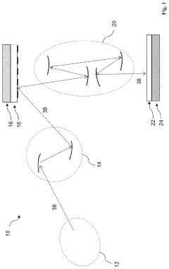
Wafer exposing method, EUV exposing apparatus, and EB exposing apparatus
PatentInactiveUS20090305165A1
Innovation
- A method combining EUV exposure for product areas with EB exposure for peripheral areas, where the EB exposure unit operates concurrently with the EUV exposure unit, using a configuration that allows for efficient EB irradiation of the periphery while maintaining uniform pattern coverage across the wafer.


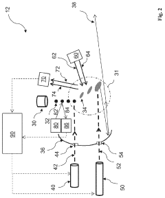
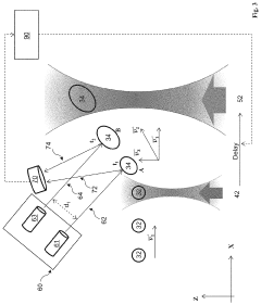
System and Method for Extreme Ultraviolet Source Control
PatentActiveUS20210068241A1
Innovation
- The system employs a dual-pulse laser-produced plasma mechanism with optimized parameters, including pre-pulses and main pulses, to enhance EUV conversion efficiency and minimize debris deposition on the LPP collector by controlling the speed and geometry of target plumes, using a controller to adjust laser pulse energy and timing for optimal EUV radiation generation and collector protection.
EUV Manufacturing Cost Economics and ROI Analysis
EUV lithography represents one of the most capital-intensive manufacturing technologies in semiconductor production, with individual scanner systems costing between $150-200 million. The economic viability of EUV implementation hinges critically on achieving sufficient wafer throughput to justify these substantial investments. Current industry benchmarks indicate that EUV systems must achieve minimum throughput rates of 140-160 wafers per hour to reach acceptable return on investment thresholds for high-volume manufacturing.
The cost structure of EUV manufacturing encompasses several key components that directly impact ROI calculations. Capital equipment costs constitute approximately 60-70% of total ownership expenses, while operational costs including maintenance, consumables, and facility requirements account for the remaining 30-40%. Power consumption alone can reach 1-1.5 MW per scanner, translating to significant ongoing operational expenses that must be factored into long-term economic models.
Throughput optimization directly correlates with improved cost per wafer metrics, creating a multiplicative effect on ROI. Each 10% improvement in throughput can reduce manufacturing costs by 8-12%, assuming fixed overhead allocation. Leading semiconductor manufacturers report that achieving target throughput rates of 185+ wafers per hour enables EUV cost parity with multiple-patterning ArF immersion alternatives for critical layers below 7nm technology nodes.
The economic break-even analysis reveals that EUV systems require minimum utilization rates of 85-90% to achieve positive ROI within typical 5-7 year depreciation cycles. Factors such as source power stability, resist sensitivity improvements, and overlay accuracy enhancements contribute significantly to overall equipment effectiveness and subsequent financial performance.
Manufacturing cost reduction strategies focus on maximizing productive uptime through predictive maintenance, optimized process recipes, and advanced process control systems. Industry data suggests that best-in-class facilities achieve overall equipment effectiveness rates exceeding 90%, primarily through systematic throughput optimization initiatives that address both hardware limitations and process inefficiencies.
Supply Chain Constraints in EUV High-Volume Production
The supply chain for EUV lithography systems represents one of the most complex and concentrated manufacturing ecosystems in the semiconductor industry. ASML holds a monopoly position as the sole supplier of EUV scanners, creating an inherent bottleneck that affects global semiconductor production capacity. This singular dependency has profound implications for wafer throughput optimization, as any disruptions in ASML's production or delivery schedules directly impact fab expansion plans and throughput scaling initiatives.
Critical component shortages constitute a persistent challenge in EUV high-volume production. The specialized mirrors, light sources, and photomasks required for EUV systems involve extremely precise manufacturing processes with limited supplier bases. Zerodur mirror substrates from Schott, specialized pellicles from various suppliers, and EUV-compatible photoresists from chemical companies like JSR and Tokyo Ohka Kogyo create multiple potential failure points in the supply chain. These components often have lead times extending 12-18 months, making rapid capacity expansion difficult.
The geographic concentration of EUV supply chain elements introduces additional vulnerabilities. Key suppliers are primarily located in Europe, Japan, and select regions in Asia, making the entire ecosystem susceptible to geopolitical tensions, natural disasters, and regional disruptions. Recent trade restrictions and export controls have further complicated supply chain dynamics, forcing semiconductor manufacturers to reassess their sourcing strategies and inventory management approaches.
Manufacturing complexity amplifies supply chain constraints significantly. EUV systems require thousands of precision-engineered components, many of which cannot be easily substituted or sourced from alternative suppliers. The intricate calibration and integration processes mean that even minor component variations can impact system performance and wafer throughput. This necessitates extremely tight quality control and supplier qualification processes that further limit supply flexibility.
Inventory management strategies have evolved to address these constraints, with leading semiconductor manufacturers implementing strategic stockpiling of critical components and establishing closer partnerships with key suppliers. However, the high value and specialized nature of EUV components make extensive inventory accumulation financially challenging, requiring careful balance between supply security and capital efficiency in throughput optimization efforts.
Unlock deeper insights with Patsnap Eureka Quick Research — get a full tech report to explore trends and direct your research. Try now!
Generate Your Research Report Instantly with AI Agent
Supercharge your innovation with Patsnap Eureka AI Agent Platform!