

How to Minimize Sampling Errors in Wafer Metrology Systems
MAY 19, 20269 MIN READ
Generate Your Research Report Instantly with AI Agent
PatSnap Eureka helps you evaluate technical feasibility & market potential.
Wafer Metrology Sampling Error Background and Objectives
Wafer metrology systems represent a critical component in semiconductor manufacturing, where precise measurement and characterization of wafer properties directly impact yield, quality, and production efficiency. These systems encompass various measurement techniques including optical inspection, electrical testing, thickness measurement, and defect detection across different stages of wafer processing. The evolution of semiconductor technology toward smaller feature sizes and more complex device architectures has intensified the demands for measurement accuracy and precision.
The semiconductor industry has witnessed exponential growth in device complexity, with feature sizes shrinking below 5 nanometers in advanced nodes. This miniaturization trend has created unprecedented challenges for metrology systems, as traditional measurement approaches struggle to maintain accuracy at these scales. Simultaneously, the introduction of new materials, 3D device structures, and advanced packaging technologies has expanded the scope of parameters that require precise measurement and control.
Sampling errors in wafer metrology systems emerge from multiple sources including spatial sampling limitations, temporal variations, measurement repeatability issues, and systematic biases inherent in measurement equipment. These errors can propagate through the manufacturing process, leading to yield losses, quality degradation, and increased production costs. The statistical nature of sampling introduces uncertainty that becomes particularly problematic when dealing with process control and yield optimization.
Current industry trends indicate a growing emphasis on inline metrology and real-time process monitoring, driven by the need for tighter process control and faster feedback loops. Advanced process control systems increasingly rely on metrology data for decision-making, making sampling error minimization crucial for maintaining process stability and achieving target specifications.
The primary objective of minimizing sampling errors in wafer metrology systems is to enhance measurement reliability and accuracy while maintaining production throughput. This involves developing robust sampling strategies that can capture true process variations while minimizing measurement uncertainty. Key goals include optimizing sampling density and distribution patterns, improving measurement repeatability and reproducibility, and establishing statistical frameworks for error quantification and control.
Secondary objectives encompass the development of adaptive sampling methodologies that can dynamically adjust measurement parameters based on process conditions and historical data. Integration of machine learning algorithms and predictive analytics represents an emerging approach to optimize sampling strategies and reduce systematic errors. Additionally, standardization of sampling protocols across different metrology platforms aims to ensure consistency and comparability of measurement results throughout the manufacturing process.
Market Demand for High-Precision Wafer Measurement Systems
The semiconductor industry's relentless pursuit of smaller node geometries and higher device densities has created an unprecedented demand for high-precision wafer measurement systems. As manufacturing processes advance toward 3nm and beyond, the tolerance for measurement errors has shrunk dramatically, making precision metrology systems critical for maintaining yield and quality control. The global semiconductor market's expansion, driven by artificial intelligence, 5G communications, and Internet of Things applications, has intensified the need for advanced metrology solutions that can detect and minimize sampling errors at the nanometer scale.
Current market dynamics reveal a strong preference for metrology systems capable of achieving sub-nanometer measurement accuracy with minimal sampling variability. Foundries and integrated device manufacturers are increasingly investing in next-generation measurement technologies that can provide consistent, repeatable results across entire wafer surfaces. The demand extends beyond traditional critical dimension measurements to include overlay accuracy, film thickness uniformity, and defect detection capabilities, all requiring sophisticated error minimization techniques.
The automotive semiconductor sector has emerged as a significant driver of precision metrology demand, particularly for power electronics and sensor applications where reliability requirements are stringent. These applications demand measurement systems with enhanced sampling strategies and error correction algorithms to ensure consistent device performance across automotive temperature and stress conditions.
Advanced packaging technologies, including 3D integration and chiplet architectures, have created new metrology challenges that require innovative sampling approaches. The market increasingly seeks systems capable of measuring complex three-dimensional structures while maintaining measurement precision across multiple layers and interfaces. This has led to growing demand for hybrid metrology solutions that combine multiple measurement techniques to minimize cumulative sampling errors.
The rise of artificial intelligence and machine learning in semiconductor manufacturing has created opportunities for intelligent sampling strategies that can predict and compensate for systematic errors. Market demand is shifting toward metrology systems that incorporate adaptive sampling algorithms and real-time error correction capabilities, enabling more efficient and accurate wafer characterization processes.
Regional market analysis indicates particularly strong demand growth in Asia-Pacific regions, where major foundries are expanding capacity and upgrading their metrology infrastructure. The market trend favors integrated metrology solutions that can seamlessly interface with existing manufacturing execution systems while providing enhanced error analysis and reporting capabilities.
Current Sampling Error Challenges in Wafer Metrology
Wafer metrology systems face significant sampling error challenges that directly impact semiconductor manufacturing yield and quality control. These errors arise from the inherent complexity of measuring nanoscale features across large wafer surfaces, where even minor variations can lead to substantial measurement uncertainties. The primary challenge stems from the statistical nature of sampling, where limited measurement points must represent the entire wafer's characteristics accurately.
Spatial sampling errors represent one of the most critical challenges in current wafer metrology systems. Traditional sampling strategies often employ fixed grid patterns or predetermined measurement sites that may not adequately capture process variations across the wafer. This approach can miss critical defect clusters or process gradients, particularly in advanced technology nodes where feature sizes approach the physical limits of measurement tools. The challenge intensifies when dealing with edge effects and non-uniform process conditions that create localized variations.
Temporal sampling errors pose another significant challenge, particularly in high-volume manufacturing environments where measurement throughput requirements conflict with sampling density needs. The trade-off between measurement speed and accuracy forces manufacturers to make compromises that can introduce systematic errors. Process drift and tool-to-tool variations compound these temporal challenges, as sampling strategies must account for dynamic changes in manufacturing conditions while maintaining statistical confidence levels.
Measurement tool limitations contribute substantially to sampling errors in wafer metrology systems. Optical metrology tools face resolution constraints when measuring sub-wavelength features, leading to model-based measurement uncertainties. Scanning electron microscopy systems, while offering superior resolution, introduce charging effects and beam damage that can alter measurement results. Atomic force microscopy tools provide excellent accuracy but suffer from limited throughput and tip wear effects that introduce systematic errors over time.
Statistical sampling challenges emerge from the need to balance measurement confidence with practical throughput requirements. Current methodologies often rely on classical statistical approaches that assume normal distributions and independent measurements, which may not accurately reflect the complex correlation structures present in semiconductor manufacturing processes. The challenge becomes more pronounced when dealing with rare defect events or process excursions that require adaptive sampling strategies.
Process complexity in advanced semiconductor manufacturing introduces additional sampling error challenges. Multi-patterning lithography, three-dimensional device structures, and heterogeneous integration create measurement scenarios where traditional sampling approaches prove inadequate. The interaction between different process layers and the cumulative effect of process variations require sophisticated sampling strategies that current metrology systems struggle to implement effectively.
Existing Sampling Error Reduction Solutions
01 Statistical sampling methods for wafer measurement
Advanced statistical sampling techniques are employed to optimize measurement points across wafer surfaces, reducing sampling errors through intelligent selection algorithms. These methods utilize probability distributions and variance analysis to determine optimal sampling patterns that minimize measurement uncertainty while maintaining statistical significance. The approaches include adaptive sampling strategies that adjust based on wafer characteristics and process variations.- Statistical sampling methods for wafer measurement: Advanced statistical sampling techniques are employed to optimize measurement points across wafer surfaces, reducing sampling errors through intelligent site selection algorithms. These methods utilize probability distributions and variance analysis to determine optimal sampling patterns that minimize measurement uncertainty while maintaining statistical significance.
- Adaptive sampling strategies based on process feedback: Dynamic sampling approaches that adjust measurement locations and frequencies based on real-time process data and historical trends. These systems incorporate machine learning algorithms to predict areas of higher variability and concentrate sampling efforts accordingly, thereby reducing overall measurement errors.
- Multi-zone sampling optimization techniques: Systematic approaches for dividing wafer surfaces into multiple zones with tailored sampling strategies for each region. These techniques account for spatial variations in process uniformity and adjust sampling density to capture critical measurements while minimizing redundant data collection that could introduce systematic errors.
- Real-time error correction and calibration methods: Continuous monitoring and correction systems that identify and compensate for sampling-related measurement errors during wafer metrology operations. These methods employ reference standards and cross-validation techniques to maintain measurement accuracy and detect systematic biases in sampling procedures.
- Integration of multiple measurement technologies: Comprehensive approaches that combine different metrology techniques and sensors to cross-validate measurements and reduce sampling errors through data fusion. These integrated systems leverage complementary measurement principles to provide more robust and accurate characterization of wafer properties across sampling sites.
02 Real-time error detection and correction algorithms
Implementation of sophisticated algorithms that detect and correct sampling errors during wafer metrology operations in real-time. These systems monitor measurement consistency, identify outliers, and apply correction factors to compensate for systematic errors. The algorithms incorporate machine learning techniques to continuously improve error detection accuracy and reduce false positives in measurement data.Expand Specific Solutions03 Multi-point calibration and reference standards
Establishment of comprehensive calibration frameworks using multiple reference points and standards to minimize systematic sampling errors. These systems employ distributed reference measurements across wafer surfaces and utilize cross-validation techniques to ensure measurement accuracy. The calibration methods account for tool-to-tool variations and environmental factors that can introduce sampling bias.Expand Specific Solutions04 Adaptive sampling density optimization
Dynamic adjustment of sampling density based on wafer process characteristics and measurement requirements to reduce sampling errors while maintaining throughput efficiency. These systems analyze process variations and automatically modify sampling patterns to focus on critical areas while reducing measurements in uniform regions. The optimization considers both measurement accuracy requirements and production constraints.Expand Specific Solutions05 Cross-correlation analysis for error validation
Implementation of cross-correlation techniques between multiple measurement systems and historical data to validate sampling accuracy and identify systematic errors. These methods compare measurements from different tools, wafer locations, and time periods to detect and quantify sampling biases. The analysis includes trend monitoring and predictive modeling to anticipate potential sampling issues before they impact production quality.Expand Specific Solutions
Key Players in Wafer Metrology Equipment Industry
The wafer metrology systems market for minimizing sampling errors is in a mature growth phase, driven by increasing demand for precision in advanced semiconductor manufacturing nodes below 7nm. The market represents a multi-billion dollar segment within the broader semiconductor equipment industry, experiencing steady expansion as chipmakers require enhanced measurement accuracy for yield optimization. Technology maturity varies significantly among key players, with established leaders like KLA Corp., Applied Materials, and Tokyo Electron demonstrating advanced capabilities in optical and e-beam metrology solutions. ASML Netherlands provides critical lithography-integrated metrology, while Hitachi High-Tech and Lam Research offer specialized measurement technologies. Asian players including Samsung Electronics and SK Hynix drive demand through their foundry operations, while emerging companies like Metryx focus on niche precision measurement solutions. The competitive landscape shows consolidation around companies offering comprehensive metrology portfolios with AI-enhanced sampling algorithms and real-time process control integration.
KLA Corp.
Technical Solution: KLA implements advanced statistical process control (SPC) algorithms combined with machine learning models to minimize sampling errors in wafer metrology. Their approach utilizes adaptive sampling strategies that dynamically adjust measurement points based on real-time process variations and historical data patterns. The system employs multi-zone sampling with intelligent clustering algorithms to ensure representative coverage across the wafer surface while reducing measurement time. KLA's metrology tools integrate advanced optical and electron beam technologies with sophisticated error correction algorithms that compensate for systematic measurement variations. Their solution includes real-time feedback loops that continuously optimize sampling patterns based on process drift detection and wafer-to-wafer variations.
Strengths: Industry-leading metrology expertise with comprehensive error analysis capabilities and robust statistical algorithms. Weaknesses: High system complexity and significant capital investment requirements for implementation.
ASML Netherlands BV
Technical Solution: ASML addresses sampling errors through their advanced lithography metrology systems that incorporate high-precision alignment and overlay measurement capabilities. Their approach focuses on minimizing systematic errors by implementing sophisticated calibration procedures and environmental compensation algorithms. The system utilizes multiple measurement techniques including scatterometry and imaging-based metrology to cross-validate measurements and reduce random sampling errors. ASML's solution integrates predictive modeling algorithms that anticipate process variations and adjust sampling strategies accordingly. Their metrology framework includes advanced data fusion techniques that combine measurements from different tools and process steps to provide comprehensive wafer characterization while minimizing the total number of measurement points required.
Strengths: Exceptional precision in lithography-related metrology with strong integration capabilities across process tools. Weaknesses: Limited to specific lithography applications and requires specialized expertise for optimization.
Core Innovations in Metrology Sampling Accuracy
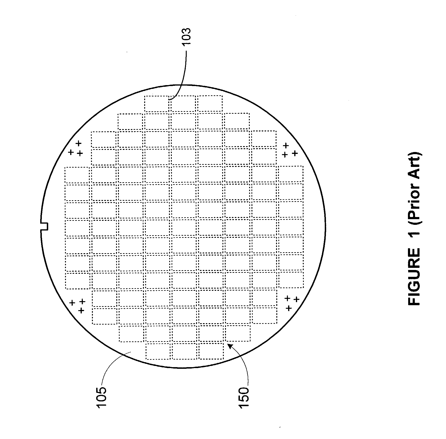
Method and apparatus for selecting sites for sampling
PatentInactiveUS7330800B1
Innovation
- A method involving dynamic site selection based on sampling rules with associated penalties, where a subset of sites on a semiconductor wafer is chosen for metrology, optimizing the sampling plan to improve data collection efficiency and within-wafer uniformity visibility.


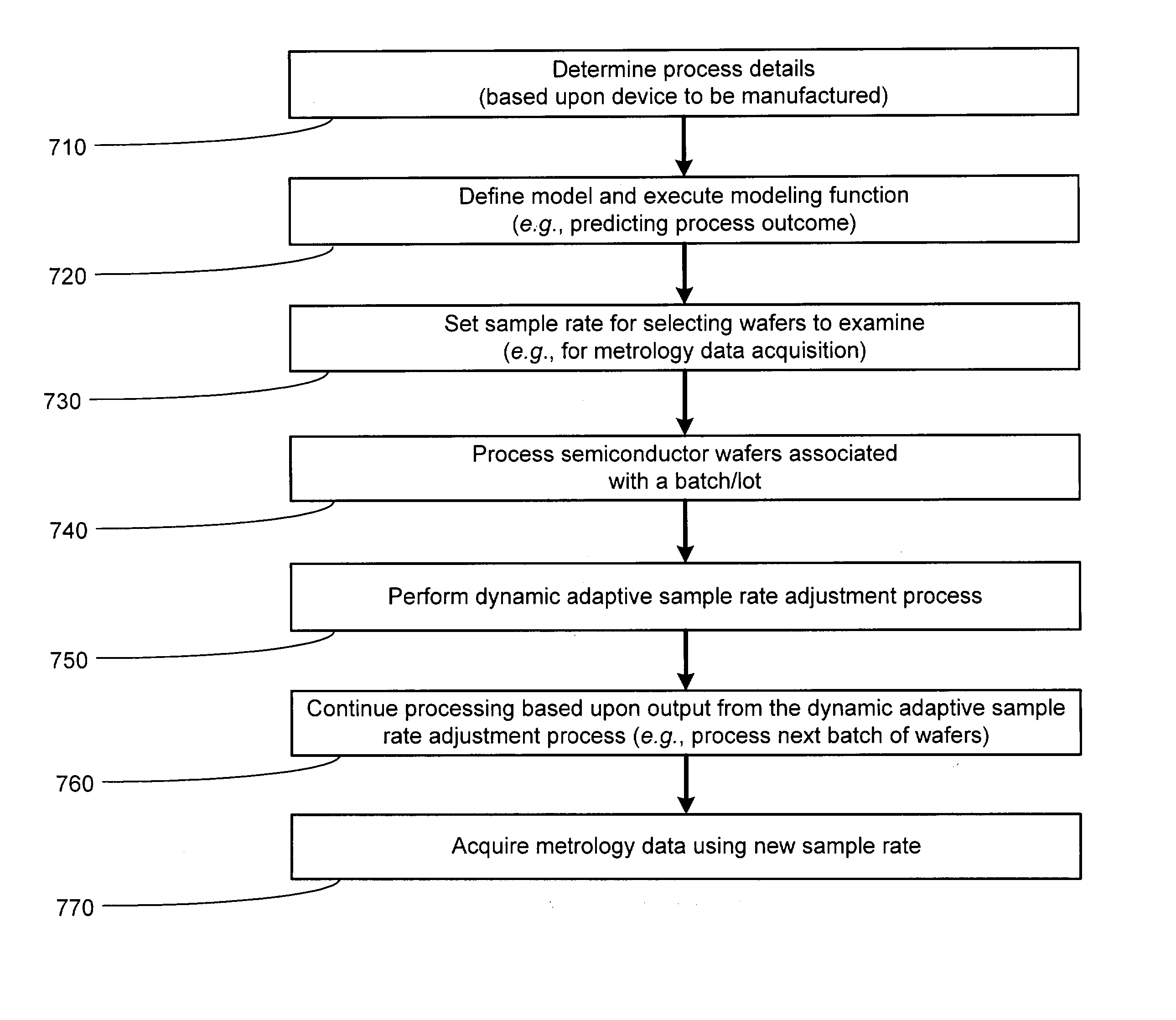
Dynamic adaptive sampling rate for model prediction
PatentInactiveUS20040121495A1
Innovation
- A dynamic sampling rate adjustment method that compares predicted and actual process outcomes to adaptively modify the sampling rate, ensuring sufficient metrology data acquisition based on the uncertainty of the process model, thereby enhancing the accuracy of process control.

Quality Standards for Semiconductor Metrology Systems
Quality standards for semiconductor metrology systems represent a critical framework that governs the precision, accuracy, and reliability requirements for wafer measurement equipment. These standards establish the foundational benchmarks that metrology systems must meet to ensure consistent and trustworthy measurements across semiconductor manufacturing processes.
The International Technology Roadmap for Semiconductors (ITRS) and its successor, the International Roadmap for Devices and Systems (IRDS), define stringent precision requirements for critical dimension measurements, overlay accuracy, and film thickness uniformity. These roadmaps specify that measurement uncertainties must be maintained within 10-15% of the feature size being measured, with some critical applications requiring even tighter tolerances of 5% or less.
SEMI standards, particularly SEMI E10 for specification and verification of measurement equipment, provide comprehensive guidelines for metrology system qualification. These standards mandate specific protocols for measurement repeatability, reproducibility, and long-term stability assessments. The standards require that systems demonstrate measurement precision better than one-third of the process tolerance, ensuring adequate sensitivity for process control applications.
ISO 5725 series standards complement semiconductor-specific requirements by establishing statistical methods for accuracy and precision evaluation. These standards define procedures for interlaboratory studies and measurement uncertainty calculations, which are essential for validating metrology system performance across different manufacturing sites and equipment configurations.
Quality standards also encompass environmental control requirements, specifying acceptable ranges for temperature stability, vibration isolation, and electromagnetic interference. These environmental specifications directly impact sampling error minimization by ensuring consistent measurement conditions. Temperature variations must typically be controlled within ±0.1°C, while vibration levels must remain below specified thresholds to prevent measurement artifacts.
Calibration and traceability standards require regular verification against certified reference materials and participation in round-robin measurement programs. These requirements ensure that metrology systems maintain their specified performance over time and provide measurements that are traceable to international standards, thereby minimizing systematic sampling errors across the semiconductor industry.
Cost-Benefit Analysis of Advanced Sampling Methods
The economic evaluation of advanced sampling methods in wafer metrology systems requires a comprehensive assessment of implementation costs versus operational benefits. Traditional sampling approaches, while cost-effective initially, often result in higher long-term expenses due to increased defect escape rates and yield losses. Advanced sampling techniques, including adaptive sampling algorithms and machine learning-enhanced pattern recognition, demand substantial upfront investments in software development, hardware upgrades, and personnel training.
Initial capital expenditures for implementing advanced sampling systems typically range from $500,000 to $2 million per fabrication facility, depending on the complexity of existing infrastructure and required integration levels. These costs encompass specialized metrology equipment, computational resources for real-time data processing, and software licensing fees for proprietary algorithms. Additionally, workforce development expenses account for approximately 15-20% of total implementation costs, as operators require extensive training on new sampling protocols and data interpretation methodologies.
The operational benefits of advanced sampling methods manifest through multiple channels, primarily yield improvement and defect detection efficiency. Enhanced sampling strategies can reduce sampling errors by 40-60% compared to conventional fixed-pattern approaches, translating to yield improvements of 2-5% in mature semiconductor processes. For a typical 300mm wafer fabrication facility producing 40,000 wafers monthly, this yield enhancement represents potential revenue increases of $8-15 million annually, assuming average selling prices of $1,000-2,000 per wafer.
Maintenance and operational cost reductions constitute another significant benefit category. Advanced sampling methods optimize measurement frequency and location selection, reducing unnecessary metrology operations by 25-35%. This efficiency gain decreases equipment wear, extends calibration intervals, and reduces consumable usage, resulting in annual savings of $200,000-500,000 per facility.
The return on investment timeline for advanced sampling implementations typically spans 18-36 months, with faster payback periods observed in high-volume manufacturing environments. Risk mitigation benefits, while challenging to quantify precisely, provide additional value through reduced customer returns, warranty claims, and reputation protection. Long-term competitive advantages include improved process control capabilities and enhanced ability to support next-generation technology nodes with tighter specification requirements.
Unlock deeper insights with PatSnap Eureka Quick Research — get a full tech report to explore trends and direct your research. Try now!
Generate Your Research Report Instantly with AI Agent
Supercharge your innovation with PatSnap Eureka AI Agent Platform!