

Wafer Metrology for MEMS Devices: Precise Surface Analysis Methods
MAY 19, 20269 MIN READ
Generate Your Research Report Instantly with AI Agent
PatSnap Eureka helps you evaluate technical feasibility & market potential.
MEMS Wafer Metrology Background and Objectives
MEMS (Micro-Electro-Mechanical Systems) technology has emerged as a cornerstone of modern semiconductor manufacturing, enabling the integration of mechanical elements, sensors, actuators, and electronics on a common silicon substrate. The evolution of MEMS devices from simple pressure sensors in the 1980s to today's sophisticated inertial measurement units, microphones, and optical components has been driven by continuous advancements in fabrication techniques and metrology capabilities.
The historical development of MEMS wafer metrology can be traced through several key phases. Initially, conventional semiconductor metrology tools were adapted for MEMS applications, but the unique three-dimensional structures and diverse material compositions of MEMS devices quickly revealed the limitations of traditional measurement approaches. The introduction of specialized surface profiling techniques in the 1990s marked a significant milestone, followed by the development of non-contact optical methods and advanced interferometric systems in the 2000s.
Current technological trends indicate a shift toward higher precision, faster throughput, and multi-parameter measurement capabilities. The industry is witnessing increased adoption of white light interferometry, atomic force microscopy, and advanced optical profilometry techniques. These methods enable comprehensive characterization of critical MEMS parameters including surface roughness, step heights, film thickness, and structural dimensions with nanometer-level precision.
The primary objective of modern MEMS wafer metrology is to establish robust measurement methodologies that can accurately characterize the complex geometries and material properties inherent in MEMS devices. This includes developing techniques capable of measuring high aspect ratio structures, curved surfaces, and multi-layer thin films while maintaining the speed and reliability required for high-volume manufacturing environments.
Key technical goals encompass achieving sub-nanometer measurement precision for critical dimensions, implementing real-time process monitoring capabilities, and establishing comprehensive quality control frameworks. The integration of artificial intelligence and machine learning algorithms into metrology systems represents an emerging objective, aimed at enhancing defect detection capabilities and predictive maintenance protocols.
Furthermore, the industry seeks to develop standardized measurement protocols that can accommodate the diverse range of MEMS device architectures, from simple cantilevers to complex multi-physics systems, ensuring consistent quality metrics across different manufacturing facilities and product lines.
Market Demand for Precise MEMS Surface Analysis
The global MEMS market has experienced unprecedented growth, driven by the proliferation of consumer electronics, automotive applications, and industrial automation systems. This expansion has created substantial demand for advanced wafer metrology solutions capable of delivering precise surface analysis for MEMS devices. The miniaturization trend in electronics continues to push the boundaries of manufacturing precision, requiring increasingly sophisticated measurement and characterization techniques.
Consumer electronics represent the largest market segment driving demand for MEMS surface analysis capabilities. Smartphones, tablets, and wearable devices incorporate multiple MEMS components including accelerometers, gyroscopes, microphones, and pressure sensors. Each device requires stringent quality control measures to ensure optimal performance and reliability. The surface characteristics of these components directly impact their functionality, making precise metrology essential for manufacturers to maintain competitive advantages.
The automotive industry has emerged as a critical growth driver for MEMS metrology demand. Modern vehicles integrate numerous MEMS-based sensors for safety systems, navigation, and autonomous driving capabilities. Automotive applications demand exceptional reliability and longevity, necessitating comprehensive surface analysis during manufacturing processes. The transition toward electric vehicles and advanced driver assistance systems further amplifies the need for high-precision MEMS components.
Industrial Internet of Things applications continue expanding the addressable market for MEMS devices. Smart manufacturing, environmental monitoring, and process control systems rely heavily on MEMS sensors for data collection and system optimization. These applications often operate in harsh environments, requiring robust surface characteristics that can only be verified through advanced metrology techniques.
The semiconductor industry's ongoing evolution toward smaller node sizes and three-dimensional structures has intensified the complexity of MEMS manufacturing processes. Traditional metrology approaches often prove inadequate for characterizing the intricate surface features and material properties required for next-generation devices. This technological gap has created substantial market opportunities for innovative surface analysis solutions.
Emerging applications in healthcare and biotechnology sectors present additional growth vectors for MEMS metrology demand. Medical devices, diagnostic equipment, and implantable sensors require exceptional precision and biocompatibility. Surface analysis becomes critical for ensuring device safety and efficacy in biological environments.
The market demand extends beyond traditional dimensional measurements to encompass comprehensive material characterization, stress analysis, and defect detection capabilities. Manufacturers increasingly require integrated metrology solutions that can provide real-time feedback for process optimization and yield enhancement.
Current MEMS Metrology Challenges and Limitations
MEMS wafer metrology faces significant challenges in achieving the precision required for modern microelectromechanical systems manufacturing. Traditional optical measurement techniques struggle with the complex three-dimensional structures characteristic of MEMS devices, where features often include deep trenches, high aspect ratio structures, and multi-level topographies that create shadowing effects and measurement blind spots.
Surface roughness characterization presents particular difficulties due to the diverse materials used in MEMS fabrication. Silicon, silicon dioxide, polysilicon, and various metal layers each exhibit different optical and mechanical properties, requiring specialized measurement approaches. Conventional stylus profilometry, while accurate for simple surfaces, cannot adequately navigate the intricate geometries of MEMS structures without risk of damage or measurement artifacts.
The dimensional scaling of MEMS devices has outpaced the resolution capabilities of many established metrology tools. Critical dimensions now routinely fall below 100 nanometers, demanding measurement precision that approaches the fundamental limits of optical wavelengths. This scaling challenge is compounded by the need to measure features with extreme aspect ratios, where depths can exceed widths by factors of 50:1 or greater.
Process-induced variations create additional metrology complications. MEMS manufacturing involves numerous etching, deposition, and thermal processing steps that can introduce stress-related deformations, making it difficult to distinguish between intentional design features and process artifacts. The measurement of suspended structures, such as cantilevers and membranes, requires non-contact methods that can assess mechanical properties alongside dimensional characteristics.
Throughput limitations represent a critical bottleneck in production environments. High-resolution measurement techniques often require extended acquisition times that are incompatible with manufacturing cycle requirements. The trade-off between measurement speed and precision becomes particularly acute when attempting to implement comprehensive wafer-level inspection protocols.
Temperature and environmental sensitivity further complicate MEMS metrology. Many measurement techniques are susceptible to thermal drift and vibration, while MEMS devices themselves may exhibit temperature-dependent dimensional changes that must be distinguished from measurement errors. The need for controlled measurement environments adds complexity and cost to metrology implementations.
Data interpretation challenges arise from the multi-parameter nature of MEMS characterization, where surface topography, material properties, and mechanical behavior must be simultaneously evaluated and correlated to predict device performance and reliability.
Existing MEMS Surface Characterization Solutions
01 Advanced optical measurement systems for wafer surface characterization
Sophisticated optical measurement technologies are employed to analyze wafer surface properties with high precision. These systems utilize various optical techniques including interferometry, ellipsometry, and spectroscopic methods to detect surface variations, thickness measurements, and material properties. The optical approaches enable non-destructive analysis while maintaining nanometer-level accuracy for critical dimension measurements and surface topography assessment.- Advanced optical measurement systems for wafer surface characterization: Sophisticated optical measurement technologies are employed to analyze wafer surface properties with high precision. These systems utilize various optical techniques including interferometry, ellipsometry, and spectroscopic methods to detect surface defects, measure thickness variations, and characterize material properties. The optical approaches enable non-destructive analysis while maintaining nanometer-level accuracy for critical dimension measurements and surface roughness evaluation.
- Scanning probe microscopy techniques for surface topography analysis: Scanning probe microscopy methods provide atomic-scale resolution for wafer surface analysis. These techniques include atomic force microscopy and scanning tunneling microscopy approaches that can map surface topography, measure local electrical properties, and detect nanoscale defects. The high-resolution capabilities enable precise characterization of surface features and contamination at the molecular level, which is critical for advanced semiconductor manufacturing processes.
- Multi-sensor integration and data fusion for comprehensive metrology: Integration of multiple measurement sensors and data fusion algorithms enhance the overall precision and reliability of wafer surface analysis. These systems combine different measurement modalities to provide comprehensive surface characterization, reduce measurement uncertainties, and improve defect detection capabilities. Advanced signal processing and machine learning algorithms are employed to correlate data from various sensors and extract meaningful surface parameters.
- Real-time process monitoring and feedback control systems: Real-time monitoring systems enable continuous assessment of wafer surface quality during manufacturing processes. These systems provide immediate feedback for process control and adjustment, helping to maintain consistent surface properties and reduce defect formation. The monitoring approaches include in-situ measurement capabilities that can detect surface changes during processing without interrupting the manufacturing workflow.
- Statistical analysis and pattern recognition for defect classification: Advanced statistical methods and pattern recognition algorithms are applied to analyze measurement data and classify surface defects. These approaches enable automated identification of different types of surface anomalies, trend analysis for process optimization, and predictive maintenance capabilities. Machine learning techniques help improve the accuracy of defect detection and reduce false positive rates in surface quality assessment.
02 Scanning probe microscopy techniques for surface analysis
Scanning probe microscopy methods provide atomic-level resolution for wafer surface analysis and metrology applications. These techniques include atomic force microscopy and scanning tunneling microscopy approaches that can measure surface roughness, defect detection, and three-dimensional topographical mapping. The scanning probe methods offer exceptional precision for characterizing nanoscale features and surface irregularities critical for semiconductor manufacturing quality control.Expand Specific Solutions03 Multi-sensor integration and data fusion for enhanced precision
Integration of multiple measurement sensors and data fusion algorithms significantly improves the accuracy and reliability of wafer surface analysis. These systems combine different measurement modalities to cross-validate results and reduce measurement uncertainties. The multi-sensor approach enables comprehensive surface characterization by leveraging the strengths of various measurement techniques while compensating for individual sensor limitations.Expand Specific Solutions04 Real-time monitoring and feedback control systems
Real-time monitoring capabilities enable continuous surface analysis during wafer processing with immediate feedback for process control. These systems provide instantaneous measurement data that can be used to adjust manufacturing parameters and maintain consistent surface quality. The real-time approach minimizes defects and improves yield by detecting surface anomalies early in the manufacturing process.Expand Specific Solutions05 Machine learning and AI-enhanced surface defect detection
Artificial intelligence and machine learning algorithms are implemented to enhance surface defect detection and classification accuracy. These intelligent systems can identify subtle surface anomalies that might be missed by traditional analysis methods and provide predictive insights for process optimization. The AI-enhanced approaches improve measurement precision through pattern recognition and automated decision-making capabilities.Expand Specific Solutions
Key Players in MEMS Metrology Equipment Industry
The wafer metrology for MEMS devices market represents a mature yet rapidly evolving sector driven by increasing demand for precision surface analysis in semiconductor manufacturing. The industry is experiencing significant growth, with market expansion fueled by automotive, IoT, and consumer electronics applications requiring enhanced MEMS performance. Technology maturity varies across segments, with established players like Tokyo Electron Ltd., Nikon Corp., and Zygo Corp. leading advanced optical metrology solutions, while companies such as FemtoMetrix Inc. and Unity Semiconductor SAS drive innovation in specialized inspection technologies. Manufacturing giants including Semiconductor Manufacturing International Corp., Micron Technology Inc., and GlobalWafers Co. Ltd. represent the demand side, implementing these metrology solutions for quality assurance. The competitive landscape features a mix of established equipment manufacturers, emerging technology specialists, and research institutions like Southeast University and Peking University contributing to technological advancement, indicating a healthy ecosystem supporting continued innovation in MEMS surface analysis methodologies.
Hitachi High-Tech America, Inc.
Technical Solution: Hitachi High-Tech develops advanced critical dimension scanning electron microscopy (CD-SEM) systems specifically designed for MEMS wafer metrology. Their technology incorporates ultra-high resolution imaging capabilities with sub-nanometer precision for surface topography analysis. The company's metrology solutions feature automated defect detection algorithms and real-time process monitoring systems that can identify surface irregularities, dimensional variations, and structural defects in MEMS devices. Their systems utilize advanced electron beam technology combined with sophisticated image processing software to provide comprehensive surface characterization including roughness measurements, step height analysis, and critical dimension verification for complex MEMS structures.
Strengths: Industry-leading electron microscopy technology with exceptional resolution and automated analysis capabilities. Weaknesses: High equipment costs and complex operation requirements may limit accessibility for smaller manufacturers.
FemtoMetrix, Inc.
Technical Solution: FemtoMetrix specializes in innovative pump-probe metrology technology for advanced MEMS wafer surface analysis. Their proprietary technique uses ultrafast laser pulses to generate and detect acoustic waves within materials, enabling non-destructive measurement of subsurface properties and mechanical characteristics of MEMS structures. The technology provides unique capabilities for measuring elastic modulus, adhesion strength, and interfacial properties that are critical for MEMS device reliability. FemtoMetrix systems can detect delamination, void formation, and other subsurface defects that traditional surface metrology techniques cannot identify. Their solutions offer high spatial resolution mapping capabilities and can analyze complex multilayer MEMS structures with varying material properties, providing comprehensive characterization data for process development and quality control applications.
Strengths: Unique subsurface analysis capabilities with non-destructive testing and high sensitivity to mechanical properties. Weaknesses: Specialized technology with limited market penetration and higher complexity compared to conventional surface metrology methods.
Core Innovations in Precision MEMS Metrology
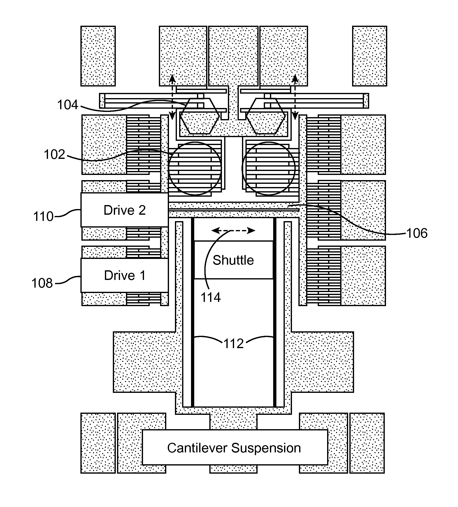
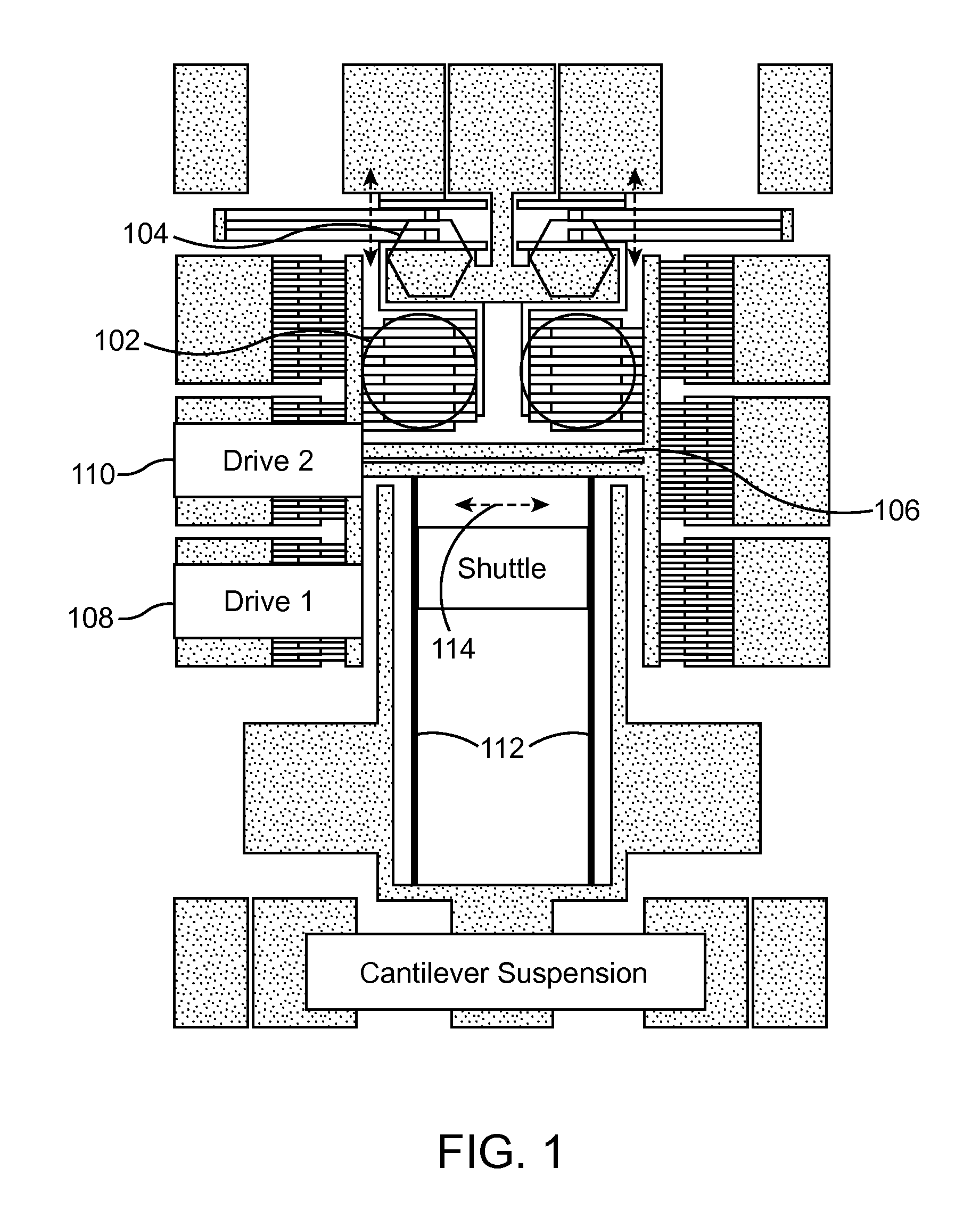
Integrated MEMS metrology device using complementary measuring combs
PatentInactiveUS8079246B2
Innovation
- A MEMS metrology device utilizing comb drives with a translating shuttle and measuring combs to measure displacement and electrical capacitance, allowing for in-situ monitoring of material, process, and dynamic properties, which is compact, inexpensive, and suitable for on-chip integration.
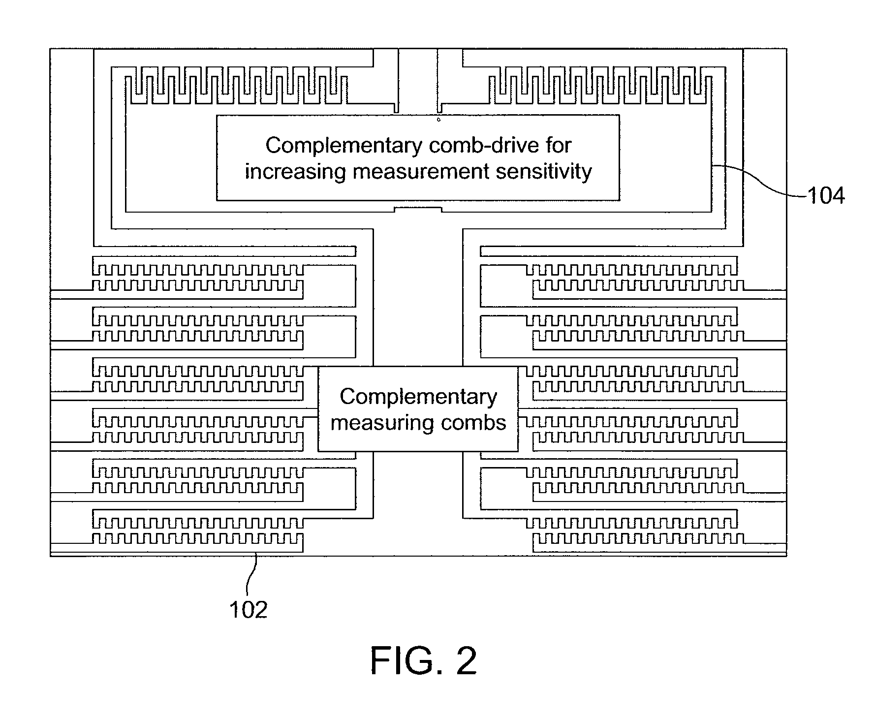

Integrated MEMS metrology device using complementary measuring combs
PatentWO2007124357A2
Innovation
- An integrated MEMS metrology device using complementary measuring combs with cantilever suspensions and comb drives for in-situ monitoring, allowing for nondestructive, accurate measurement of material, process, and dynamic properties, which can be deployed in arrays and integrated on-chip.

Semiconductor Manufacturing Standards and Compliance
The semiconductor manufacturing industry operates under a comprehensive framework of standards and compliance requirements that directly impact wafer metrology for MEMS devices. International standards organizations such as SEMI, ISO, and ASTM have established critical guidelines governing surface analysis methodologies, measurement accuracy, and quality control protocols. These standards ensure consistency across global manufacturing facilities and enable reliable comparison of metrology results between different equipment vendors and measurement techniques.
SEMI standards play a particularly crucial role in defining specifications for wafer handling, contamination control, and measurement procedures. Standards such as SEMI M1 for test wafers, SEMI M20 for particle counting, and SEMI M58 for surface roughness measurements provide the foundation for precise MEMS device characterization. Compliance with these standards is mandatory for semiconductor manufacturers seeking to maintain product quality and achieve certification from major customers in automotive, aerospace, and consumer electronics sectors.
Regulatory compliance extends beyond technical specifications to encompass environmental, health, and safety requirements. The implementation of precise surface analysis methods must adhere to regulations governing chemical usage, waste disposal, and worker safety protocols. This is particularly relevant for MEMS metrology processes that involve advanced analytical techniques such as X-ray photoelectron spectroscopy, atomic force microscopy, and scanning electron microscopy, which may utilize hazardous materials or generate potentially harmful emissions.
Quality management systems such as ISO 9001 and automotive-specific standards like IATF 16949 mandate rigorous documentation and traceability requirements for all metrology processes. These standards require comprehensive calibration procedures, measurement uncertainty analysis, and statistical process control implementation. For MEMS wafer metrology, this translates to detailed protocols for equipment qualification, measurement repeatability validation, and long-term stability monitoring of surface analysis instruments.
The emergence of Industry 4.0 and smart manufacturing concepts has introduced additional compliance considerations related to data security, cybersecurity, and digital traceability. Modern wafer metrology systems must comply with standards governing data integrity, secure communication protocols, and automated reporting capabilities while maintaining the precision required for advanced MEMS device manufacturing.
Quality Control Framework for MEMS Production
A comprehensive quality control framework for MEMS production represents a systematic approach to ensuring consistent device performance and reliability throughout the manufacturing process. This framework integrates multiple inspection stages, from incoming wafer qualification to final device testing, establishing critical control points that prevent defective products from advancing through the production pipeline.
The foundation of effective MEMS quality control lies in establishing standardized measurement protocols that address the unique characteristics of microelectromechanical systems. Unlike traditional semiconductor devices, MEMS components require specialized inspection techniques that can accurately assess three-dimensional structures, mechanical properties, and surface integrity at microscale dimensions. These protocols must accommodate the diverse range of MEMS device architectures while maintaining measurement repeatability and accuracy.
Statistical process control forms the backbone of modern MEMS quality frameworks, enabling real-time monitoring of critical parameters and early detection of process variations. Implementation of control charts, capability studies, and trend analysis allows production teams to identify potential issues before they impact device yield or performance. The framework incorporates both parametric and functional testing methodologies to ensure comprehensive coverage of device specifications.
Traceability systems within the quality framework enable complete documentation of each device's manufacturing history, from raw material sourcing through final packaging. This comprehensive record-keeping facilitates rapid root cause analysis when quality issues arise and supports continuous improvement initiatives. Integration with manufacturing execution systems ensures seamless data flow and automated decision-making capabilities.
Risk-based inspection strategies optimize resource allocation by focusing intensive quality control efforts on high-risk process steps and critical device features. This approach balances thorough quality assurance with production efficiency, utilizing sampling plans and inspection frequencies tailored to specific process capabilities and historical performance data.
The framework incorporates feedback mechanisms that translate quality data into actionable process improvements, creating a closed-loop system for continuous enhancement of manufacturing capabilities. Regular calibration schedules, measurement system analysis, and inter-laboratory comparisons ensure the integrity and reliability of quality control measurements throughout the production environment.
Unlock deeper insights with PatSnap Eureka Quick Research — get a full tech report to explore trends and direct your research. Try now!
Generate Your Research Report Instantly with AI Agent
Supercharge your innovation with PatSnap Eureka AI Agent Platform!