

How to Use AI Algorithms in VLSI Layout Optimization
MAR 7, 20269 MIN READ
Generate Your Research Report Instantly with AI Agent
PatSnap Eureka helps you evaluate technical feasibility & market potential.
AI-Driven VLSI Layout Background and Objectives
The integration of artificial intelligence algorithms into Very Large Scale Integration (VLSI) layout optimization represents a paradigm shift in semiconductor design methodology. Traditional VLSI layout design has long relied on rule-based algorithms and heuristic approaches, which, while effective for smaller designs, struggle to cope with the exponential complexity growth in modern integrated circuits. As semiconductor technology nodes continue to shrink and transistor counts reach billions per chip, conventional optimization techniques face significant scalability and efficiency limitations.
The evolution of VLSI layout optimization has progressed through several distinct phases. Early approaches in the 1980s focused on geometric algorithms and graph-based methods for placement and routing problems. The 1990s introduced simulated annealing and genetic algorithms, marking the first systematic application of optimization techniques. The 2000s saw the emergence of analytical placement methods and global routing algorithms that could handle million-gate designs. However, these traditional methods increasingly struggle with contemporary challenges such as multi-objective optimization, design rule complexity, and manufacturing variability.
Modern semiconductor designs present unprecedented complexity challenges that demand innovative solutions. Current designs must simultaneously optimize for power consumption, performance, area utilization, thermal management, and manufacturability while satisfying thousands of design rules. The interdependencies between these objectives create a multi-dimensional optimization space that traditional algorithms cannot efficiently navigate. Additionally, the increasing importance of parasitic effects, signal integrity, and electromigration reliability further complicates the optimization landscape.
The primary objective of incorporating AI algorithms into VLSI layout optimization is to develop intelligent systems capable of learning from design patterns, predicting optimization outcomes, and making informed decisions in complex design spaces. Machine learning techniques, particularly deep learning and reinforcement learning, offer the potential to automatically discover optimal design strategies that surpass human expertise and traditional algorithmic approaches.
Key technical objectives include developing AI models that can predict placement quality, optimize routing congestion, minimize wirelength while maintaining timing constraints, and adapt to different technology nodes and design styles. The ultimate goal is to create autonomous design systems that can generate high-quality layouts with minimal human intervention, significantly reducing design time while improving overall chip performance and manufacturability.
Market Demand for AI-Enhanced VLSI Design Tools
The semiconductor industry is experiencing unprecedented demand for advanced VLSI design tools enhanced with artificial intelligence capabilities. This surge stems from the increasing complexity of modern chip designs, where traditional manual layout optimization methods have reached their practical limitations. As transistor densities continue to scale according to Moore's Law, designers face exponentially growing design spaces that require intelligent automation to navigate effectively.
Market drivers for AI-enhanced VLSI design tools are multifaceted and compelling. The proliferation of specialized processors for artificial intelligence, machine learning, and edge computing applications has created a need for highly optimized layouts that can maximize performance while minimizing power consumption and area. These requirements cannot be adequately addressed through conventional Electronic Design Automation tools alone, necessitating the integration of sophisticated AI algorithms.
The automotive industry's transition toward autonomous vehicles and electric powertrains represents a significant growth catalyst. Advanced driver assistance systems and autonomous driving platforms require custom silicon solutions with stringent reliability, performance, and power efficiency requirements. AI-enhanced layout optimization tools enable designers to achieve these demanding specifications while reducing development time and costs.
Data center and cloud computing infrastructure demands continue to escalate, driving requirements for specialized processors optimized for specific workloads. Hyperscale data center operators seek custom silicon solutions that can deliver superior performance per watt compared to general-purpose processors. AI-powered layout optimization tools enable the creation of these highly specialized designs by automatically exploring vast solution spaces and identifying optimal configurations.
The Internet of Things ecosystem presents another substantial market opportunity. IoT devices require ultra-low-power designs with minimal silicon area to achieve cost-effective manufacturing at scale. AI algorithms can optimize layouts to achieve these challenging constraints while maintaining functional requirements, making previously impractical designs commercially viable.
Mobile device manufacturers face continuous pressure to integrate more functionality into smaller form factors while extending battery life. AI-enhanced VLSI design tools enable the creation of highly integrated system-on-chip solutions that meet these demanding requirements through intelligent placement, routing, and power optimization strategies.
Enterprise adoption of AI-enhanced design tools is accelerating as organizations recognize the competitive advantages of reduced design cycles, improved design quality, and enhanced engineering productivity. The market demand reflects a fundamental shift toward intelligent automation in semiconductor design workflows.
Current State of AI in VLSI Layout Optimization
The integration of artificial intelligence algorithms into VLSI layout optimization has reached a significant maturity level, with multiple AI paradigms demonstrating substantial improvements over traditional electronic design automation tools. Current implementations primarily leverage machine learning techniques including reinforcement learning, deep neural networks, and genetic algorithms to address the complex multi-objective optimization challenges inherent in modern semiconductor design.
Reinforcement learning has emerged as the dominant approach, with Google's breakthrough work on chip floorplanning using deep Q-networks setting new industry benchmarks. Their system achieved 6% improvement in power consumption and 11% reduction in wire length compared to human experts. This success has catalyzed widespread adoption across major EDA companies, with Synopsys, Cadence, and Mentor Graphics incorporating RL-based optimization engines into their commercial tools.
Deep learning architectures, particularly convolutional neural networks and graph neural networks, are extensively deployed for placement prediction and routing optimization. These models excel at pattern recognition in layout geometries and can predict optimal component positioning with remarkable accuracy. Current implementations achieve convergence times that are 10-100 times faster than traditional simulated annealing approaches while maintaining comparable or superior solution quality.
Genetic algorithms and evolutionary computation methods continue to play crucial roles in handling discrete optimization problems within layout design. Modern hybrid approaches combine evolutionary strategies with gradient-based optimization, enabling efficient exploration of vast design spaces while avoiding local optima. These techniques are particularly effective for analog circuit layout optimization where design constraints are highly nonlinear.
Graph-based AI algorithms have gained prominence for addressing interconnect optimization challenges. Graph neural networks can effectively model the complex relationships between circuit components and predict optimal routing paths. Recent advances in graph attention mechanisms allow these systems to dynamically focus on critical design regions, improving both performance and interpretability.
The current technological landscape shows strong momentum toward multi-agent reinforcement learning systems that can simultaneously optimize placement, routing, and timing closure. These integrated approaches represent a significant departure from traditional sequential optimization workflows, offering the potential for global optimization across all design phases.
Despite these advances, current AI-driven VLSI optimization tools still face limitations in handling extremely large-scale designs exceeding millions of components, and integration challenges with existing design flows remain a significant barrier to widespread industrial adoption.
Existing AI Solutions for Layout Optimization
01 Machine learning-based layout optimization algorithms
AI algorithms utilize machine learning techniques to optimize layout designs by analyzing patterns and learning from existing data. These algorithms can automatically adjust and improve layout configurations through iterative training processes, enabling adaptive optimization based on various constraints and objectives. The machine learning approach allows for intelligent decision-making in complex layout scenarios.- Machine learning-based layout optimization algorithms: Advanced machine learning algorithms are employed to optimize layout designs by analyzing patterns and predicting optimal configurations. These algorithms can process large datasets to identify efficient spatial arrangements and improve design quality. Neural networks and deep learning models are trained to recognize layout constraints and generate optimized solutions automatically. The algorithms can adapt to different design requirements and continuously improve through iterative learning processes.
- Reinforcement learning for adaptive layout generation: Reinforcement learning techniques are utilized to create adaptive layout systems that learn from feedback and improve over time. These methods enable the system to explore different layout configurations and select optimal arrangements based on reward mechanisms. The approach allows for dynamic adjustment of layouts in response to changing constraints and requirements. This technology is particularly effective for complex design spaces where traditional optimization methods may be insufficient.
- Genetic algorithms and evolutionary computation for layout design: Genetic algorithms and evolutionary computation methods are applied to solve layout optimization problems through simulated evolution processes. These algorithms use selection, crossover, and mutation operations to generate and refine layout solutions across multiple generations. The approach is effective for handling multi-objective optimization problems where multiple design criteria must be balanced. Population-based search strategies enable exploration of diverse solution spaces to find globally optimal or near-optimal layouts.
- Graph neural networks for spatial relationship optimization: Graph neural networks are employed to model and optimize spatial relationships in layout designs by representing elements as nodes and their relationships as edges. This approach enables the algorithm to understand complex dependencies and constraints between layout components. The network can learn hierarchical structures and propagate information across the layout to achieve global optimization. This method is particularly suitable for layouts with intricate connectivity requirements and spatial constraints.
- Hybrid optimization combining multiple AI techniques: Hybrid optimization approaches integrate multiple artificial intelligence techniques to leverage their complementary strengths for layout optimization. These systems may combine heuristic methods with machine learning models to balance exploration and exploitation in the search process. The integration of different algorithms allows for handling various aspects of layout optimization simultaneously, such as area minimization, routing efficiency, and constraint satisfaction. Multi-stage optimization pipelines can progressively refine layouts from initial rough designs to detailed final configurations.
02 Neural network architectures for spatial arrangement
Deep learning and neural network models are employed to solve spatial arrangement problems in layout optimization. These architectures can process multi-dimensional layout data and generate optimized configurations by learning complex spatial relationships. The neural network approach enables handling of non-linear optimization problems and can adapt to different layout requirements through training.Expand Specific Solutions03 Reinforcement learning for iterative layout improvement
Reinforcement learning algorithms are applied to continuously improve layout designs through reward-based feedback mechanisms. These algorithms explore different layout configurations and learn optimal strategies by receiving feedback on design quality. The iterative nature allows for progressive refinement of layouts while balancing multiple optimization objectives.Expand Specific Solutions04 Genetic algorithms and evolutionary computation methods
Evolutionary algorithms and genetic programming techniques are utilized to search the solution space for optimal layout configurations. These methods simulate natural selection processes to evolve better layout designs over generations. The approach is particularly effective for handling multi-objective optimization problems with complex constraints.Expand Specific Solutions05 Hybrid AI approaches combining multiple optimization techniques
Integrated systems combine multiple AI methodologies such as heuristic algorithms, constraint satisfaction, and optimization frameworks to achieve superior layout results. These hybrid approaches leverage the strengths of different algorithms to handle various aspects of layout optimization simultaneously. The combination enables more robust and efficient solutions for complex layout problems.Expand Specific Solutions
Key Players in AI-Powered VLSI Design Industry
The AI-driven VLSI layout optimization field represents a rapidly evolving sector within the semiconductor industry, currently in its growth phase as traditional EDA approaches integrate machine learning capabilities. The market demonstrates significant expansion potential, driven by increasing chip complexity and demand for automated design solutions. Technology maturity varies considerably across market participants, with established EDA leaders like Synopsys and Siemens Industry Software offering mature AI-enhanced tools, while semiconductor giants including NVIDIA, Samsung Electronics, and IBM drive innovation through proprietary optimization algorithms. Foundries such as GLOBALFOUNDRIES and SMIC are implementing AI-driven manufacturing optimization, while emerging players like Groq focus on specialized AI acceleration hardware. Academic institutions including Tianjin University and University of California contribute fundamental research, creating a diverse ecosystem spanning from mature commercial solutions to cutting-edge research initiatives, positioning the field for continued technological advancement and market growth.
International Business Machines Corp.
Technical Solution: IBM applies AI algorithms in VLSI layout optimization through their AI-powered design automation framework, which combines machine learning with traditional EDA methodologies. Their approach utilizes deep reinforcement learning agents that learn optimal placement and routing strategies by interacting with the design environment and receiving feedback based on performance metrics. IBM employs graph neural networks to model circuit connectivity and predict optimal component placement, while using evolutionary algorithms for multi-objective optimization of power, performance, and area constraints. Their AI system incorporates natural language processing techniques to automatically generate design constraints from specifications, and computer vision algorithms to analyze layout patterns for design rule violations. The platform uses ensemble learning methods combining multiple AI models to improve prediction accuracy for timing closure and power estimation. IBM's AI-driven approach has demonstrated up to 15% improvement in design efficiency and 25% reduction in design cycle time compared to conventional methods.
Strengths: Strong AI research capabilities, extensive semiconductor experience, robust enterprise solutions. Weaknesses: Limited market share in EDA tools, complex integration requirements, higher implementation costs.
Synopsys, Inc.
Technical Solution: Synopsys has developed comprehensive AI-driven VLSI layout optimization solutions through their Design.ai platform, which integrates machine learning algorithms into their digital design flow. Their DSO.ai (Design Space Optimization AI) uses reinforcement learning and neural networks to automatically explore design spaces and optimize PPA (Power, Performance, Area) metrics. The platform employs deep learning models to predict routing congestion, timing violations, and power consumption during early design stages, enabling designers to make informed decisions before detailed implementation. Their AI algorithms can reduce design closure time by up to 10x while improving QoR (Quality of Results) by 20% compared to traditional methods. The system uses convolutional neural networks for layout pattern recognition and genetic algorithms for placement optimization, creating an end-to-end AI-assisted design methodology.
Strengths: Industry-leading EDA tools with proven AI integration, comprehensive design flow coverage, strong customer base. Weaknesses: High licensing costs, complexity requiring extensive training, potential vendor lock-in issues.
Core AI Innovations in VLSI Placement and Routing
Design and integration of ai-enhanced VLSI systems for accelerated machine learning processing
PatentPendingIN202441067611A
Innovation
- An AI-enhanced VLSI architecture with modular design, including AI-Optimized Processing Units, Neural Network Acceleration Core, AI-Enhanced Memory Management Unit, Interconnect Network with AI-Based Traffic Optimization, and Power Management System, which dynamically adjusts processing parameters, memory access, and power delivery to enhance performance and efficiency.

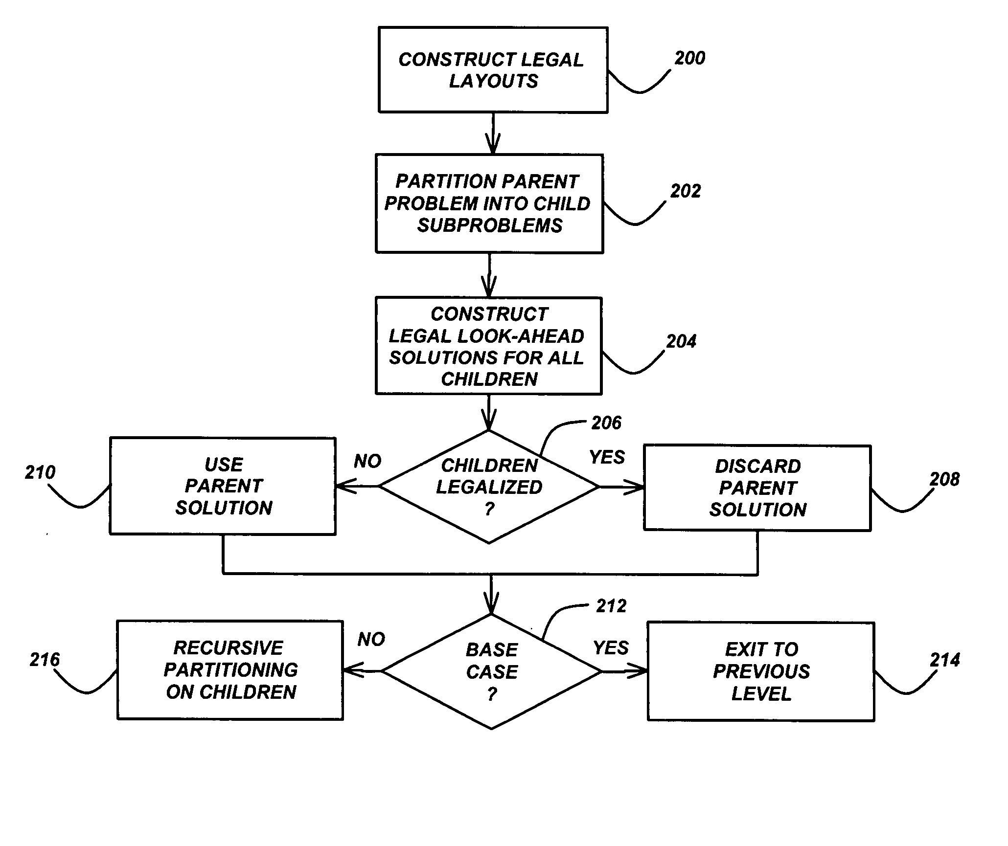
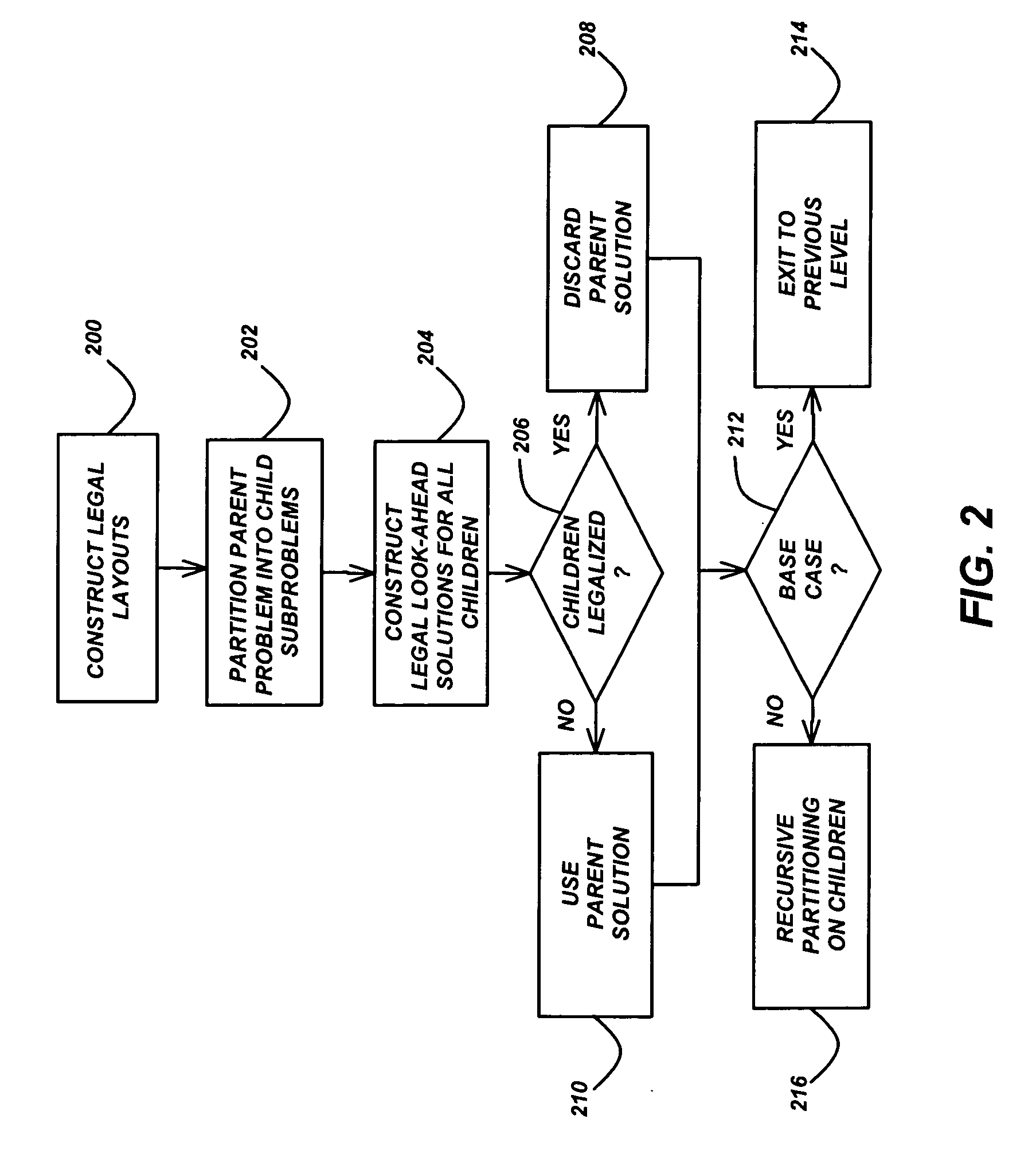
Circuit floorplanning and placement by look-ahead enabled recursive partitioning
PatentInactiveUS20060190889A1
Innovation
- The PATOMA methodology employs recursive partitioning with explicit legalization at every level of the hierarchy, using guarantor algorithms to ensure legal layouts and eliminate backtracking, thereby guaranteeing overlap-free solutions and reducing wirelength.
IP Protection in AI-Enhanced VLSI Design
The integration of artificial intelligence algorithms into VLSI layout optimization has created unprecedented challenges in intellectual property protection, fundamentally altering the traditional landscape of semiconductor design security. As AI-driven optimization tools become increasingly sophisticated, they generate novel layout configurations and design methodologies that require comprehensive IP protection strategies to safeguard proprietary innovations and competitive advantages.
AI-enhanced VLSI design environments present unique vulnerabilities that traditional IP protection mechanisms struggle to address effectively. Machine learning models used in layout optimization often incorporate proprietary training datasets, algorithmic innovations, and optimization heuristics that represent significant intellectual assets. These AI components can be reverse-engineered through model extraction attacks, where adversaries query the system to reconstruct underlying algorithms or training data, potentially exposing valuable design methodologies and optimization strategies.
The complexity of protecting AI-generated layout designs stems from the difficulty in establishing clear ownership and originality of machine-generated content. Unlike human-designed layouts, AI-optimized configurations may inadvertently incorporate patterns or structures from training datasets, raising questions about derivative works and potential infringement. This ambiguity necessitates robust documentation systems that track the provenance of AI-generated designs and establish clear chains of intellectual property ownership.
Watermarking and fingerprinting technologies have emerged as critical defense mechanisms for AI-enhanced VLSI designs. These techniques embed imperceptible signatures within layout configurations that can survive various transformations and modifications while maintaining design functionality. Advanced watermarking schemes specifically designed for AI-generated content can detect unauthorized usage or distribution of proprietary optimization algorithms and layout patterns.
Federated learning approaches offer promising solutions for collaborative VLSI optimization while preserving IP confidentiality. By enabling multiple parties to jointly train optimization models without sharing raw design data, federated systems protect proprietary layout information while benefiting from collective intelligence. However, these systems require sophisticated privacy-preserving mechanisms to prevent information leakage through model updates or gradient analysis.
The regulatory landscape surrounding AI-generated IP in semiconductor design continues evolving, with patent offices worldwide grappling with questions of inventorship and patentability for AI-assisted innovations. Organizations must develop comprehensive IP strategies that encompass both traditional design elements and AI-specific components, ensuring adequate protection across the entire technology stack while maintaining compliance with emerging legal frameworks governing artificial intelligence and automated design systems.
Computational Resource Requirements for AI Layout
The computational resource requirements for AI-driven VLSI layout optimization represent a critical bottleneck that significantly impacts the practical deployment and scalability of these advanced techniques. Modern AI algorithms, particularly deep learning models used for placement and routing optimization, demand substantial computational power that often exceeds traditional EDA tool requirements by several orders of magnitude.
Memory requirements constitute the primary constraint, with large-scale neural networks requiring tens to hundreds of gigabytes of RAM for training and inference. Graph neural networks, commonly employed for circuit representation, must maintain entire chip topologies in memory simultaneously, creating memory footprints that scale quadratically with circuit complexity. For industrial-scale designs containing millions of components, memory requirements can exceed 500GB, necessitating high-end workstations or distributed computing architectures.
Processing power demands vary significantly across different AI approaches. Reinforcement learning algorithms require extensive parallel simulation capabilities, often utilizing GPU clusters with thousands of cores for reasonable training times. Deep neural networks benefit from specialized hardware accelerators, with modern implementations achieving 10-100x speedup on TPUs compared to traditional CPUs. However, the computational intensity of training phases can extend optimization cycles from hours to weeks for complex designs.
Storage requirements present additional challenges, as AI-based optimization generates massive datasets during training and inference phases. Typical implementations require 1-10TB of storage for model checkpoints, training data, and intermediate results. The need for high-speed storage systems becomes critical when processing large design databases, as I/O bottlenecks can severely impact overall performance.
Distributed computing architectures have emerged as essential solutions for managing these resource demands. Cloud-based implementations offer scalable alternatives, though data security concerns and network latency issues remain significant barriers for proprietary designs. Hybrid approaches combining local high-memory systems with cloud-based training infrastructure represent the current industry trend for balancing performance, cost, and security requirements.
Unlock deeper insights with PatSnap Eureka Quick Research — get a full tech report to explore trends and direct your research. Try now!
Generate Your Research Report Instantly with AI Agent
Supercharge your innovation with PatSnap Eureka AI Agent Platform!