Improve VLSI Transistor Switching Speed for Quantum Computing
MAR 7, 20269 MIN READ
Generate Your Research Report Instantly with AI Agent
PatSnap Eureka helps you evaluate technical feasibility & market potential.
Quantum VLSI Transistor Background and Speed Targets
Quantum computing represents a paradigm shift in computational capability, leveraging quantum mechanical phenomena such as superposition and entanglement to process information in fundamentally new ways. Unlike classical computers that operate with binary bits, quantum computers utilize quantum bits (qubits) that can exist in multiple states simultaneously. This quantum advantage enables exponential speedup for specific computational problems, including cryptography, optimization, and molecular simulation.
The evolution of quantum computing has progressed through several distinct phases since its theoretical foundation in the 1980s. Early developments focused on establishing quantum algorithms and proof-of-concept demonstrations using trapped ions and nuclear magnetic resonance systems. The 2000s witnessed the emergence of superconducting quantum circuits and photonic quantum systems, while the 2010s marked the transition toward scalable quantum processors with increasing qubit counts and improved coherence times.
Current quantum computing architectures face significant challenges in maintaining quantum coherence while achieving rapid gate operations. Superconducting quantum processors, which dominate the current landscape, require operation at millikelvin temperatures and rely on microwave pulses for qubit manipulation. These systems typically achieve gate times in the range of 10-100 nanoseconds, but decoherence times limit the computational window to microseconds.
The integration of VLSI transistor technology into quantum computing control systems has become increasingly critical as quantum processors scale beyond hundreds of qubits. Classical control electronics must interface with quantum systems through complex signal conditioning, timing synchronization, and error correction protocols. This interface represents a bottleneck where transistor switching speeds directly impact quantum gate fidelity and overall system performance.
Speed targets for quantum VLSI transistors are driven by the stringent timing requirements of quantum error correction and real-time feedback control. Quantum error correction protocols require syndrome detection and correction within microsecond timescales to prevent error propagation. This necessitates transistor switching speeds in the sub-nanosecond range, significantly faster than conventional digital applications.
The target specifications for quantum VLSI transistors include switching times below 100 picoseconds, power consumption under 1 milliwatt per gate, and operation across temperature ranges from 4K to 300K. These requirements stem from the need to minimize latency in quantum feedback loops while maintaining low heat dissipation near quantum processors operating at ultra-low temperatures.
Market Demand for High-Speed Quantum Computing Systems
The quantum computing market is experiencing unprecedented growth driven by the critical need for exponentially faster computational capabilities across multiple industries. Financial institutions are increasingly demanding quantum systems for portfolio optimization, risk analysis, and high-frequency trading algorithms that require processing vast datasets in real-time. The pharmaceutical and biotechnology sectors represent another major demand driver, where quantum computing promises to revolutionize drug discovery through molecular simulation and protein folding calculations that are computationally intractable for classical systems.
Government and defense agencies worldwide are investing heavily in quantum computing infrastructure for cryptographic applications, secure communications, and national security purposes. The urgency to develop quantum-resistant encryption methods and quantum key distribution systems has created substantial procurement budgets specifically allocated for high-performance quantum hardware. Research institutions and universities are also contributing to market demand as they establish quantum computing centers and laboratories for fundamental research and educational purposes.
The artificial intelligence and machine learning sectors are driving significant demand for quantum computing systems capable of accelerating optimization problems, neural network training, and pattern recognition tasks. Technology companies are exploring quantum advantage in areas such as supply chain optimization, traffic management, and complex scheduling problems that require rapid switching between quantum states. The telecommunications industry is particularly interested in quantum computing applications for network optimization and quantum internet infrastructure development.
Manufacturing and materials science industries are seeking quantum computing solutions for molecular modeling, catalyst design, and advanced materials development. These applications require quantum systems with extremely fast gate operations and minimal decoherence times, directly correlating with the need for improved transistor switching speeds in the underlying control electronics.
The current market demand is characterized by a preference for quantum systems that can demonstrate clear computational advantages over classical computers in specific problem domains. Organizations are willing to invest in quantum computing infrastructure provided the systems can deliver reliable, repeatable results with sufficient quantum coherence times and gate fidelities. This market pressure is driving hardware manufacturers to focus intensively on improving every aspect of quantum system performance, including the classical control electronics that manage qubit operations.
Enterprise adoption is increasingly dependent on quantum systems that can integrate seamlessly with existing high-performance computing infrastructure while providing scalable performance improvements. The demand for hybrid quantum-classical computing architectures is particularly strong, requiring quantum processors with rapid state preparation and measurement capabilities supported by ultra-fast classical control systems.
Current VLSI Switching Limitations in Quantum Applications
Current VLSI transistor switching technologies face fundamental limitations when applied to quantum computing environments, primarily due to the extreme operational requirements and environmental constraints inherent in quantum systems. Traditional CMOS transistors, operating at room temperature with switching speeds in the gigahertz range, encounter significant performance degradation when deployed in the cryogenic conditions required for quantum processors, typically operating at temperatures below 100 millikelvin.
The primary limitation stems from carrier mobility reduction at ultra-low temperatures, where conventional silicon-based transistors experience dramatically decreased conductivity. Electron and hole mobility in silicon drops exponentially as temperature decreases, resulting in switching delays that can extend from nanoseconds to microseconds. This degradation directly impacts the timing precision required for quantum gate operations, where coherence times are measured in microseconds and require sub-nanosecond control accuracy.
Thermal noise presents another critical challenge, as quantum states are extremely sensitive to electromagnetic interference. Traditional VLSI switching generates significant electrical noise during state transitions, creating decoherence in nearby qubits. The switching transients and power supply fluctuations inherent in conventional transistor designs introduce phase errors and amplitude variations that corrupt quantum information processing operations.
Power consumption constraints further compound these limitations. Quantum computing systems operate within strict thermal budgets to maintain cryogenic conditions, typically allowing only microwatts of heat dissipation per control channel. Standard VLSI transistors consume orders of magnitude more power than these thermal limits permit, necessitating complex isolation and filtering systems that introduce additional latency and complexity.
Impedance matching between room-temperature control electronics and cryogenic quantum processors creates additional switching delays. The transmission line effects and parasitic capacitances in conventional VLSI designs become pronounced at the high frequencies required for rapid quantum control, leading to signal reflections and timing uncertainties that compromise gate fidelity.
Current semiconductor fabrication processes optimized for room-temperature operation also exhibit suboptimal performance characteristics at cryogenic temperatures. Junction capacitances, threshold voltages, and leakage currents all deviate significantly from their designed specifications, resulting in unpredictable switching behavior and reduced noise margins that are inadequate for precision quantum control applications.
Existing Solutions for Ultra-Fast Transistor Switching
01 Transistor structure optimization for improved switching speed
Optimizing the physical structure and geometry of transistors can significantly enhance switching speed in VLSI circuits. This includes modifications to channel length, gate oxide thickness, and doping profiles to reduce parasitic capacitances and resistances. Advanced transistor architectures such as FinFET, SOI (Silicon-On-Insulator), and multi-gate structures provide better electrostatic control and reduced short-channel effects, leading to faster switching times and improved performance in high-speed applications.- Transistor structure optimization for improved switching speed: Optimizing the physical structure and geometry of transistors can significantly enhance switching speed in VLSI circuits. This includes modifications to channel length, gate oxide thickness, and doping profiles to reduce parasitic capacitances and resistances. Advanced transistor architectures such as FinFET, SOI (Silicon-On-Insulator), and multi-gate structures provide better electrostatic control and reduced short-channel effects, leading to faster switching times and improved performance in high-speed applications.
- Gate dielectric materials and high-k dielectrics: The selection and engineering of gate dielectric materials play a crucial role in transistor switching performance. High-k dielectric materials can replace traditional silicon dioxide to reduce gate leakage current while maintaining or improving capacitance characteristics. This allows for thinner effective oxide thickness without increased leakage, enabling faster switching speeds and lower power consumption. Material composition and deposition techniques are critical factors in achieving optimal electrical properties.
- Power supply voltage scaling and threshold voltage control: Managing power supply voltage levels and transistor threshold voltages is essential for optimizing switching speed while controlling power dissipation. Techniques include adaptive voltage scaling, multiple threshold voltage designs, and body biasing methods. Lower threshold voltages can increase switching speed but may lead to higher leakage currents, requiring careful balance. Dynamic threshold voltage adjustment and substrate bias control enable optimization of speed-power tradeoffs in different operating modes.
- Interconnect and parasitic capacitance reduction: Minimizing parasitic capacitances and resistances in interconnect structures is critical for achieving high switching speeds in VLSI circuits. This involves using low-k dielectric materials between metal layers, optimizing metal stack configurations, and implementing advanced interconnect architectures. Techniques such as copper metallization, air gaps, and improved layout methodologies reduce RC delays and signal propagation times, directly impacting overall circuit switching performance.
- Circuit design techniques and timing optimization: Advanced circuit design methodologies and timing optimization strategies enhance transistor switching speed at the system level. This includes logic family selection, buffer insertion, clock tree synthesis, and critical path optimization. Techniques such as pipelining, parallel processing, and asynchronous design can improve effective switching performance. Simulation and modeling tools help predict and optimize switching behavior, while design-for-test methodologies ensure reliable high-speed operation across process variations.
02 Gate dielectric materials and high-k dielectrics
The selection and engineering of gate dielectric materials play a crucial role in transistor switching performance. High-k dielectric materials can replace traditional silicon dioxide to reduce gate leakage current while maintaining or improving capacitance characteristics. This allows for thinner effective oxide thickness without increased leakage, enabling faster switching speeds and lower power consumption. Material composition and deposition techniques are critical factors in achieving optimal electrical properties.Expand Specific Solutions03 Circuit design techniques for switching speed enhancement
Various circuit-level design methodologies can be employed to improve transistor switching speed in VLSI systems. These include optimized logic gate designs, reduced interconnect delays through strategic placement and routing, and the use of buffer insertion techniques. Clock distribution networks and timing optimization strategies also contribute to overall switching performance. Dynamic voltage scaling and adaptive body biasing techniques can be implemented to balance speed and power consumption requirements.Expand Specific Solutions04 Power supply and voltage optimization
Managing power supply voltage levels and distribution is essential for achieving optimal transistor switching speeds. Techniques include the use of multiple voltage domains, dynamic voltage and frequency scaling, and low-voltage operation strategies. Proper power delivery network design minimizes voltage drops and noise, ensuring consistent switching performance across the chip. Voltage regulation circuits and on-chip decoupling capacitors help maintain stable operating conditions during high-speed switching events.Expand Specific Solutions05 Process technology and fabrication methods
Advanced semiconductor fabrication processes and manufacturing techniques directly impact transistor switching characteristics. This includes the implementation of strain engineering to enhance carrier mobility, the use of metal gate electrodes for improved conductivity, and advanced lithography techniques for precise feature definition. Process variations and their control through statistical methods ensure consistent switching performance across wafer lots. Novel materials and integration schemes in the fabrication flow contribute to achieving higher switching speeds in scaled VLSI technologies.Expand Specific Solutions
Key Players in Quantum VLSI and Semiconductor Industry
The VLSI transistor switching speed improvement for quantum computing represents an emerging yet rapidly evolving competitive landscape. The industry is in its early-to-growth stage, with quantum computing market projections reaching billions by 2030, though current commercial applications remain limited. Technology maturity varies significantly across players, with IBM and Google leading in quantum processor development and system integration, while Intel focuses on silicon-based quantum technologies. Traditional semiconductor giants like Taiwan Semiconductor Manufacturing, Samsung Electronics, and GlobalFoundries provide critical foundry capabilities for advanced node fabrication. Memory specialists including Micron Technology and SK Hynix contribute specialized components, while research institutions like Forschungszentrum Jülich and University of Tokyo drive fundamental breakthroughs. Pure-play quantum companies like Rigetti represent the specialized innovation frontier, creating a diverse ecosystem spanning established tech giants, semiconductor manufacturers, and quantum-focused startups competing across different technological approaches and market segments.
International Business Machines Corp.
Technical Solution: IBM has developed advanced quantum computing systems with superconducting transmon qubits that achieve gate times as fast as 10-50 nanoseconds. Their quantum processors utilize Josephson junctions fabricated with advanced VLSI techniques, implementing cross-resonance gates and optimized pulse sequences to minimize decoherence. The company's quantum network includes 20+ quantum computers with up to 127 qubits, featuring sophisticated control electronics and cryogenic systems. IBM's approach focuses on improving coherence times through better materials engineering and reducing crosstalk between qubits through careful circuit design and electromagnetic isolation techniques.
Strengths: Leading quantum hardware platform with extensive real-world deployment experience and strong software ecosystem. Weaknesses: Superconducting qubits require expensive cryogenic cooling and have limited coherence times compared to theoretical limits.
Intel Corp.
Technical Solution: Intel's quantum computing strategy leverages their semiconductor manufacturing expertise to develop both superconducting and silicon spin qubits. Their Horse Ridge cryogenic control chip operates at 4 Kelvin and integrates classical control electronics closer to qubits, reducing latency and improving switching speeds. Intel's silicon spin qubits utilize their advanced FinFET technology, potentially offering better scalability and longer coherence times. The company has developed specialized fabrication processes for quantum devices, including techniques for creating uniform Josephson junctions and implementing advanced packaging solutions for quantum processors. Their approach emphasizes leveraging existing semiconductor infrastructure for quantum device manufacturing.
Strengths: Extensive semiconductor manufacturing capabilities and innovative cryogenic control electronics reducing system complexity. Weaknesses: Silicon spin qubit technology is less mature compared to superconducting approaches, with longer development timelines.
Core Patents in Quantum-Grade VLSI Speed Optimization
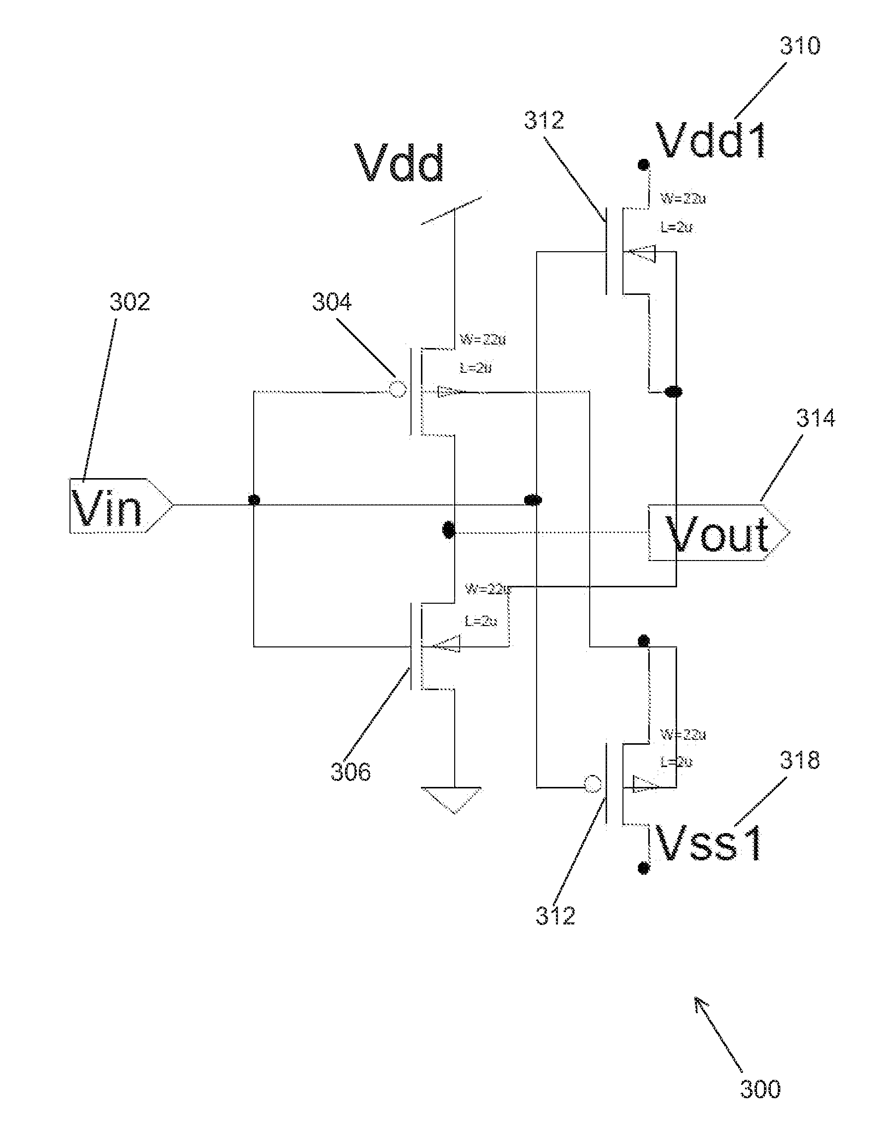
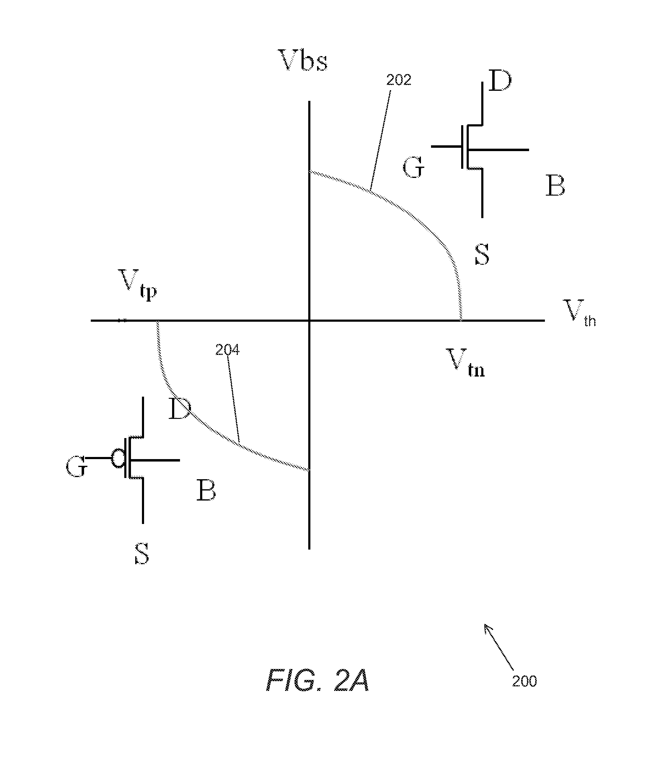
Systems and methods for dynamic mosfet body biasing for low power, fast response VLSI applications
PatentInactiveUS20120206188A1
Innovation
- Adjusting the voltage applied to the body terminal of MOSFET transistors (Vbs) to control the threshold voltage (Vth), dynamically biasing it to minimize leakage current and enhance response time by using control circuitry to apply different voltages based on the transistor's operational state.

MOS transistor with a controlled threshold voltage
PatentInactiveUS6989569B1
Innovation
- The introduction of an Electrically Induced Body (EIB) MOS transistor with a substrate voltage applied to induce charges, creating a depletion layer depth corresponding to the single crystal layer thickness, allowing for a larger body effect factor without increasing impurity concentration, thereby enabling faster operation and reduced power consumption.


Quantum Computing Hardware Standards and Regulations
The quantum computing industry currently operates under a fragmented regulatory landscape, with various national and international bodies working to establish comprehensive standards for hardware components, particularly for high-speed VLSI transistors used in quantum systems. The IEEE Quantum Computing Standards Committee has initiated several working groups focused on defining performance benchmarks and safety protocols for quantum hardware, while the International Organization for Standardization (ISO) is developing ISO/IEC 23053 standards specifically addressing quantum computing terminology and hardware specifications.
Current regulatory frameworks primarily focus on electromagnetic compatibility (EMC) standards, as quantum systems require extremely low noise environments where traditional VLSI switching speeds can introduce interference. The Federal Communications Commission (FCC) and European Telecommunications Standards Institute (ETSI) have established specific guidelines for quantum computing facilities, mandating strict electromagnetic shielding requirements and frequency allocation protocols that directly impact transistor design specifications.
Safety regulations governing cryogenic operations significantly influence VLSI transistor implementation in quantum systems. The Occupational Safety and Health Administration (OSHA) and equivalent international bodies have established protocols for ultra-low temperature environments, requiring specialized transistor packaging and thermal management systems. These regulations mandate fail-safe mechanisms and redundant control systems, directly affecting switching speed optimization strategies and circuit design approaches.
Export control regulations, particularly the International Traffic in Arms Regulations (ITAR) and Export Administration Regulations (EAR), classify advanced quantum computing hardware as dual-use technology. This classification impacts the development and distribution of high-performance VLSI transistors, requiring manufacturers to implement specific design documentation, supply chain verification, and technology transfer protocols that can influence development timelines and technical specifications.
Emerging standards from the National Institute of Standards and Technology (NIST) Post-Quantum Cryptography initiative are establishing new requirements for quantum-resistant hardware implementations. These standards necessitate specific transistor switching characteristics to support quantum error correction protocols and fault-tolerant computing architectures, creating new performance benchmarks that extend beyond traditional speed metrics to include coherence preservation and quantum state fidelity maintenance.
Cryogenic Operating Challenges for VLSI Components
Quantum computing systems operate at extremely low temperatures, typically in the millikelvin range, to maintain quantum coherence and minimize thermal noise. This cryogenic environment presents unprecedented challenges for VLSI components that must interface with quantum processors. Traditional semiconductor devices experience dramatic changes in electrical characteristics as temperatures approach absolute zero, fundamentally altering their switching behavior and performance metrics.
At cryogenic temperatures, carrier mobility in silicon increases significantly due to reduced phonon scattering, while threshold voltages shift substantially. These changes create both opportunities and obstacles for transistor switching speed optimization. While higher carrier mobility theoretically enables faster switching, the accompanying threshold voltage variations can lead to unpredictable circuit behavior and timing inconsistencies across different operating conditions.
Thermal management becomes critically important as even minimal heat generation from VLSI components can disrupt the delicate quantum states. Power dissipation constraints in cryogenic environments are orders of magnitude more stringent than room temperature applications, as cooling power at millikelvin temperatures requires enormous energy expenditure. This necessitates ultra-low-power circuit designs that maintain high switching speeds while generating minimal heat.
Material properties undergo significant transformations at cryogenic temperatures, affecting interconnect resistance, dielectric constants, and mechanical stress within integrated circuits. Metal interconnects exhibit reduced resistance, potentially improving signal propagation speeds, but thermal expansion mismatches can create reliability issues. Gate oxide behavior changes substantially, affecting capacitance values and leakage currents that directly impact switching characteristics.
Packaging and interconnection technologies face unique challenges in cryogenic quantum computing applications. Traditional packaging materials may become brittle or exhibit poor thermal conductivity at extremely low temperatures. Signal integrity issues become more pronounced due to impedance variations and potential superconducting effects in certain materials, requiring specialized design considerations for maintaining reliable high-speed switching operations.
The integration of classical VLSI control electronics with quantum processors demands innovative approaches to address temperature gradients and thermal isolation requirements. Developing transistor technologies that can operate efficiently across the temperature range from room temperature to millikelvin conditions while maintaining consistent switching performance represents a fundamental engineering challenge for advancing quantum computing systems.
Unlock deeper insights with PatSnap Eureka Quick Research — get a full tech report to explore trends and direct your research. Try now!
Generate Your Research Report Instantly with AI Agent
Supercharge your innovation with PatSnap Eureka AI Agent Platform!