Improving Circuit Pattern Uniformity in Substrate-Like PCBs
APR 22, 20269 MIN READ
Generate Your Research Report Instantly with AI Agent
PatSnap Eureka helps you evaluate technical feasibility & market potential.
Substrate-Like PCB Pattern Uniformity Background and Objectives
Substrate-like PCBs represent a critical evolution in electronic packaging technology, bridging the gap between traditional printed circuit boards and advanced semiconductor substrates. These high-density interconnect structures feature ultra-fine line widths, microvias, and complex multilayer architectures that enable miniaturization of electronic devices while maintaining superior electrical performance. The substrate-like approach incorporates advanced materials and manufacturing processes typically associated with IC packaging into PCB fabrication.
The historical development of substrate-like PCBs emerged from the semiconductor industry's need for higher integration density and improved signal integrity. Early implementations in the 1990s focused on mobile device applications, where space constraints demanded innovative packaging solutions. The technology has since evolved through multiple generations, incorporating build-up layer technologies, embedded components, and advanced via formation techniques.
Current market drivers include the proliferation of 5G communications, artificial intelligence processors, and Internet of Things devices, all requiring compact, high-performance interconnect solutions. The automotive electronics sector has also become a significant adopter, particularly for advanced driver assistance systems and electric vehicle power management applications.
Pattern uniformity challenges in substrate-like PCBs stem from the inherent complexity of manufacturing processes involving multiple photolithography steps, chemical etching, and layer lamination. Variations in line width, spacing, and via formation across the substrate surface directly impact electrical performance, signal integrity, and manufacturing yield. These non-uniformities can cause impedance mismatches, crosstalk, and reliability issues in high-frequency applications.
The primary technical objectives focus on achieving consistent pattern dimensions across entire substrate panels, minimizing process-induced variations, and establishing robust manufacturing controls. Target specifications typically include line width variations within ±10% across the substrate area, via diameter consistency within ±5 micrometers, and layer-to-layer registration accuracy better than ±15 micrometers.
Advanced metrology and process control systems are essential for monitoring and correcting pattern uniformity deviations in real-time. The integration of machine learning algorithms for predictive process optimization represents a key technological advancement, enabling proactive adjustment of manufacturing parameters to maintain uniformity standards throughout production runs.
Market Demand for High-Precision Substrate-Like PCBs
The global electronics industry is experiencing unprecedented demand for high-precision substrate-like PCBs, driven by the rapid advancement of consumer electronics, automotive systems, and telecommunications infrastructure. Modern electronic devices require increasingly compact designs with enhanced performance capabilities, creating substantial market pressure for PCBs that can deliver superior circuit pattern uniformity and reliability.
The smartphone and tablet markets represent the largest demand segment for high-precision substrate-like PCBs. These devices require ultra-thin form factors while maintaining complex multilayer circuit architectures. Manufacturers are seeking PCB solutions that can accommodate high-density interconnects with minimal signal interference, making circuit pattern uniformity a critical performance parameter. The transition to 5G technology has further intensified these requirements, as radio frequency components demand exceptional precision in circuit geometry.
Automotive electronics constitute another rapidly expanding market segment. The proliferation of advanced driver assistance systems, electric vehicle powertrains, and autonomous driving technologies has created substantial demand for substrate-like PCBs capable of operating under harsh environmental conditions. These applications require consistent circuit patterns to ensure reliable performance across temperature variations and mechanical stress, making uniformity improvements essential for automotive qualification standards.
Data center and cloud computing infrastructure represent high-value market opportunities for precision PCB manufacturers. Server motherboards, network switches, and storage systems require substrate-like PCBs with exceptional signal integrity characteristics. The increasing data processing demands and higher operating frequencies necessitate improved circuit pattern uniformity to minimize electromagnetic interference and signal degradation.
The aerospace and defense sectors continue to drive demand for the highest precision substrate-like PCBs. These applications often require custom solutions with stringent uniformity specifications, creating opportunities for manufacturers capable of delivering advanced circuit pattern control. Military and space applications particularly value reliability and performance consistency, making uniformity improvements directly translatable to market advantages.
Emerging technologies including artificial intelligence accelerators, quantum computing peripherals, and advanced medical devices are creating new market segments with demanding precision requirements. These applications often require substrate-like PCBs with novel material combinations and specialized manufacturing processes, presenting opportunities for companies that can master circuit pattern uniformity challenges.
Current Challenges in Circuit Pattern Uniformity Control
Circuit pattern uniformity in substrate-like PCBs faces significant manufacturing challenges that stem from the inherent complexity of multi-layer structures and the demanding precision requirements of modern electronic applications. The primary obstacle lies in achieving consistent trace width, spacing, and thickness across different layers while maintaining electrical performance specifications.
Manufacturing process variations represent a critical challenge in pattern uniformity control. Photolithography processes suffer from exposure dose variations, mask alignment errors, and resist thickness inconsistencies that directly impact pattern fidelity. These variations become more pronounced as feature sizes decrease and layer counts increase, particularly in high-density interconnect designs where tolerances are measured in micrometers.
Etching process control presents another substantial hurdle. Chemical etching rates vary across the substrate surface due to solution concentration gradients, temperature variations, and agitation differences. This results in non-uniform conductor widths and can cause impedance mismatches that degrade signal integrity. The challenge intensifies with complex geometries where different pattern densities on the same layer experience varying etch rates.
Material property variations significantly impact pattern uniformity. Substrate materials exhibit thickness variations, dielectric constant fluctuations, and thermal expansion coefficient differences that affect pattern registration between layers. Copper foil thickness variations and surface roughness inconsistencies further complicate achieving uniform electrical characteristics across the entire substrate area.
Thermal management during processing creates additional uniformity challenges. Temperature gradients during lamination, curing, and drilling operations cause differential expansion and contraction, leading to pattern distortion and layer misalignment. These thermal effects are particularly problematic in large substrate formats where temperature uniformity becomes increasingly difficult to maintain.
Advanced packaging requirements have intensified these challenges. Fine-pitch components, embedded components, and high-frequency applications demand tighter tolerances that push current manufacturing capabilities to their limits. The need for consistent impedance control, minimal crosstalk, and reliable via connections requires unprecedented levels of pattern uniformity that existing processes struggle to achieve consistently.
Quality control and measurement limitations compound these manufacturing challenges. Traditional inspection methods lack the resolution and throughput necessary to detect subtle pattern variations that can significantly impact electrical performance. Real-time process monitoring capabilities remain insufficient for implementing effective closed-loop control systems that could compensate for process variations during manufacturing.
Existing Solutions for Pattern Uniformity Enhancement
01 Photolithography process optimization for pattern uniformity
Advanced photolithography techniques are employed to achieve uniform circuit patterns on substrate-like PCBs. This includes optimizing exposure parameters, developing precise mask alignment methods, and controlling light intensity distribution across the substrate surface. The process ensures consistent pattern transfer with minimal dimensional variations across different regions of the PCB, resulting in improved electrical performance and reliability.- Photolithography process optimization for pattern uniformity: Advanced photolithography techniques are employed to achieve uniform circuit patterns on substrate-like PCBs. This includes optimizing exposure parameters, developing precise mask alignment methods, and controlling light intensity distribution across the substrate surface. The process ensures consistent pattern transfer and minimizes variations in line width and spacing across different regions of the PCB. Enhanced photoresist application and development procedures contribute to improved pattern fidelity and uniformity.
- Etching process control for uniform circuit formation: Precise control of etching parameters is critical for achieving uniform circuit patterns. This involves optimizing etchant composition, temperature, and flow rate to ensure consistent material removal across the entire substrate. Advanced etching techniques include plasma etching and wet chemical etching with real-time monitoring systems. The methods address issues such as over-etching and under-etching in different areas, resulting in uniform conductor width and spacing throughout the PCB.
- Substrate surface treatment and preparation methods: Surface treatment techniques are applied to enhance pattern uniformity on substrate-like PCBs. These methods include surface cleaning, roughening, and coating processes that create a uniform base for circuit pattern formation. The treatments improve adhesion between the substrate and conductive layers while minimizing surface irregularities. Specialized preparation procedures ensure consistent surface properties across the entire substrate area, which is essential for achieving uniform pattern transfer and reducing defects.
- Plating and metallization uniformity control: Advanced plating techniques are utilized to achieve uniform metal deposition for circuit patterns on substrate-like PCBs. This includes electroplating and electroless plating processes with controlled current density distribution and chemical bath composition. The methods ensure consistent metal thickness across the substrate surface, preventing variations that could affect circuit performance. Process parameters such as plating time, temperature, and agitation are optimized to achieve uniform conductor formation and minimize thickness variations between different circuit areas.
- Inspection and measurement systems for pattern uniformity verification: Automated inspection and measurement systems are implemented to verify and ensure circuit pattern uniformity on substrate-like PCBs. These systems utilize optical inspection, scanning electron microscopy, and dimensional measurement techniques to detect variations in pattern geometry. Real-time monitoring and feedback control mechanisms enable immediate process adjustments to maintain uniformity standards. The inspection methods can identify defects such as line width variations, spacing irregularities, and alignment errors across the entire substrate area, ensuring consistent quality control.
02 Etching process control for uniform circuit formation
Precise control of etching parameters is critical for achieving uniform circuit patterns. This involves optimizing etchant composition, temperature, flow rate, and etching time to ensure consistent material removal across the entire substrate. Advanced monitoring systems and feedback mechanisms are implemented to maintain uniformity during the etching process, preventing over-etching or under-etching in different areas of the PCB.Expand Specific Solutions03 Substrate surface treatment and preparation methods
Surface treatment techniques are applied to enhance pattern uniformity on substrate-like PCBs. These methods include surface cleaning, roughening, and coating processes that create a uniform base layer for subsequent circuit pattern formation. The treatments ensure consistent adhesion properties and surface characteristics across the entire substrate, which is essential for achieving uniform pattern transfer and preventing defects.Expand Specific Solutions04 Plating and metallization uniformity control
Electroplating and metallization processes are optimized to achieve uniform metal deposition across circuit patterns. This includes controlling current density distribution, plating solution composition, and agitation methods to ensure consistent metal thickness and quality throughout the substrate. Advanced plating techniques such as pulse plating and additive control are utilized to minimize thickness variations and improve pattern uniformity.Expand Specific Solutions05 Inspection and measurement systems for pattern uniformity verification
Automated optical inspection and measurement systems are implemented to verify and ensure circuit pattern uniformity across substrate-like PCBs. These systems utilize advanced imaging technologies, pattern recognition algorithms, and statistical analysis methods to detect dimensional variations, defects, and non-uniformities. Real-time monitoring and feedback control enable immediate process adjustments to maintain consistent pattern quality throughout production.Expand Specific Solutions
Key Players in Advanced PCB and Substrate Manufacturing
The substrate-like PCB circuit pattern uniformity technology represents a mature market segment within the broader electronics manufacturing industry, currently experiencing steady growth driven by 5G infrastructure, automotive electronics, and high-performance computing demands. The competitive landscape is dominated by established players across three key regions: Asian manufacturers like Samsung Electro-Mechanics, TSMC, and SK Hynix lead in advanced substrate technologies and high-volume production capabilities; Chinese companies including Shenzhen Fastprint Circuit Tech, WUS Printed Circuit, and Victory Giant Technology focus on cost-effective solutions and rapid prototyping services; while global equipment suppliers such as Applied Materials, Tokyo Electron, and Texas Instruments provide critical manufacturing tools and process technologies. The technology maturity varies significantly, with tier-one players achieving advanced HDI and IC substrate capabilities, while emerging manufacturers concentrate on standard multilayer PCB solutions, creating a multi-tiered competitive structure that serves diverse market segments from consumer electronics to aerospace applications.
Samsung Electro-Mechanics Co., Ltd.
Technical Solution: Samsung Electro-Mechanics employs advanced substrate-like PCB manufacturing technologies including modified semi-additive processes (mSAP) and panel-level packaging approaches to improve circuit pattern uniformity. Their solution integrates precise copper plating control systems with real-time thickness monitoring to maintain consistent trace widths across large substrate areas. The company utilizes multi-step lithography processes combined with optimized etching parameters to achieve uniform line/space patterns. Additionally, they implement advanced surface treatment techniques and controlled impedance matching to ensure electrical performance consistency throughout the substrate.
Strengths: Strong integration capabilities with semiconductor packaging, advanced manufacturing infrastructure. Weaknesses: Higher cost structure, limited flexibility for custom applications.
Taiwan Semiconductor Manufacturing Co., Ltd.
Technical Solution: TSMC's approach to circuit pattern uniformity in substrate-like PCBs focuses on their Integrated Fan-Out (InFO) and Chip-on-Wafer-on-Substrate (CoWoS) technologies. They employ sophisticated process control systems that monitor and adjust lithography exposure parameters in real-time to maintain pattern fidelity across wafer-level substrates. Their solution includes advanced overlay control systems, optimized resist processing, and precision etching techniques that ensure uniform circuit patterns even at fine pitches below 10 micrometers. TSMC also utilizes computational lithography and machine learning algorithms to predict and compensate for pattern variations before they occur in production.
Strengths: Leading-edge process technology, excellent yield control, strong R&D capabilities. Weaknesses: High capital requirements, focus primarily on high-volume applications.
Core Innovations in Circuit Pattern Control Technologies
Printed circuit board and method of manufacturing the same
PatentInactiveUS20120125667A1
Innovation
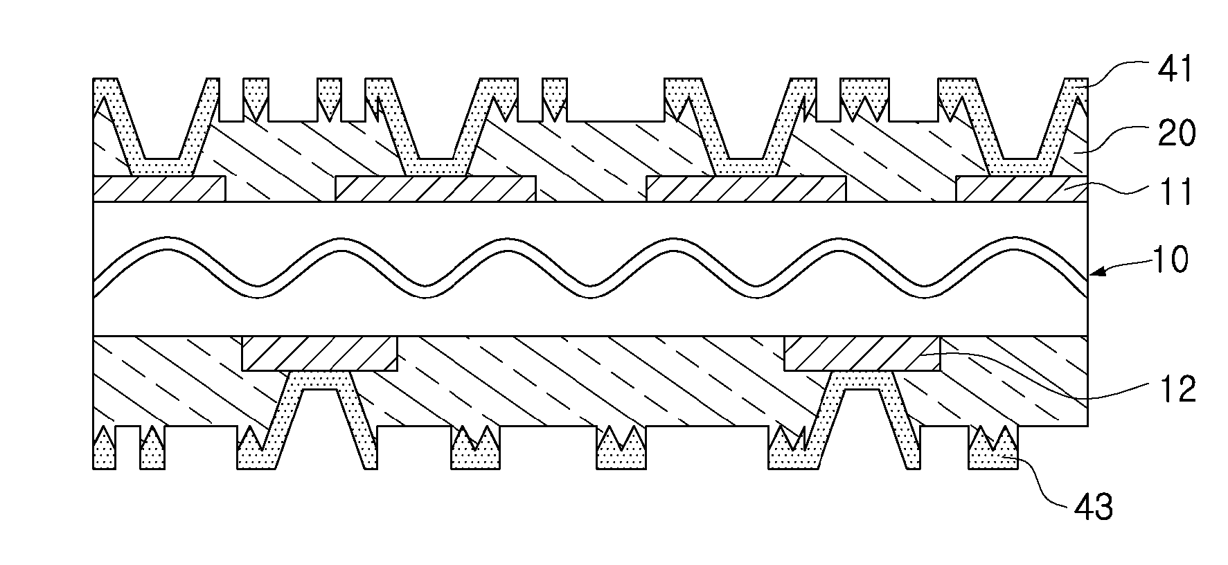
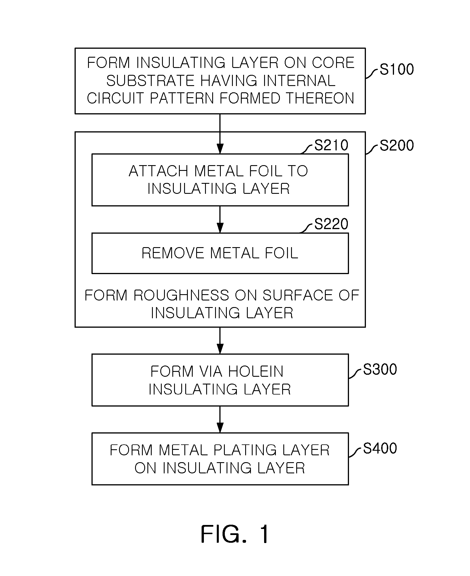
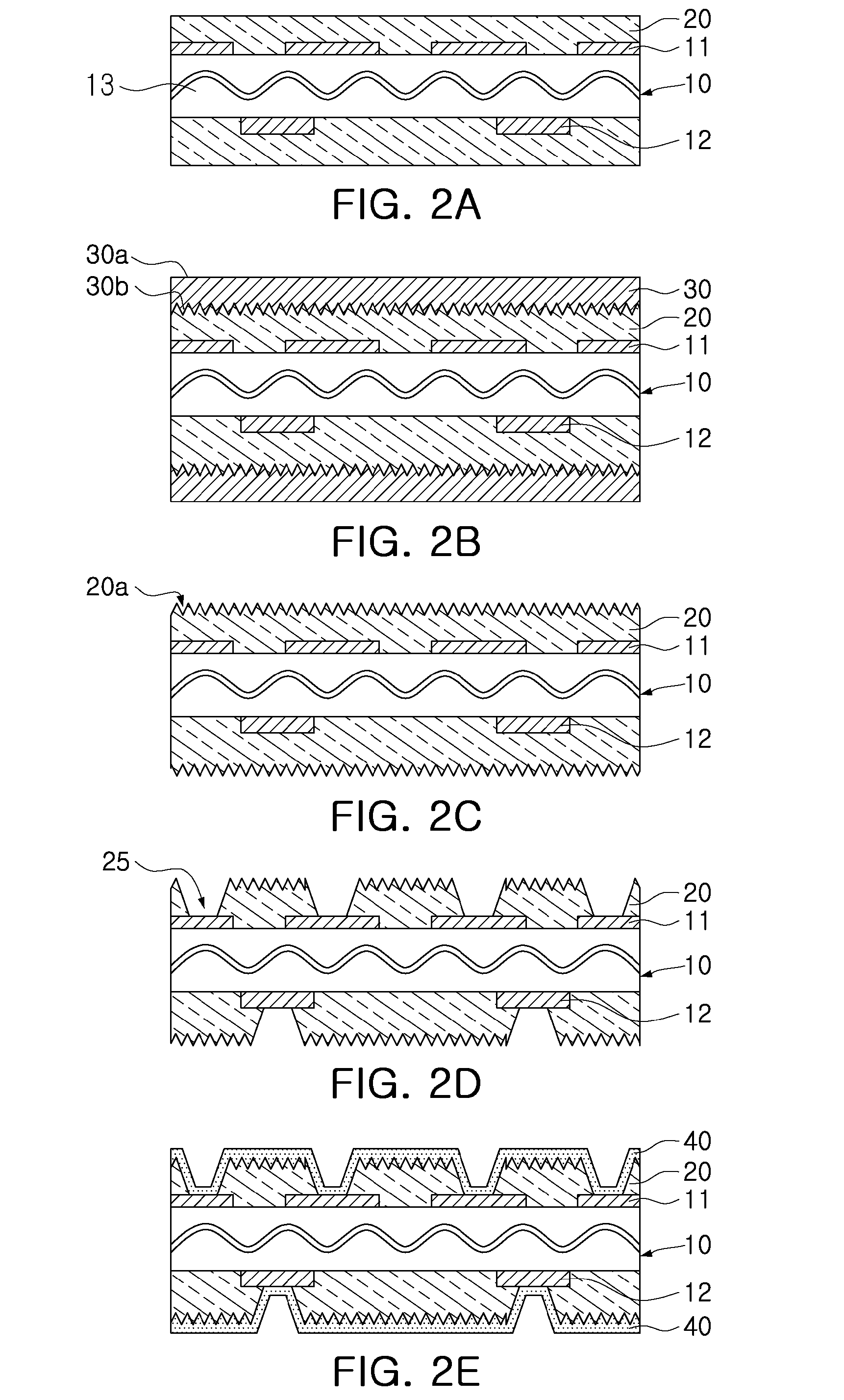
- A printed circuit board with a core substrate and an insulating layer featuring uniform nanoscale roughness, where a metal foil with controlled roughness is attached and then removed to form a conductive layer, allowing for the creation of fine circuit patterns through semi-additive or modified semi-additive processes, ensuring strong adhesion and precise line/space intervals.

Printed circuit board
PatentActiveUS20220061147A1
Innovation
- A printed circuit board with a circuit pattern that controls surface roughness across multiple surfaces, maintaining Ra values between 0.1 μm to 0.31 μm and Rq values of 0.42 μm or less, ensuring that surface roughness varies based on surface length, thereby minimizing signal loss by reducing resistance during high-frequency signal transmission.


Manufacturing Process Optimization Strategies
Manufacturing process optimization for substrate-like PCBs requires a systematic approach that addresses multiple production variables simultaneously. The primary focus centers on achieving consistent circuit pattern uniformity through precise control of fabrication parameters, material handling procedures, and quality assurance protocols. Advanced process optimization strategies integrate real-time monitoring systems with predictive analytics to minimize variations in pattern formation and ensure reproducible manufacturing outcomes.
Temperature control optimization represents a critical manufacturing parameter that directly impacts circuit pattern uniformity. Implementing zone-based thermal management systems allows for precise temperature regulation during lamination, etching, and curing processes. Advanced thermal profiling techniques enable manufacturers to establish optimal temperature gradients that promote uniform material flow and prevent localized heating effects that can cause pattern distortions. Multi-point temperature monitoring with feedback control systems ensures consistent thermal conditions across the entire substrate surface.
Chemical process optimization focuses on achieving uniform distribution of etching solutions, plating chemicals, and cleaning agents throughout the manufacturing sequence. Flow dynamics modeling helps optimize chemical delivery systems to ensure consistent concentration levels and contact times across all circuit areas. Automated chemical replenishment systems maintain optimal solution properties while reducing batch-to-batch variations that can affect pattern quality.
Equipment calibration and maintenance protocols form the foundation of consistent manufacturing performance. Regular calibration of imaging systems, exposure equipment, and measurement tools ensures accurate pattern transfer and dimensional control. Preventive maintenance schedules minimize equipment drift and maintain optimal operating conditions. Statistical process control methods track equipment performance metrics and identify potential issues before they impact product quality.
Material handling optimization addresses substrate preparation, storage conditions, and processing sequence management. Controlled environment storage prevents material degradation and moisture absorption that can affect pattern formation. Automated material handling systems reduce human error and ensure consistent processing conditions. Batch tracking systems maintain traceability and enable rapid identification of process variations that may impact circuit pattern uniformity across production runs.
Quality Control Standards for Substrate-Like PCB Applications
Quality control standards for substrate-like PCB applications represent a critical framework for ensuring consistent circuit pattern uniformity across manufacturing processes. These standards encompass dimensional tolerances, electrical performance criteria, and visual inspection requirements that directly impact the reliability of high-density interconnect structures. The establishment of comprehensive quality metrics addresses the unique challenges posed by substrate-like PCBs, where traditional PCB manufacturing tolerances may prove insufficient for advanced packaging applications.
International standards organizations have developed specific guidelines for substrate-like PCB quality assessment, including IPC-6012 Class 3+ requirements and JEDEC standards for semiconductor packaging substrates. These frameworks define acceptable limits for line width variation, typically maintaining ±10% tolerance for critical signal traces, while via registration accuracy must remain within ±25 micrometers. Surface roughness specifications ensure optimal signal integrity, with Ra values typically constrained below 0.5 micrometers for high-frequency applications.
Statistical process control methodologies form the backbone of effective quality management in substrate-like PCB manufacturing. Implementation of Six Sigma principles enables manufacturers to achieve defect rates below 3.4 parts per million, essential for automotive and aerospace applications. Real-time monitoring systems track key parameters including etch uniformity, plating thickness variation, and lamination pressure distribution across panel surfaces.
Advanced metrology techniques support quality control implementation through automated optical inspection systems capable of detecting pattern deviations as small as 2 micrometers. X-ray inspection protocols verify internal via structures and buried interconnects, while electrical testing validates impedance consistency within ±5% tolerance bands. Cross-sectional analysis provides verification of layer-to-layer registration accuracy and dielectric thickness uniformity.
Traceability requirements mandate comprehensive documentation of manufacturing parameters, material lot numbers, and process conditions for each production batch. This data enables rapid root cause analysis when quality deviations occur and supports continuous improvement initiatives. Integration with manufacturing execution systems ensures real-time quality data collection and automated rejection of non-conforming units before downstream processing.
Unlock deeper insights with PatSnap Eureka Quick Research — get a full tech report to explore trends and direct your research. Try now!
Generate Your Research Report Instantly with AI Agent
Supercharge your innovation with PatSnap Eureka AI Agent Platform!