

Improving Copper Clip Bonding for Thin Substrates: Key Challenges and Solutions
MAY 22, 20269 MIN READ
Generate Your Research Report Instantly with AI Agent
PatSnap Eureka helps you evaluate technical feasibility & market potential.
Copper Clip Bonding Technology Background and Objectives
Copper clip bonding technology has emerged as a critical interconnection method in advanced semiconductor packaging, particularly for power electronics and high-performance computing applications. This technology represents a significant evolution from traditional wire bonding approaches, offering superior electrical and thermal performance through the use of copper clips as interconnect elements between semiconductor dies and substrates.
The historical development of copper clip bonding can be traced back to the early 2000s when the semiconductor industry began seeking alternatives to aluminum wire bonding for high-power applications. The technology gained momentum as power semiconductor devices required enhanced current-carrying capacity and improved thermal dissipation. Unlike conventional wire bonds, copper clips provide larger cross-sectional areas and shorter electrical paths, resulting in reduced parasitic inductance and resistance.
The evolution of this technology has been driven by the increasing demands of modern electronic systems, particularly in automotive, industrial, and renewable energy sectors. As power densities continue to rise and device miniaturization progresses, the limitations of traditional bonding methods have become more apparent, necessitating the adoption of advanced interconnection solutions.
Current technological trends indicate a strong shift toward thinner substrates in semiconductor packaging, driven by the need for compact, lightweight, and high-performance electronic devices. However, this trend presents significant challenges for copper clip bonding processes. Thin substrates, typically ranging from 50 to 200 micrometers in thickness, are inherently more susceptible to mechanical stress, thermal warpage, and processing-induced damage during bonding operations.
The primary objective of advancing copper clip bonding technology for thin substrates centers on achieving reliable, high-yield interconnections while maintaining substrate integrity throughout the manufacturing process. This involves developing optimized bonding parameters, including precise control of bonding force, temperature profiles, and ultrasonic energy application to ensure adequate metallurgical bonding without causing substrate cracking or delamination.
Furthermore, the technology aims to establish robust process windows that accommodate the inherent variability in thin substrate properties while delivering consistent bonding quality. The ultimate goal encompasses enabling next-generation semiconductor packages that leverage the benefits of both copper clip interconnections and thin substrate architectures, thereby supporting the continued advancement of high-performance, miniaturized electronic systems across various industrial applications.
The historical development of copper clip bonding can be traced back to the early 2000s when the semiconductor industry began seeking alternatives to aluminum wire bonding for high-power applications. The technology gained momentum as power semiconductor devices required enhanced current-carrying capacity and improved thermal dissipation. Unlike conventional wire bonds, copper clips provide larger cross-sectional areas and shorter electrical paths, resulting in reduced parasitic inductance and resistance.
The evolution of this technology has been driven by the increasing demands of modern electronic systems, particularly in automotive, industrial, and renewable energy sectors. As power densities continue to rise and device miniaturization progresses, the limitations of traditional bonding methods have become more apparent, necessitating the adoption of advanced interconnection solutions.
Current technological trends indicate a strong shift toward thinner substrates in semiconductor packaging, driven by the need for compact, lightweight, and high-performance electronic devices. However, this trend presents significant challenges for copper clip bonding processes. Thin substrates, typically ranging from 50 to 200 micrometers in thickness, are inherently more susceptible to mechanical stress, thermal warpage, and processing-induced damage during bonding operations.
The primary objective of advancing copper clip bonding technology for thin substrates centers on achieving reliable, high-yield interconnections while maintaining substrate integrity throughout the manufacturing process. This involves developing optimized bonding parameters, including precise control of bonding force, temperature profiles, and ultrasonic energy application to ensure adequate metallurgical bonding without causing substrate cracking or delamination.
Furthermore, the technology aims to establish robust process windows that accommodate the inherent variability in thin substrate properties while delivering consistent bonding quality. The ultimate goal encompasses enabling next-generation semiconductor packages that leverage the benefits of both copper clip interconnections and thin substrate architectures, thereby supporting the continued advancement of high-performance, miniaturized electronic systems across various industrial applications.
Market Demand for Thin Substrate Copper Clip Solutions
The semiconductor packaging industry is experiencing unprecedented demand for thin substrate copper clip bonding solutions, driven by the relentless pursuit of miniaturization and enhanced performance in electronic devices. Consumer electronics manufacturers are increasingly adopting ultra-thin form factors to meet market expectations for sleeker smartphones, tablets, and wearable devices, creating substantial pressure on packaging technologies to deliver reliable interconnection solutions within severely constrained vertical spaces.
Automotive electronics represents another significant growth driver, particularly with the accelerating adoption of electric vehicles and advanced driver assistance systems. These applications demand robust thermal management capabilities while maintaining compact packaging profiles, making copper clip bonding on thin substrates an essential technology for power semiconductor modules and high-frequency communication components.
The 5G infrastructure rollout has intensified demand for high-performance RF components that require superior electrical conductivity and thermal dissipation properties. Copper clip bonding technology addresses these requirements effectively, offering lower parasitic inductance and enhanced current-carrying capacity compared to traditional wire bonding approaches, particularly crucial for millimeter-wave applications and base station equipment.
Data center and cloud computing infrastructure expansion continues to fuel demand for high-density packaging solutions. Server processors and memory modules increasingly rely on thin substrate technologies to achieve optimal performance per unit volume, with copper clip bonding enabling efficient heat removal from densely packed semiconductor dies while maintaining signal integrity at high frequencies.
Industrial IoT applications and edge computing devices represent emerging market segments where space constraints and reliability requirements converge. These applications often operate in harsh environmental conditions, necessitating robust interconnection technologies that can withstand thermal cycling and mechanical stress while occupying minimal board real estate.
The market trajectory indicates sustained growth potential, with packaging density requirements continuing to tighten across all application segments. Manufacturers are actively seeking solutions that can accommodate substrate thicknesses below traditional limits while maintaining manufacturing yield and long-term reliability standards, positioning advanced copper clip bonding technologies as critical enablers for next-generation electronic systems.
Automotive electronics represents another significant growth driver, particularly with the accelerating adoption of electric vehicles and advanced driver assistance systems. These applications demand robust thermal management capabilities while maintaining compact packaging profiles, making copper clip bonding on thin substrates an essential technology for power semiconductor modules and high-frequency communication components.
The 5G infrastructure rollout has intensified demand for high-performance RF components that require superior electrical conductivity and thermal dissipation properties. Copper clip bonding technology addresses these requirements effectively, offering lower parasitic inductance and enhanced current-carrying capacity compared to traditional wire bonding approaches, particularly crucial for millimeter-wave applications and base station equipment.
Data center and cloud computing infrastructure expansion continues to fuel demand for high-density packaging solutions. Server processors and memory modules increasingly rely on thin substrate technologies to achieve optimal performance per unit volume, with copper clip bonding enabling efficient heat removal from densely packed semiconductor dies while maintaining signal integrity at high frequencies.
Industrial IoT applications and edge computing devices represent emerging market segments where space constraints and reliability requirements converge. These applications often operate in harsh environmental conditions, necessitating robust interconnection technologies that can withstand thermal cycling and mechanical stress while occupying minimal board real estate.
The market trajectory indicates sustained growth potential, with packaging density requirements continuing to tighten across all application segments. Manufacturers are actively seeking solutions that can accommodate substrate thicknesses below traditional limits while maintaining manufacturing yield and long-term reliability standards, positioning advanced copper clip bonding technologies as critical enablers for next-generation electronic systems.
Current Challenges in Copper Clip Bonding on Thin Substrates
Copper clip bonding on thin substrates faces significant thermal management challenges due to the inherent thermal mismatch between materials. The coefficient of thermal expansion (CTE) difference between copper clips and thin substrate materials creates substantial stress concentrations during temperature cycling. This thermal stress can lead to delamination, crack propagation, and eventual bond failure, particularly at the interface between the copper clip and the substrate surface.
The mechanical integrity of bonded joints becomes increasingly compromised as substrate thickness decreases. Thin substrates exhibit reduced structural rigidity, making them susceptible to warpage and flexural deformation during the bonding process. This substrate flexibility can result in non-uniform pressure distribution across the bonding interface, leading to inconsistent bond quality and potential void formation. The reduced mechanical support also amplifies the impact of external stresses on the bonded assembly.
Process control presents another critical challenge in achieving reliable copper clip bonding on thin substrates. Traditional bonding parameters optimized for thicker substrates often prove inadequate for thin substrate applications. The reduced thermal mass of thin substrates leads to rapid temperature fluctuations during heating and cooling cycles, making precise temperature control extremely difficult. Additionally, the application of bonding pressure must be carefully calibrated to avoid substrate damage while ensuring adequate interfacial contact.
Interface contamination and surface preparation issues are magnified in thin substrate applications. The reduced substrate thickness limits the available surface area for effective cleaning and preparation procedures. Organic residues, oxide layers, and moisture absorption can significantly impact bond strength and reliability. The challenge is further complicated by the need to maintain substrate integrity during aggressive surface preparation processes.
Electrical performance degradation represents a growing concern as substrate thickness decreases. Parasitic inductance and resistance effects become more pronounced in thin substrate configurations, potentially compromising the electrical benefits that copper clip bonding is intended to provide. The reduced current-carrying capacity and increased susceptibility to electromagnetic interference pose additional challenges for high-performance applications requiring optimal electrical characteristics.
The mechanical integrity of bonded joints becomes increasingly compromised as substrate thickness decreases. Thin substrates exhibit reduced structural rigidity, making them susceptible to warpage and flexural deformation during the bonding process. This substrate flexibility can result in non-uniform pressure distribution across the bonding interface, leading to inconsistent bond quality and potential void formation. The reduced mechanical support also amplifies the impact of external stresses on the bonded assembly.
Process control presents another critical challenge in achieving reliable copper clip bonding on thin substrates. Traditional bonding parameters optimized for thicker substrates often prove inadequate for thin substrate applications. The reduced thermal mass of thin substrates leads to rapid temperature fluctuations during heating and cooling cycles, making precise temperature control extremely difficult. Additionally, the application of bonding pressure must be carefully calibrated to avoid substrate damage while ensuring adequate interfacial contact.
Interface contamination and surface preparation issues are magnified in thin substrate applications. The reduced substrate thickness limits the available surface area for effective cleaning and preparation procedures. Organic residues, oxide layers, and moisture absorption can significantly impact bond strength and reliability. The challenge is further complicated by the need to maintain substrate integrity during aggressive surface preparation processes.
Electrical performance degradation represents a growing concern as substrate thickness decreases. Parasitic inductance and resistance effects become more pronounced in thin substrate configurations, potentially compromising the electrical benefits that copper clip bonding is intended to provide. The reduced current-carrying capacity and increased susceptibility to electromagnetic interference pose additional challenges for high-performance applications requiring optimal electrical characteristics.
Existing Copper Clip Bonding Solutions for Thin Substrates
01 Copper clip bonding process optimization and control methods
Various methods and techniques for optimizing the copper clip bonding process to ensure high-quality connections. This includes controlling bonding parameters such as temperature, pressure, and time to achieve optimal bond strength and reliability. Process monitoring and feedback systems are employed to maintain consistent bonding quality throughout manufacturing.- Copper clip bonding process optimization and control methods: Various methods and techniques for optimizing the copper clip bonding process to ensure high-quality connections. This includes controlling bonding parameters such as temperature, pressure, and time to achieve optimal bond strength and reliability. Process monitoring and feedback systems are employed to maintain consistent bonding quality throughout manufacturing.
- Copper clip design and structural configurations for enhanced bonding: Innovative copper clip designs and structural modifications that improve bonding performance and reliability. This includes optimized clip geometries, surface treatments, and material compositions that enhance the mechanical and electrical properties of the bond interface. Special attention is given to stress distribution and thermal management in the bonded assembly.
- Quality assessment and testing methods for copper clip bonds: Comprehensive testing methodologies and quality assessment techniques for evaluating copper clip bonding quality. This encompasses non-destructive testing methods, mechanical strength evaluation, electrical performance testing, and reliability assessment under various environmental conditions. Advanced inspection techniques are used to detect defects and ensure bond integrity.
- Equipment and tooling for copper clip bonding applications: Specialized equipment, tooling, and apparatus designed for copper clip bonding operations. This includes bonding machines, fixtures, heating systems, and automated handling equipment that ensure precise positioning and consistent bonding conditions. The equipment is designed to accommodate various clip sizes and configurations while maintaining high throughput and quality standards.
- Materials and surface preparation for improved copper clip bonding: Advanced materials, coatings, and surface preparation techniques that enhance copper clip bonding quality and durability. This includes surface cleaning methods, flux applications, protective coatings, and material compatibility considerations. Special emphasis is placed on preventing oxidation, improving wettability, and ensuring long-term bond stability under operational conditions.
02 Copper clip design and structural configurations for enhanced bonding
Innovative copper clip designs and structural modifications that improve bonding performance and reliability. This includes optimized clip geometries, surface treatments, and material compositions that enhance the mechanical and electrical properties of the bond interface. Special attention is given to stress distribution and thermal management in the bonded structure.Expand Specific Solutions03 Quality assessment and testing methods for copper clip bonds
Comprehensive testing methodologies and quality assessment techniques for evaluating copper clip bonding integrity. This encompasses non-destructive testing methods, mechanical strength evaluation, electrical performance testing, and reliability assessment under various environmental conditions. Advanced inspection techniques are used to detect defects and ensure bond quality standards.Expand Specific Solutions04 Surface preparation and treatment techniques for copper clips
Methods for preparing and treating copper clip surfaces prior to bonding to enhance adhesion and bond quality. This includes cleaning procedures, surface roughening techniques, chemical treatments, and coating applications that improve the bonding interface characteristics. Proper surface preparation is critical for achieving reliable and durable bonds.Expand Specific Solutions05 Equipment and tooling for copper clip bonding applications
Specialized equipment, tooling, and apparatus designed for copper clip bonding operations. This includes bonding machines, fixtures, heating systems, and automated handling equipment that ensure precise positioning and consistent bonding conditions. Advanced control systems and sensors are integrated to monitor and maintain optimal bonding parameters throughout the process.Expand Specific Solutions
Key Players in Copper Clip Bonding Industry
The copper clip bonding technology for thin substrates represents a mature yet rapidly evolving sector within the semiconductor packaging industry. The market demonstrates significant growth potential, driven by increasing demand for miniaturized electronics and enhanced thermal management solutions. Key industry players showcase varying levels of technological maturity: established semiconductor giants like Texas Instruments, Intel, and TSMC lead in advanced packaging integration, while specialized materials companies such as Namics Corp. and Resonac Corp. excel in bonding material innovations. Manufacturing service providers including ASE Group and Amkor Technology demonstrate strong process optimization capabilities. Equipment manufacturers like Applied Materials and ULVAC contribute critical tooling solutions. The competitive landscape spans from foundational research at institutions like Tianjin University to commercial implementation across diverse applications, indicating a well-distributed ecosystem with opportunities for both incremental improvements and breakthrough innovations in substrate bonding methodologies.
Intel Corp.
Technical Solution: Intel has pioneered copper clip bonding techniques for their advanced packaging solutions on thin substrates, particularly for high-performance processors. Their approach utilizes low-temperature bonding processes operating at 180-220°C to prevent substrate warpage and delamination. Intel's technology employs specialized copper clip designs with optimized thickness profiles and surface textures that enhance mechanical interlocking with thin organic substrates. They have developed proprietary flux formulations that improve wetting characteristics while reducing voiding to less than 5% of the bond area. Their manufacturing process includes substrate pre-conditioning steps involving controlled humidity exposure and thermal cycling to enhance dimensional stability. Intel's quality control systems incorporate advanced X-ray inspection and shear testing protocols to ensure bond reliability under thermal cycling conditions.
Strengths: Extensive R&D capabilities and proven high-volume manufacturing experience. Weaknesses: Technology primarily optimized for specific Intel applications, limiting broader applicability.
Applied Materials, Inc.
Technical Solution: Applied Materials has developed advanced copper clip bonding solutions specifically designed for thin substrate applications. Their technology incorporates precision temperature control systems that maintain optimal bonding temperatures between 250-300°C while minimizing thermal stress on thin substrates. The company's bonding equipment features adaptive pressure control mechanisms that automatically adjust bonding force based on substrate thickness, typically ranging from 50-200μm. Their proprietary surface treatment processes enhance copper-to-substrate adhesion through plasma cleaning and selective metallization techniques. The integrated vision systems provide real-time alignment accuracy within ±2μm, ensuring precise clip placement on thin substrates. Additionally, their process monitoring capabilities include in-situ bond quality assessment using ultrasonic and optical inspection methods.
Strengths: Industry-leading equipment precision and comprehensive process control capabilities. Weaknesses: High capital investment requirements and complex system integration needs.
Core Innovations in Thin Substrate Bonding Techniques
Wire-bonding method for chips with copper interconnects by introducing a thin layer
PatentInactiveUS20050266672A1
Innovation
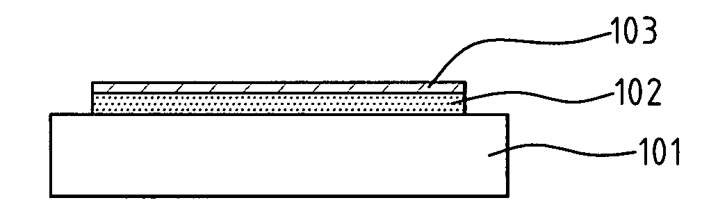
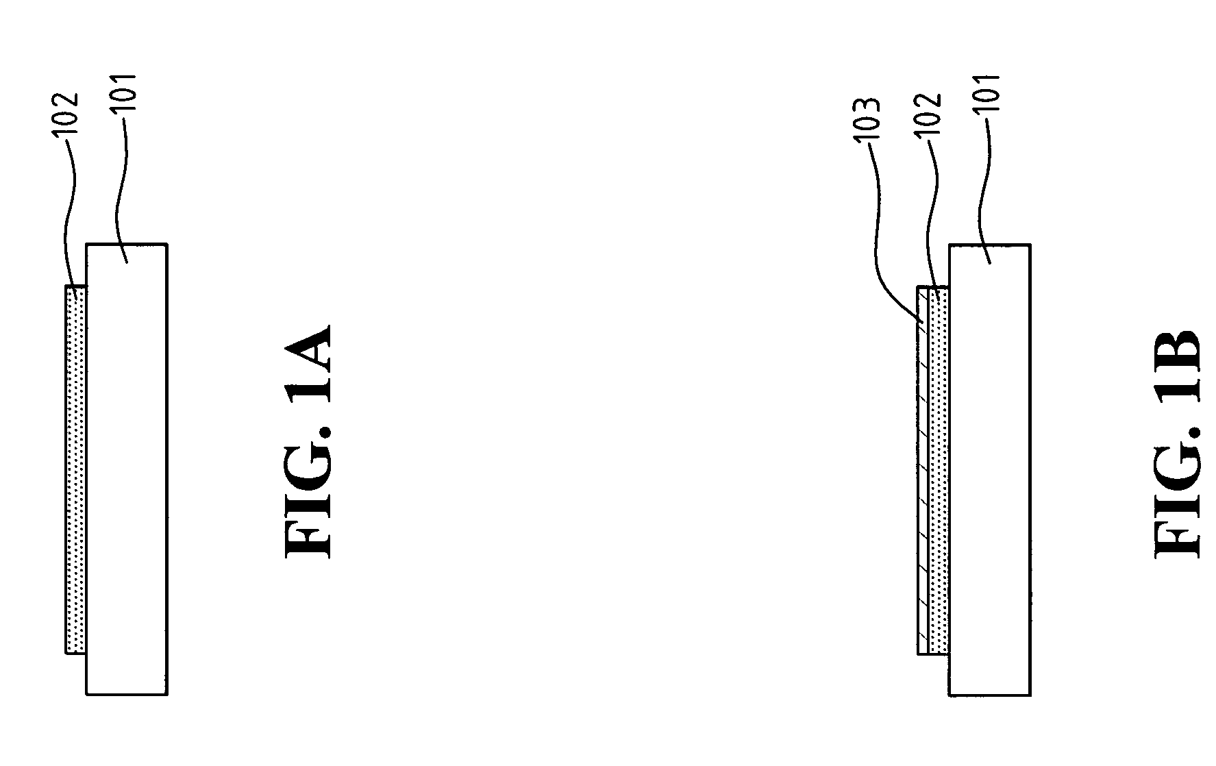
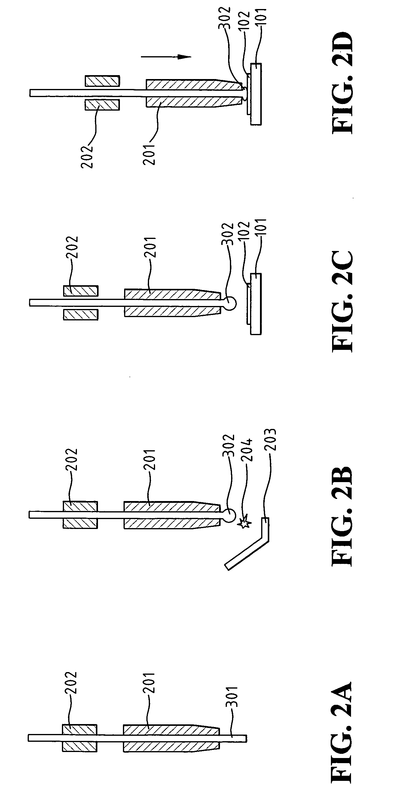
- A thin layer of Cuprous oxide (Cu2O) is formed on the copper bonding-pad using an aqueous solution with controlled pH, which prevents further oxidation and can be easily removed by ultrasonic power to facilitate better bonding.

Copper paste for pressure bonding, semiconductor device, method for preparing copper paste for pressure bonding, and method for manufacturing semiconductor device
PatentWO2023189120A1
Innovation
- A copper paste for pressure bonding is developed, comprising two or more types of copper powders with different shapes and particle sizes, along with a solvent, where the viscosity is adjusted to 10 Pa·s to 200 Pa·s, and the bulkiness index is maintained between 0.75 and 1.00, incorporating spherical and non-spherical copper particles to enhance sinterability and prevent cracking.


Thermal Management Considerations in Copper Clip Design
Thermal management represents a critical design consideration in copper clip bonding applications for thin substrates, as the thermal characteristics directly influence both bonding reliability and long-term performance. The inherent thermal properties of copper clips, combined with the limited thermal mass of thin substrates, create unique challenges that must be addressed through careful design optimization.
The coefficient of thermal expansion (CTE) mismatch between copper clips and thin substrate materials poses significant reliability concerns. Copper exhibits a CTE of approximately 17 ppm/°C, while common thin substrate materials such as silicon or ceramic substrates typically have CTEs ranging from 3-7 ppm/°C. This substantial difference generates thermal stress during temperature cycling, potentially leading to bond line fatigue, delamination, or mechanical failure at the interface.
Heat dissipation efficiency becomes particularly challenging in thin substrate applications due to reduced thermal pathways. The limited substrate thickness restricts vertical heat conduction, making lateral heat spreading through the copper clip increasingly important. Design considerations must account for optimized clip geometry to maximize thermal spreading while maintaining mechanical integrity during bonding processes.
Thermal interface resistance at the copper clip-substrate junction significantly impacts overall thermal performance. Surface roughness, bonding pressure, and intermediate layer materials all contribute to thermal resistance. Advanced surface treatments and optimized bonding parameters are essential to minimize thermal interface resistance and ensure effective heat transfer from the active device through the copper clip to the substrate.
Temperature gradients during bonding processes require careful control to prevent warpage and stress concentration in thin substrates. The rapid heating and cooling cycles typical in copper clip bonding can induce non-uniform thermal expansion, leading to substrate bowing or cracking. Thermal management strategies must incorporate controlled heating profiles and potentially preheating techniques to minimize thermal shock.
Design optimization for thermal management involves balancing clip thickness, surface area, and geometric features to achieve optimal thermal performance while maintaining bondability. Finite element thermal modeling becomes essential for predicting temperature distributions and identifying potential hot spots or thermal bottlenecks in the overall assembly design.
The coefficient of thermal expansion (CTE) mismatch between copper clips and thin substrate materials poses significant reliability concerns. Copper exhibits a CTE of approximately 17 ppm/°C, while common thin substrate materials such as silicon or ceramic substrates typically have CTEs ranging from 3-7 ppm/°C. This substantial difference generates thermal stress during temperature cycling, potentially leading to bond line fatigue, delamination, or mechanical failure at the interface.
Heat dissipation efficiency becomes particularly challenging in thin substrate applications due to reduced thermal pathways. The limited substrate thickness restricts vertical heat conduction, making lateral heat spreading through the copper clip increasingly important. Design considerations must account for optimized clip geometry to maximize thermal spreading while maintaining mechanical integrity during bonding processes.
Thermal interface resistance at the copper clip-substrate junction significantly impacts overall thermal performance. Surface roughness, bonding pressure, and intermediate layer materials all contribute to thermal resistance. Advanced surface treatments and optimized bonding parameters are essential to minimize thermal interface resistance and ensure effective heat transfer from the active device through the copper clip to the substrate.
Temperature gradients during bonding processes require careful control to prevent warpage and stress concentration in thin substrates. The rapid heating and cooling cycles typical in copper clip bonding can induce non-uniform thermal expansion, leading to substrate bowing or cracking. Thermal management strategies must incorporate controlled heating profiles and potentially preheating techniques to minimize thermal shock.
Design optimization for thermal management involves balancing clip thickness, surface area, and geometric features to achieve optimal thermal performance while maintaining bondability. Finite element thermal modeling becomes essential for predicting temperature distributions and identifying potential hot spots or thermal bottlenecks in the overall assembly design.
Reliability Testing Standards for Copper Clip Assemblies
The reliability testing standards for copper clip assemblies in thin substrate applications have evolved significantly to address the unique challenges posed by miniaturized electronic packages. Current industry standards primarily follow JEDEC guidelines, including JESD22-A104 for temperature cycling, JESD22-A108 for highly accelerated stress testing, and JESD22-B117 for salt spray corrosion testing. These standards have been adapted to accommodate the specific failure modes observed in copper clip bonding applications.
Temperature cycling tests typically range from -65°C to 150°C with varying ramp rates and dwell times, specifically designed to evaluate thermal expansion mismatch between copper clips and thin substrates. The standard test duration extends to 1000 cycles minimum, with failure criteria defined by electrical resistance increases exceeding 20% of initial values or visual delamination detection through scanning acoustic microscopy.
Mechanical stress testing protocols incorporate bond shear strength measurements following ASTM D4501 standards, with modifications for copper clip geometries. Pull tests are conducted at controlled rates of 50-100 μm/second, while die shear tests evaluate lateral bond integrity under forces ranging from 5N to 50N depending on clip dimensions. These mechanical evaluations are particularly critical for thin substrates where substrate cracking represents a primary failure mode.
Thermal shock testing employs liquid-to-liquid transfer methods between temperature extremes, typically spanning 200°C differential ranges. This accelerated testing approach effectively identifies weak bonding interfaces and predicts long-term reliability under rapid thermal transients common in power electronics applications.
Environmental stress screening includes humidity resistance testing at 85°C/85% relative humidity for extended periods up to 1000 hours, combined with bias voltage application to simulate operational conditions. Salt spray exposure testing follows modified automotive standards with extended exposure durations to evaluate corrosion resistance of copper metallization systems.
Advanced characterization techniques supplement traditional testing methods, including cross-sectional analysis using focused ion beam preparation and transmission electron microscopy for interface evaluation. These analytical approaches provide detailed failure mechanism identification essential for process optimization and reliability prediction modeling.
Temperature cycling tests typically range from -65°C to 150°C with varying ramp rates and dwell times, specifically designed to evaluate thermal expansion mismatch between copper clips and thin substrates. The standard test duration extends to 1000 cycles minimum, with failure criteria defined by electrical resistance increases exceeding 20% of initial values or visual delamination detection through scanning acoustic microscopy.
Mechanical stress testing protocols incorporate bond shear strength measurements following ASTM D4501 standards, with modifications for copper clip geometries. Pull tests are conducted at controlled rates of 50-100 μm/second, while die shear tests evaluate lateral bond integrity under forces ranging from 5N to 50N depending on clip dimensions. These mechanical evaluations are particularly critical for thin substrates where substrate cracking represents a primary failure mode.
Thermal shock testing employs liquid-to-liquid transfer methods between temperature extremes, typically spanning 200°C differential ranges. This accelerated testing approach effectively identifies weak bonding interfaces and predicts long-term reliability under rapid thermal transients common in power electronics applications.
Environmental stress screening includes humidity resistance testing at 85°C/85% relative humidity for extended periods up to 1000 hours, combined with bias voltage application to simulate operational conditions. Salt spray exposure testing follows modified automotive standards with extended exposure durations to evaluate corrosion resistance of copper metallization systems.
Advanced characterization techniques supplement traditional testing methods, including cross-sectional analysis using focused ion beam preparation and transmission electron microscopy for interface evaluation. These analytical approaches provide detailed failure mechanism identification essential for process optimization and reliability prediction modeling.
Unlock deeper insights with PatSnap Eureka Quick Research — get a full tech report to explore trends and direct your research. Try now!
Generate Your Research Report Instantly with AI Agent
Supercharge your innovation with PatSnap Eureka AI Agent Platform!