Incorporating Green Protocols in Waveguide Grating Production
APR 14, 20269 MIN READ
Generate Your Research Report Instantly with AI Agent
PatSnap Eureka helps you evaluate technical feasibility & market potential.
Green Waveguide Grating Tech Background and Goals
Waveguide gratings have emerged as fundamental components in modern photonic systems, serving critical roles in optical communications, sensing applications, and integrated photonic circuits. These structures, which manipulate light propagation through periodic variations in refractive index or physical geometry, have traditionally been manufactured using processes that prioritize performance over environmental considerations. The conventional production methods often involve energy-intensive fabrication techniques, hazardous chemical etching processes, and materials with significant environmental footprints.
The evolution of waveguide grating technology has progressed through several distinct phases, beginning with early fiber Bragg gratings in the 1970s and advancing to sophisticated integrated photonic structures. Traditional manufacturing approaches have relied heavily on electron beam lithography, reactive ion etching, and chemical vapor deposition processes that consume substantial energy and generate toxic byproducts. These methods, while achieving excellent optical performance, present increasing sustainability challenges as the photonics industry scales to meet growing global demand.
Current environmental pressures and regulatory frameworks are driving a fundamental shift toward sustainable manufacturing practices across the semiconductor and photonics industries. The European Green Deal, various carbon neutrality commitments, and increasing corporate environmental responsibility mandates are creating urgent needs for cleaner production technologies. This transition is particularly critical in waveguide grating manufacturing, where the precision requirements have historically justified environmentally intensive processes.
The primary objective of incorporating green protocols in waveguide grating production centers on developing manufacturing methodologies that maintain or enhance optical performance while dramatically reducing environmental impact. This encompasses minimizing energy consumption during fabrication, eliminating or substituting hazardous chemicals, reducing material waste, and implementing circular economy principles throughout the production lifecycle.
Specific technical goals include achieving comparable grating uniformity and spectral characteristics using low-temperature processing techniques, developing water-based or biodegradable alternatives to traditional photoresists and etchants, and establishing closed-loop manufacturing systems that minimize waste generation. Additionally, the integration of renewable energy sources into fabrication facilities and the development of recyclable substrate materials represent crucial sustainability targets.
The convergence of environmental necessity and technological advancement presents unprecedented opportunities to revolutionize waveguide grating manufacturing. Success in this domain will establish new industry standards while potentially reducing production costs through improved resource efficiency and waste minimization strategies.
Market Demand for Sustainable Photonic Components
The global photonic components market is experiencing unprecedented growth driven by increasing environmental consciousness and regulatory pressures across multiple industries. Telecommunications infrastructure providers are actively seeking sustainable alternatives to traditional manufacturing processes as they expand 5G networks and fiber-optic systems worldwide. This shift represents a fundamental change in procurement strategies, where environmental impact assessments now carry equal weight with performance specifications.
Data center operators constitute another major demand driver, as these facilities consume substantial energy resources and face mounting pressure to achieve carbon neutrality goals. Major cloud service providers have established comprehensive sustainability mandates that extend throughout their supply chains, creating ripple effects that directly impact photonic component manufacturers. The integration of green protocols in waveguide grating production aligns perfectly with these corporate environmental initiatives.
Automotive and aerospace sectors are emerging as significant growth areas for sustainable photonic components, particularly in LiDAR systems and optical sensing applications. Electric vehicle manufacturers prioritize suppliers who demonstrate measurable environmental improvements in their production processes. Similarly, aerospace companies are incorporating sustainability metrics into their vendor qualification processes, recognizing that environmental responsibility enhances brand value and regulatory compliance.
The renewable energy sector presents substantial opportunities for sustainable photonic components, especially in solar panel efficiency optimization and smart grid applications. Wind energy systems increasingly rely on optical sensors for performance monitoring, creating demand for environmentally responsible manufacturing approaches. These applications require long-term reliability while maintaining minimal environmental footprint throughout the product lifecycle.
Government initiatives and regulatory frameworks are accelerating market adoption of sustainable photonic technologies. European Union directives on electronic waste reduction and carbon footprint disclosure are establishing new industry standards that favor green manufacturing protocols. Similar regulatory trends are emerging in North America and Asia-Pacific regions, creating global momentum for sustainable production methods.
Research institutions and universities are driving innovation demand through funded projects focused on environmental sustainability in photonics manufacturing. These academic partnerships often serve as testing grounds for new green protocols before commercial implementation. The collaboration between industry and academia is fostering rapid development of environmentally conscious production techniques that maintain or exceed traditional performance standards.
Current State and Environmental Challenges in Grating Production
The current waveguide grating production industry faces significant environmental challenges that stem from traditional manufacturing processes developed decades ago without sustainability considerations. Conventional fabrication methods rely heavily on energy-intensive lithographic processes, chemical etching techniques, and material deposition systems that generate substantial carbon footprints and hazardous waste streams.
Electron beam lithography and photolithography, the dominant patterning techniques for high-precision gratings, consume enormous amounts of electrical energy while requiring cleanroom environments with continuous air filtration and temperature control. These facilities typically operate 24/7, contributing to substantial energy consumption that often relies on non-renewable power sources. Additionally, the resist materials and developers used in these processes contain volatile organic compounds and toxic solvents that require specialized disposal methods.
Chemical vapor deposition and physical vapor deposition processes used for creating grating structures involve high-temperature operations and reactive gases that pose environmental risks. The production of silicon-based substrates and III-V semiconductor materials requires mining operations and energy-intensive purification processes that contribute to ecological disruption and greenhouse gas emissions.
Waste management represents another critical challenge, as the industry generates significant quantities of contaminated materials including used photoresists, cleaning solvents, and defective substrates. Current disposal methods often involve incineration or landfill storage, neither of which aligns with circular economy principles. The semiconductor fabrication facilities supporting grating production also consume vast quantities of ultrapure water for cleaning processes, straining local water resources.
Supply chain sustainability issues compound these environmental challenges. The global distribution of raw materials, specialized equipment, and finished products creates extensive transportation-related emissions. Many critical materials originate from regions with limited environmental regulations, raising concerns about the overall lifecycle impact of waveguide grating products.
Recent regulatory pressures and corporate sustainability commitments have intensified focus on these environmental impacts. The European Union's Green Deal and similar initiatives worldwide are driving demand for cleaner production methods, while customers increasingly prioritize suppliers with demonstrated environmental responsibility. This regulatory landscape creates both challenges and opportunities for companies willing to invest in sustainable manufacturing approaches.
Existing Green Protocols for Optical Component Production
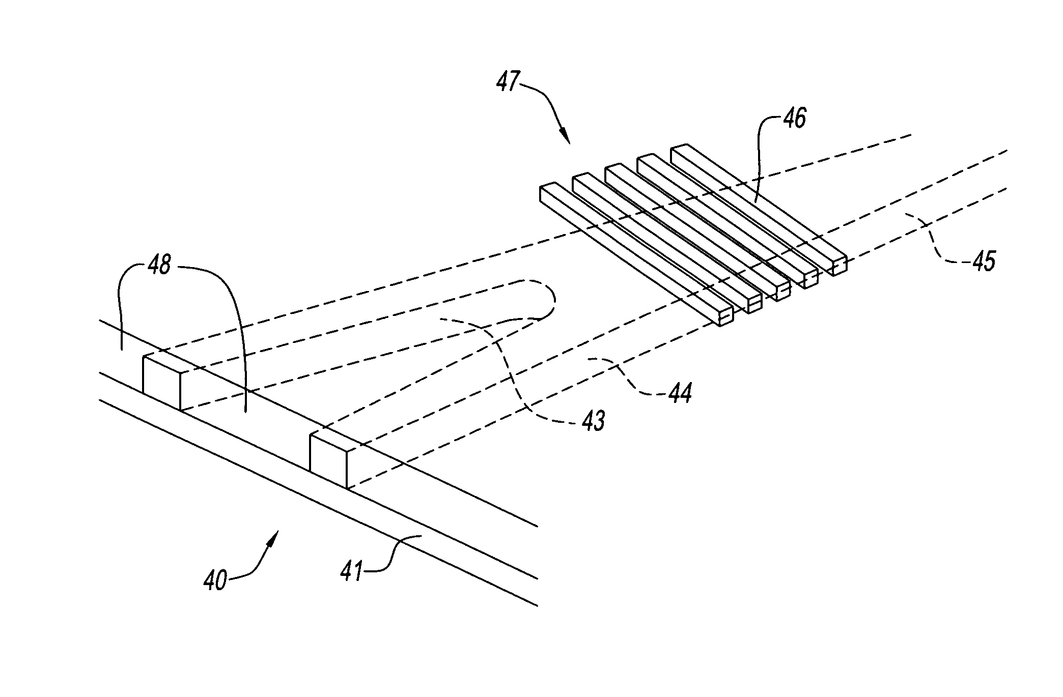
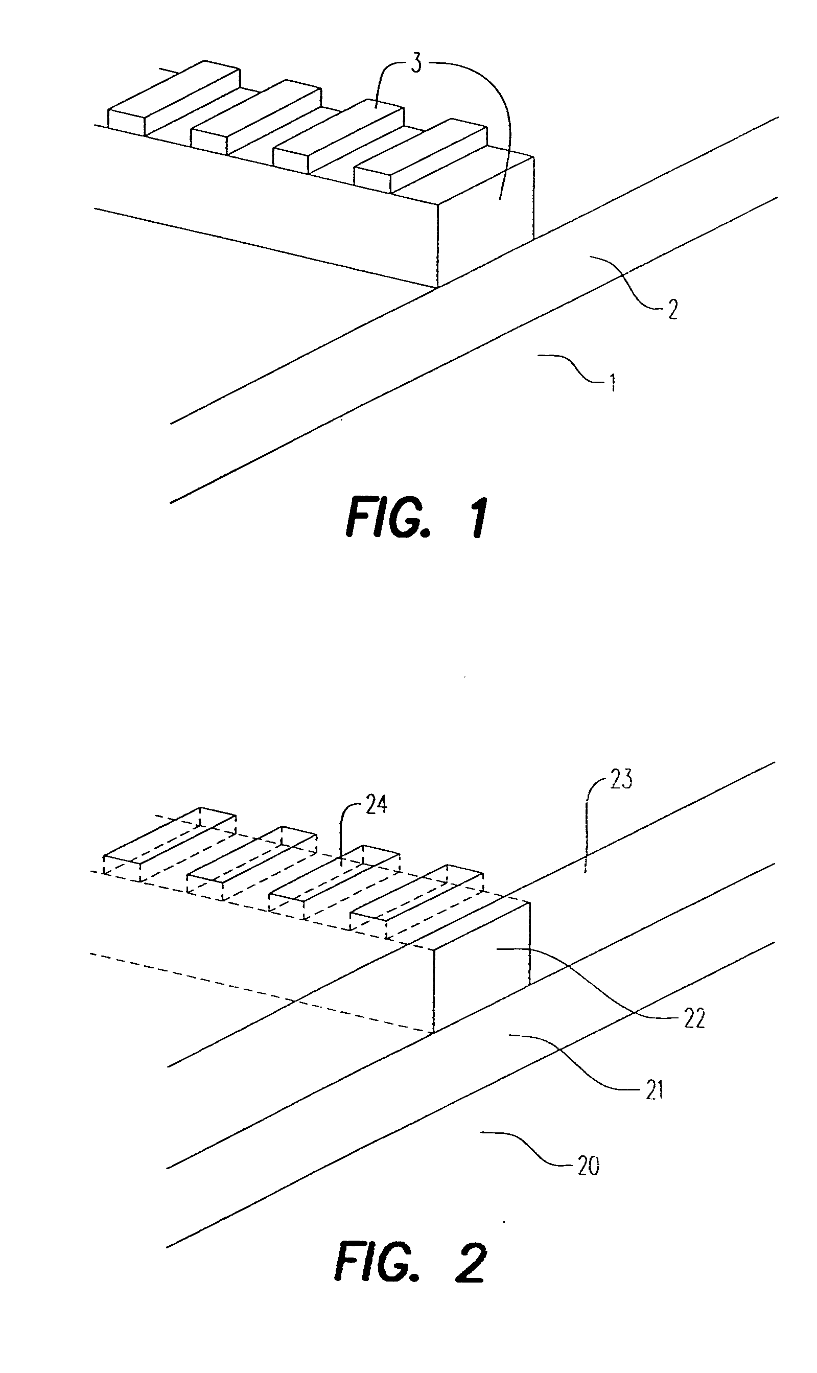
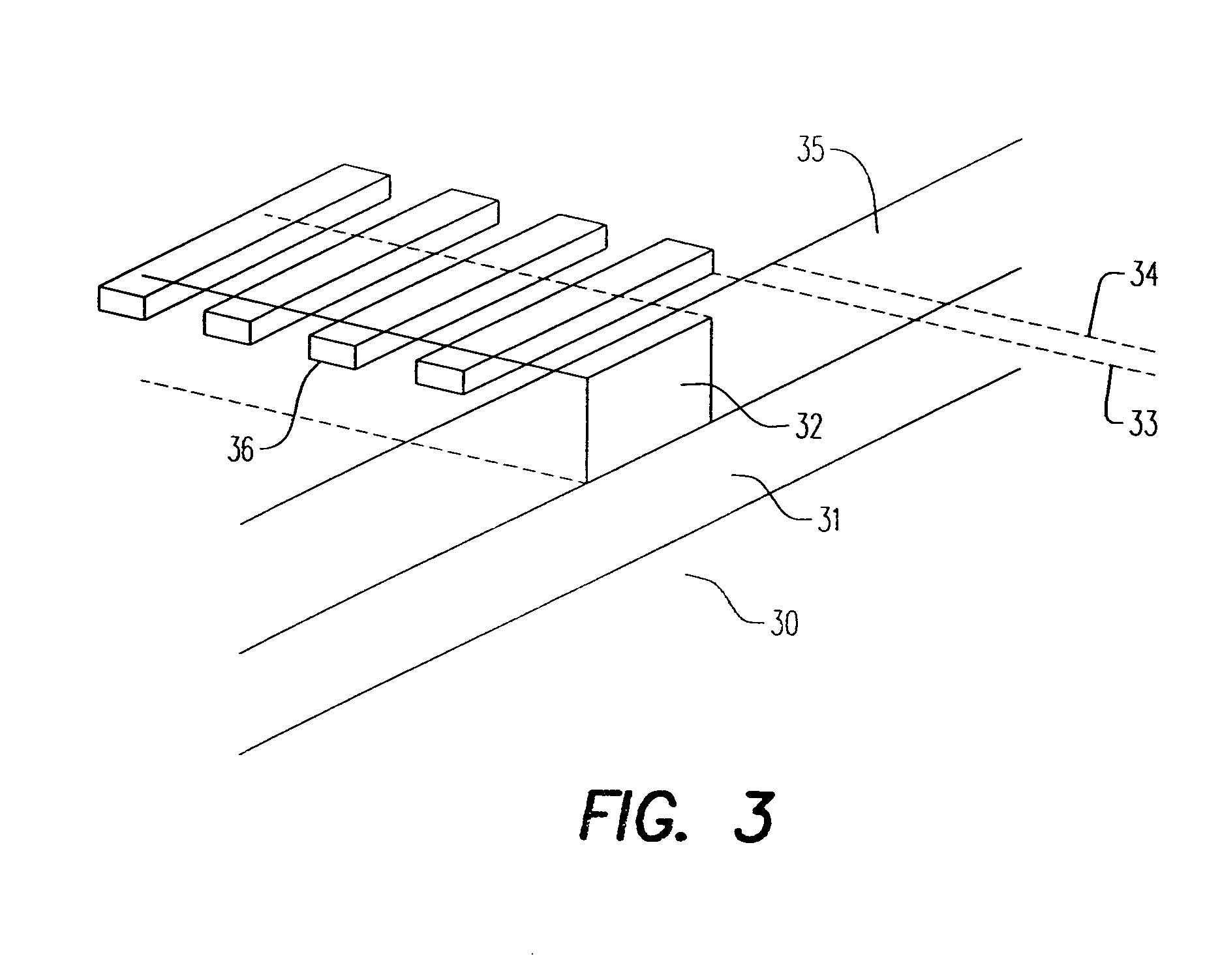
01 Waveguide grating structures for optical coupling and light manipulation
Waveguide gratings are designed with specific structural configurations to efficiently couple light into and out of waveguides. These structures utilize periodic patterns or refractive index modulations to control light propagation, diffraction, and mode conversion. The grating parameters such as period, depth, and duty cycle are optimized to achieve desired optical performance including coupling efficiency and wavelength selectivity.- Waveguide grating structures for optical coupling and light manipulation: Waveguide gratings are designed with specific structural configurations to efficiently couple light into and out of waveguides. These structures utilize periodic patterns or refractive index modulations to control light propagation, diffraction, and mode conversion. The grating parameters such as period, depth, and duty cycle are optimized to achieve desired optical performance including coupling efficiency and wavelength selectivity.
- Diffractive waveguide gratings for display applications: Waveguide gratings are employed in display systems, particularly for augmented reality and virtual reality devices. These gratings enable in-coupling, pupil expansion, and out-coupling of image light within thin waveguide substrates. The grating designs facilitate wide field of view, uniform brightness distribution, and compact form factors for head-mounted displays and near-eye optical systems.
- Blazed and slanted grating configurations for enhanced diffraction efficiency: Specialized grating geometries including blazed profiles and slanted structures are utilized to improve diffraction efficiency in specific orders and directions. These configurations optimize the angular distribution of diffracted light and minimize unwanted reflections. The asymmetric grating profiles enable preferential coupling of light in desired propagation modes while suppressing losses.
- Fabrication methods for waveguide gratings including holographic and lithographic techniques: Various manufacturing approaches are employed to create waveguide gratings with precise dimensional control. Techniques include holographic recording, photolithography, electron beam lithography, and nanoimprint methods. These fabrication processes enable the production of gratings with submicron features, high uniformity, and reproducibility for both surface relief and volume grating structures.
- Wavelength-selective and multiplexed waveguide gratings: Waveguide gratings are designed to provide wavelength-dependent optical functions including filtering, demultiplexing, and spectral separation. Multiple grating structures can be integrated or overlapped within a single waveguide to handle different wavelength channels simultaneously. These configurations enable applications in optical communications, sensing, and multi-color display systems with independent control of different spectral components.
02 Diffractive waveguide gratings for display applications
Waveguide gratings are employed in display systems, particularly for augmented reality and virtual reality devices. These gratings enable in-coupling, propagation, and out-coupling of image light within thin waveguide substrates. The grating designs facilitate pupil expansion and field of view enhancement while maintaining compact form factors. Multiple grating regions with different characteristics can be integrated to achieve full-color display capabilities.Expand Specific Solutions03 Blazed and slanted grating configurations for enhanced efficiency
Specialized grating geometries including blazed profiles and slanted structures are utilized to improve diffraction efficiency and directional light control. These configurations optimize the angular distribution of diffracted light and minimize unwanted diffraction orders. The asymmetric grating profiles enable preferential coupling in specific directions, which is particularly beneficial for applications requiring high efficiency in a particular diffraction order.Expand Specific Solutions04 Fabrication methods for waveguide gratings including holographic and lithographic techniques
Various manufacturing approaches are employed to create waveguide gratings with precise dimensional control. Holographic recording techniques use interference patterns to form grating structures in photosensitive materials. Lithographic methods including electron beam and photolithography combined with etching processes enable high-resolution grating fabrication. Replication techniques such as nanoimprinting allow cost-effective mass production of grating structures with maintained fidelity.Expand Specific Solutions05 Multilayer and volume grating architectures for wavelength selectivity
Advanced waveguide grating designs incorporate multilayer structures or volume gratings to achieve wavelength-selective optical properties. These architectures utilize Bragg reflection principles and distributed feedback mechanisms to provide narrow-band filtering and wavelength-dependent routing. The three-dimensional grating structures enable simultaneous control of multiple wavelengths and polarization states, making them suitable for wavelength division multiplexing and spectroscopic applications.Expand Specific Solutions
Key Players in Sustainable Waveguide Manufacturing
The waveguide grating production industry is experiencing a transformative phase as green protocols become increasingly critical for sustainable manufacturing. The market is in an early-to-mature development stage, driven by growing environmental regulations and corporate sustainability commitments. Market size is expanding rapidly, particularly in AR/VR applications and telecommunications, with significant growth potential in automotive and aerospace sectors. Technology maturity varies considerably across the competitive landscape. Industry leaders like Applied Materials, Taiwan Semiconductor Manufacturing, and DuPont demonstrate advanced green manufacturing capabilities through established sustainable production processes. Technology innovators including DigiLens, Magic Leap, and Snap are integrating environmental considerations into next-generation waveguide designs. Research institutions such as Huazhong University of Science & Technology, Tianjin University, and Fraunhofer-Gesellschaft are developing breakthrough eco-friendly fabrication methods. Emerging players like SVG Group and specialized optoelectronics companies are focusing on energy-efficient manufacturing techniques, while established semiconductor manufacturers are adapting existing green protocols to waveguide production requirements.
Applied Materials, Inc.
Technical Solution: Applied Materials has developed advanced green manufacturing protocols for waveguide grating production through their precision etching and deposition systems. Their approach incorporates low-temperature plasma processing techniques that reduce energy consumption by up to 40% compared to traditional thermal processes. The company utilizes environmentally friendly precursor gases and implements closed-loop chemical recycling systems to minimize waste generation. Their atomic layer deposition (ALD) and plasma-enhanced chemical vapor deposition (PECVD) systems are optimized for precise waveguide grating fabrication while maintaining strict environmental compliance standards.
Strengths: Industry-leading equipment technology, established green manufacturing expertise, comprehensive waste reduction systems. Weaknesses: High initial capital investment, complex system integration requirements.
Taiwan Semiconductor Manufacturing Co., Ltd.
Technical Solution: TSMC has implemented comprehensive green protocols in their advanced packaging and photonic device manufacturing, including waveguide gratings. Their approach focuses on water-based photoresist systems and solvent-free cleaning processes that eliminate hazardous chemical usage by over 60%. The company employs advanced lithography techniques with reduced exposure times and optimized mask designs to minimize material waste. Their green manufacturing framework includes energy-efficient cleanroom operations, waste heat recovery systems, and closed-loop water recycling that achieves 95% water reuse efficiency in waveguide fabrication processes.
Strengths: Advanced semiconductor manufacturing expertise, proven green technology implementation, high-volume production capabilities. Weaknesses: Limited focus on specialized photonic applications, high complexity in process adaptation.
Core Innovations in Eco-Friendly Grating Fabrication
Optical waveguides and grating structures fabricated using polymeric dielectric compositions
PatentInactiveUS6985663B2
Innovation
- A method using polymeric dielectric materials, such as bisbenzocyclobutene (BCB), combined with electron beam lithography for patterning, allowing for precise fabrication of optical waveguides and gratings with dimensions between 5 nm and 50 nm, enabling the creation of complex integrated devices like tunable optical filters and photonic crystals.

Optical waveguide grating and production method therefor
PatentInactiveEP0800098B1
Innovation
- Incorporating boron-doped silica glass with germanium in the core of the optical fiber gratings, where the boron concentration is less than or equal to twice the germanium concentration, to balance refractive index changes with temperature, thereby reducing the temperature dependence of the central wavelength.


Environmental Regulations for Photonic Device Manufacturing
The photonic device manufacturing industry faces increasingly stringent environmental regulations that directly impact waveguide grating production processes. The European Union's RoHS Directive restricts the use of hazardous substances including lead, mercury, cadmium, and hexavalent chromium in electronic and photonic components. Similarly, the WEEE Directive mandates proper disposal and recycling protocols for end-of-life photonic devices, requiring manufacturers to establish take-back programs and achieve specific recycling targets.
In the United States, the EPA's Toxic Substances Control Act governs the use of chemical substances in manufacturing processes, while OSHA regulations establish workplace safety standards for handling potentially hazardous materials used in waveguide fabrication. The Clean Air Act imposes emission limits on volatile organic compounds and particulate matter generated during etching and deposition processes commonly employed in grating production.
Regional regulations vary significantly across manufacturing hubs. China's National Standards for Electronic Information Products mandate compliance with substance restrictions similar to RoHS, while Japan's Green Procurement guidelines encourage the adoption of environmentally friendly materials and processes. These regulations create compliance challenges for global manufacturers who must navigate multiple regulatory frameworks simultaneously.
Emerging regulations focus on carbon footprint reduction and energy efficiency requirements. The EU's Green Deal initiatives are driving new standards for manufacturing energy consumption and greenhouse gas emissions. Several jurisdictions are implementing extended producer responsibility frameworks that hold manufacturers accountable for the entire lifecycle environmental impact of their photonic devices.
Compliance monitoring mechanisms include mandatory environmental impact assessments, regular auditing requirements, and certification processes through recognized standards bodies. Non-compliance penalties range from production shutdowns to substantial financial penalties, making regulatory adherence a critical business imperative. The regulatory landscape continues evolving toward more comprehensive sustainability requirements, necessitating proactive adaptation of manufacturing processes and supply chain management practices in waveguide grating production facilities.
Carbon Footprint Assessment in Waveguide Production
Carbon footprint assessment in waveguide grating production represents a critical evaluation framework for quantifying greenhouse gas emissions throughout the manufacturing lifecycle. This assessment encompasses direct emissions from energy consumption during fabrication processes, indirect emissions from electricity usage, and embedded carbon in raw materials such as silicon substrates, photoresist chemicals, and metallic coatings. The evaluation methodology typically follows ISO 14067 standards, measuring emissions in CO2 equivalents per unit of produced waveguide gratings.
The manufacturing phase contributes the most significant portion of carbon emissions, particularly during high-temperature processes like thermal oxidation, annealing, and chemical vapor deposition. Electron beam lithography and plasma etching processes also generate substantial emissions due to their energy-intensive nature and the use of fluorinated gases with high global warming potential. Studies indicate that conventional waveguide grating production generates approximately 15-25 kg CO2eq per square centimeter of active grating area, with energy consumption accounting for 60-70% of total emissions.
Material sourcing represents another substantial carbon contributor, especially for high-purity silicon wafers and specialized optical coatings. Transportation of materials from suppliers to manufacturing facilities adds approximately 5-8% to the overall carbon footprint, while packaging and end-of-life disposal contribute an additional 3-5%. The assessment reveals that cleanroom operations, including air filtration and temperature control systems, constitute nearly 20% of facility-related emissions.
Recent lifecycle assessments demonstrate significant variation in carbon intensity across different production scales and technologies. Smaller-scale research facilities typically exhibit 40-60% higher carbon intensity compared to industrial-scale manufacturing due to economies of scale in energy efficiency. Advanced manufacturing techniques utilizing lower-temperature processes and renewable energy sources have achieved carbon footprint reductions of 30-45% compared to conventional methods.
The assessment framework also considers scope 3 emissions, including supplier activities and downstream processing. Integration of real-time monitoring systems enables continuous carbon tracking throughout production cycles, facilitating immediate identification of emission hotspots and optimization opportunities for implementing targeted green protocols in waveguide grating manufacturing processes.
Unlock deeper insights with PatSnap Eureka Quick Research — get a full tech report to explore trends and direct your research. Try now!
Generate Your Research Report Instantly with AI Agent
Supercharge your innovation with PatSnap Eureka AI Agent Platform!