

Waveguide Gratings in Precision Optics: Improving Alignment
APR 14, 20269 MIN READ
Generate Your Research Report Instantly with AI Agent
PatSnap Eureka helps you evaluate technical feasibility & market potential.
Waveguide Grating Technology Background and Precision Goals
Waveguide gratings represent a fundamental convergence of photonic engineering and precision optics, emerging from decades of advancement in integrated photonics and diffractive optical elements. These structures combine the light-guiding properties of optical waveguides with the wavelength-selective characteristics of diffraction gratings, creating versatile components essential for modern optical systems. The technology traces its origins to early fiber optic communications research in the 1970s, where researchers first explored periodic structures within optical fibers to manipulate light propagation.
The evolution of waveguide grating technology has been driven by the increasing demand for miniaturization and integration in optical systems. Traditional bulk optical components, while effective, present significant challenges in terms of size, weight, and manufacturing complexity. Waveguide gratings address these limitations by enabling on-chip integration of optical functions, facilitating the development of compact, robust, and cost-effective photonic devices.
Current technological trends indicate a strong emphasis on improving fabrication precision and alignment accuracy. Advanced lithographic techniques, including electron beam lithography and deep ultraviolet photolithography, have enabled the creation of gratings with sub-nanometer feature control. These manufacturing improvements directly translate to enhanced optical performance, reduced insertion losses, and improved spectral selectivity.
The precision alignment challenge in waveguide gratings stems from the stringent requirements for optimal coupling efficiency and spectral response. Misalignment tolerances often fall within nanometer ranges, demanding sophisticated positioning systems and real-time feedback mechanisms. This challenge becomes particularly acute in applications requiring wavelength-division multiplexing, where precise spectral channel separation is critical.
Primary technical objectives focus on achieving sub-degree angular alignment accuracy while maintaining high coupling efficiency across broad spectral ranges. Advanced alignment systems now incorporate machine learning algorithms and adaptive optics to compensate for manufacturing variations and environmental fluctuations. These developments aim to establish robust, self-correcting optical systems capable of maintaining optimal performance under varying operational conditions.
The integration of waveguide gratings with emerging technologies such as silicon photonics and quantum optics presents new opportunities for breakthrough applications. Future developments target achieving alignment precision approaching the fundamental limits imposed by quantum mechanical effects, potentially enabling revolutionary advances in optical computing, sensing, and telecommunications infrastructure.
Market Demand for High-Precision Optical Alignment Systems
The global market for high-precision optical alignment systems is experiencing robust growth driven by the increasing sophistication of optical technologies across multiple industries. The demand for waveguide gratings in precision optics applications has intensified as industries require more accurate and reliable optical alignment solutions to meet stringent performance specifications.
Telecommunications infrastructure represents one of the largest market segments, where fiber optic networks demand precise alignment systems to minimize signal loss and maximize data transmission efficiency. The ongoing expansion of 5G networks and the development of next-generation communication systems have created substantial demand for advanced optical alignment technologies that can maintain sub-micron precision levels.
The aerospace and defense sector constitutes another significant market driver, requiring ultra-precise optical systems for satellite communications, laser guidance systems, and advanced imaging applications. These applications demand alignment systems capable of maintaining stability under extreme environmental conditions while delivering exceptional accuracy.
Medical device manufacturing has emerged as a rapidly growing market segment, particularly in laser surgery equipment, optical coherence tomography systems, and precision diagnostic instruments. The increasing adoption of minimally invasive surgical procedures and advanced medical imaging technologies has created substantial demand for high-precision optical alignment solutions.
Industrial manufacturing applications, including laser processing, semiconductor fabrication, and quality control systems, represent a substantial portion of the market demand. The trend toward automation and Industry 4.0 initiatives has accelerated the need for precise optical alignment systems that can integrate seamlessly with automated manufacturing processes.
Research and development institutions, including universities and government laboratories, continue to drive demand for cutting-edge optical alignment systems. These organizations require highly precise and flexible alignment solutions for experimental setups and advanced research applications.
The market exhibits strong regional variations, with North America and Europe leading in terms of technological advancement and adoption rates, while Asia-Pacific regions show the highest growth potential due to expanding manufacturing capabilities and increasing investment in optical technologies.
Market growth is further supported by the increasing complexity of optical systems, which require more sophisticated alignment solutions to achieve optimal performance. The integration of artificial intelligence and machine learning technologies into alignment systems has created new market opportunities and enhanced the value proposition for end users.
Current Waveguide Grating Alignment Challenges and Limitations
Waveguide grating alignment in precision optical systems faces significant challenges stemming from the inherent complexity of coupling light between different optical components with nanometer-scale precision requirements. The fundamental difficulty lies in achieving and maintaining optimal overlap between the optical mode profiles of waveguides and grating structures, which directly impacts coupling efficiency and overall system performance.
Manufacturing tolerances represent a primary constraint in current alignment methodologies. Fabrication processes introduce variations in grating period, duty cycle, and sidewall angles that can deviate from design specifications by several nanometers. These seemingly minor variations translate into substantial alignment sensitivity, requiring compensation mechanisms that often exceed the capabilities of conventional positioning systems.
Thermal stability poses another critical limitation, as temperature fluctuations cause differential expansion between various materials in the optical assembly. Silicon-based waveguides and polymer-based gratings exhibit different thermal expansion coefficients, leading to dynamic misalignment that varies with environmental conditions. This thermal drift necessitates active compensation systems that add complexity and cost to precision optical implementations.
Current alignment techniques predominantly rely on active feedback systems that monitor optical power transmission while adjusting mechanical positioning stages. However, these approaches suffer from limited resolution and speed constraints. Piezoelectric actuators, while offering sub-nanometer positioning accuracy, exhibit hysteresis and creep effects that compromise long-term alignment stability.
The multi-dimensional nature of the alignment problem compounds these difficulties. Optimal coupling requires simultaneous control of lateral position, angular orientation, and gap spacing between waveguide and grating elements. Traditional sequential optimization approaches often result in local minima rather than global alignment optima, particularly when dealing with asymmetric mode profiles or non-uniform grating structures.
Measurement and characterization limitations further constrain alignment precision. Conventional optical power monitoring provides insufficient information about the spatial distribution of coupling efficiency, making it difficult to distinguish between different misalignment modes. Near-field scanning techniques offer higher spatial resolution but require specialized equipment and extended measurement times that are incompatible with high-throughput manufacturing requirements.
Dynamic environmental factors, including vibration, air currents, and electromagnetic interference, introduce additional alignment perturbations that current passive mounting systems cannot adequately suppress. These external influences become increasingly problematic as precision requirements tighten, often necessitating expensive isolation systems that may not be practical for all applications.
Existing Alignment Solutions for Waveguide Gratings
01 Active alignment methods using optical feedback
Active alignment techniques involve monitoring optical signals during the alignment process to achieve precise positioning of waveguide gratings. This method uses real-time feedback from transmitted or reflected light to optimize coupling efficiency. The alignment process typically involves adjusting the position and angle of components while measuring optical performance parameters such as insertion loss or coupling efficiency. This approach enables high-precision alignment by continuously monitoring and adjusting based on optical output.- Optical alignment methods using interference patterns: Waveguide gratings can be aligned using optical interference patterns generated by the gratings themselves. This method involves detecting the interference fringes or diffraction patterns produced when light passes through or reflects from the grating structures. The alignment is achieved by analyzing these patterns and adjusting the position of the waveguide or grating until optimal interference conditions are met. This technique provides high precision alignment without requiring physical contact with the components.
- Active alignment using photodetectors and feedback control: Active alignment techniques employ photodetectors to measure the optical coupling efficiency or output power during the alignment process. A feedback control system continuously monitors the detected signal and adjusts the position of the waveguide grating in multiple degrees of freedom to maximize coupling efficiency. This approach enables real-time optimization and can compensate for manufacturing tolerances and environmental variations. The system typically includes actuators for precise positioning and algorithms for determining optimal alignment positions.
- Mechanical alignment structures and fixtures: Specialized mechanical structures and fixtures are designed to facilitate the alignment of waveguide gratings. These include precision alignment marks, registration features, grooves, or mechanical stops that provide reference points for positioning. The structures may be integrated into the waveguide substrate or grating component itself, or provided as separate alignment fixtures. Such mechanical aids enable passive alignment approaches where components self-align when brought together, reducing the complexity and time required for assembly.
- Vision-based alignment using imaging systems: Vision-based alignment methods utilize imaging systems such as cameras or microscopes to capture images of alignment marks or features on the waveguide and grating components. Image processing algorithms analyze these images to determine the relative positions and orientations of the components. The system calculates the required adjustments and guides the positioning equipment to achieve proper alignment. This approach is particularly useful for aligning arrays of waveguide gratings or when visual inspection of alignment features is feasible.
- Multi-axis positioning and angular alignment control: Precise alignment of waveguide gratings requires control over multiple axes including translational movements in three dimensions and rotational adjustments for angular orientation. Specialized positioning systems with multiple degrees of freedom enable fine adjustments to optimize coupling efficiency and minimize losses. These systems may incorporate piezoelectric actuators, stepper motors, or other precision motion control devices. Angular alignment is particularly critical for grating-based devices where the angle of incidence affects the coupling efficiency and wavelength selectivity.
02 Passive alignment using mechanical features and alignment marks
Passive alignment techniques utilize pre-fabricated mechanical features, alignment marks, or reference structures to position waveguide gratings without active optical monitoring. This approach includes the use of alignment grooves, V-grooves, registration marks, or fiducial markers that are integrated into the substrate or component design. The method enables cost-effective and rapid alignment by relying on mechanical precision and visual or automated recognition of alignment features. This technique is particularly suitable for mass production scenarios.Expand Specific Solutions03 Alignment structures and coupling configurations for grating couplers
Specialized structural designs and coupling configurations are employed to facilitate the alignment of waveguide gratings. These include specific grating geometries, tapered waveguide sections, and optimized coupling regions that provide increased alignment tolerance. The designs may incorporate features such as expanded mode field areas, adiabatic tapers, or multi-stage coupling structures that reduce sensitivity to misalignment. Such configurations help maintain acceptable optical performance even with minor positioning errors.Expand Specific Solutions04 Automated alignment systems and vision-based positioning
Automated alignment systems employ machine vision, image processing, and robotic positioning to achieve precise waveguide grating alignment. These systems typically use cameras or optical sensors to detect alignment features and calculate positioning corrections. The automation includes pattern recognition algorithms, edge detection, and coordinate transformation to guide precision stages or actuators. This approach enables repeatable, high-throughput alignment with minimal human intervention and is particularly valuable in manufacturing environments.Expand Specific Solutions05 Multi-axis adjustment mechanisms and fine-tuning methods
Multi-axis adjustment mechanisms provide precise control over multiple degrees of freedom during waveguide grating alignment. These systems incorporate stages or actuators that enable independent adjustment of position, tilt, and rotation in multiple axes. Fine-tuning methods include piezoelectric actuators, micrometers, or MEMS-based positioning devices that offer sub-micron resolution. The combination of coarse and fine adjustment capabilities allows for both initial positioning and final optimization of alignment to achieve maximum coupling efficiency.Expand Specific Solutions
Key Players in Precision Optics and Waveguide Industry
The waveguide gratings in precision optics market is experiencing rapid growth driven by increasing demand for high-precision alignment solutions across semiconductor lithography, AR/VR displays, and optical communications. The industry is in an expansion phase with significant market potential, particularly in Asia-Pacific regions. Technology maturity varies considerably among key players: established leaders like ASML Netherlands BV and Applied Materials demonstrate advanced lithography capabilities, while Shanghai Microelectronics Equipment and Shanghai Weigao Precision Machinery represent emerging Chinese competitors in semiconductor equipment. AR/VR specialists including DigiLens and Dispelex Oy are advancing waveguide display technologies, supported by tech giants Google LLC, Microsoft Technology Licensing LLC, and Intel Corp. The competitive landscape shows a mix of mature semiconductor equipment manufacturers, innovative optics startups, and research institutions like MIT, indicating a dynamic ecosystem with varying technological readiness levels across different application segments.
Dispelix Oy
Technical Solution: Dispelix specializes in waveguide display technologies with advanced grating alignment systems for AR applications. Their proprietary manufacturing process incorporates high-precision alignment techniques using specialized tooling and measurement systems to achieve consistent grating positioning across large-area substrates. The company's waveguide gratings utilize surface relief structures with optimized coupling efficiency, featuring alignment tolerances in the micrometer range while maintaining high optical performance. Their manufacturing approach includes automated alignment verification systems and real-time process monitoring to ensure consistent product quality and optical specifications.
Strengths: Specialized expertise in waveguide manufacturing, proven mass production capabilities, cost-effective solutions for AR applications. Weaknesses: Limited to display applications, smaller scale compared to major tech companies, narrow technology focus.
ASML Netherlands BV
Technical Solution: ASML develops advanced waveguide grating systems for extreme ultraviolet (EUV) lithography applications, utilizing high-precision alignment mechanisms that achieve sub-nanometer positioning accuracy. Their waveguide gratings incorporate sophisticated interferometric feedback systems with real-time correction algorithms to maintain optimal beam coupling efficiency during wafer processing. The company's proprietary grating designs feature specialized surface relief structures optimized for specific wavelengths, enabling precise control of diffraction angles and beam steering capabilities essential for next-generation semiconductor manufacturing processes.
Strengths: Industry-leading precision in nanometer-scale alignment, extensive R&D resources, dominant market position in advanced lithography. Weaknesses: Extremely high costs, complex system integration requirements, limited application scope beyond semiconductor manufacturing.
Core Innovations in Waveguide Grating Alignment Methods
Arrayed waveguide gratings with improved transmission efficiency
PatentInactiveUS6956993B2
Innovation
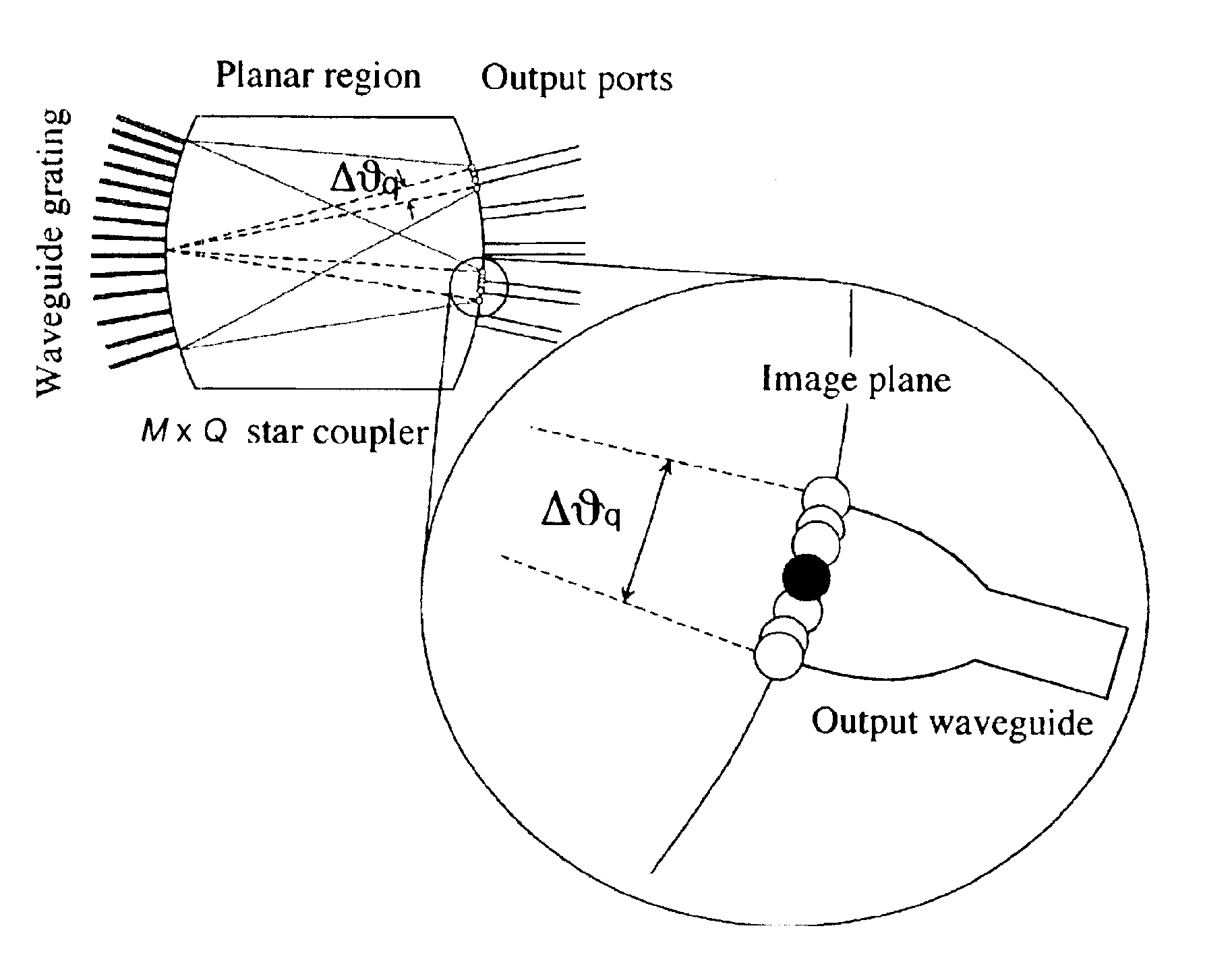
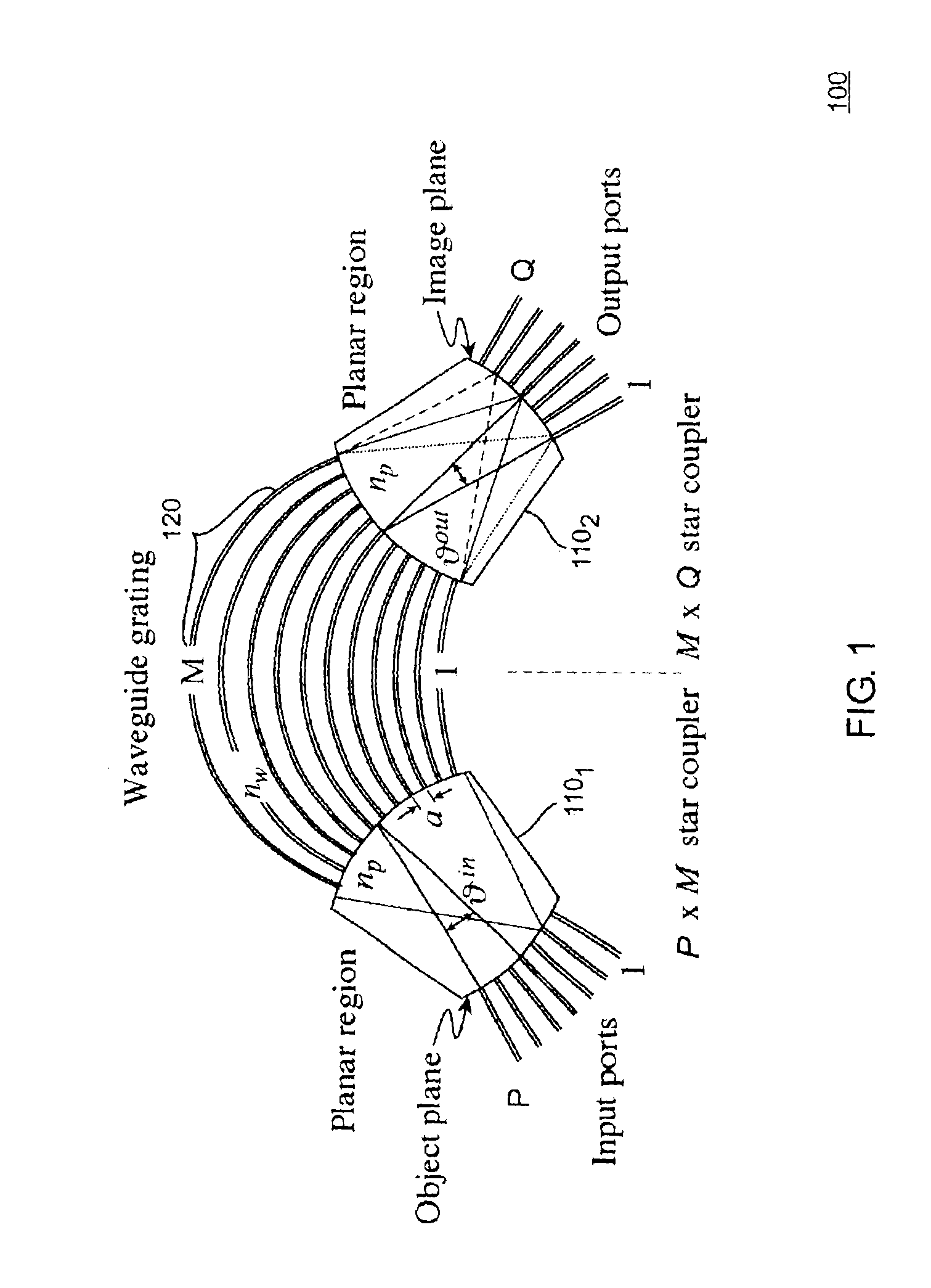
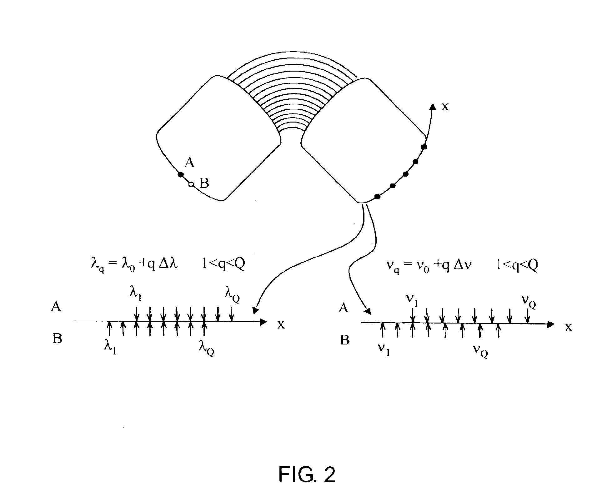
- The method involves optimizing the positioning of input and output ports in arrayed waveguide gratings by determining the initial positions based on wavelength dispersion images and iteratively adjusting them to minimize the maximum angular spread of image combs, allowing for improved alignment and increased transmission efficiency by operating within a single diffraction order and repositioning output ports to maximize signal transmission coefficients.

Reducing amplitude errors in arrayed waveguide gratings
PatentInactiveUS7391941B2
Innovation
- Tuning the input/output waveguides to reduce amplitude aberrations by adjusting their angles to align with a displaced stigmatic point outside the Rowland circle, rather than the conventional center, to balance the power distribution and correct the transmission spectrum asymmetry.


Manufacturing Standards for Precision Optical Components
The manufacturing of precision optical components for waveguide gratings requires adherence to stringent standards that ensure optimal performance in alignment-critical applications. International standards such as ISO 10110 series provide comprehensive guidelines for optical element specifications, including surface quality, dimensional tolerances, and material homogeneity requirements. These standards establish the foundation for manufacturing processes that can achieve the sub-micron precision necessary for effective waveguide grating systems.
Surface roughness specifications represent a critical manufacturing parameter, with typical requirements demanding RMS values below 1 nanometer for grating surfaces. The ISO 10110-8 standard defines acceptable surface imperfection levels, while complementary standards like ANSI/OPTICA OP1.002 provide additional guidance for laser damage threshold specifications. Manufacturing facilities must implement controlled environments with Class 100 or better cleanroom conditions to prevent contamination during fabrication processes.
Dimensional accuracy standards for waveguide gratings typically require tolerances within ±50 nanometers for critical features such as grating period and groove depth. The implementation of coordinate measuring machines (CMMs) with nanometer-level resolution has become essential for quality verification. Manufacturing processes must incorporate real-time monitoring systems that can detect deviations from specified parameters during production cycles.
Material quality standards encompass specifications for optical glass homogeneity, stress birefringence levels, and thermal expansion coefficients. The Schott glass catalog standards and similar industry references define acceptable material properties for precision optical applications. Substrate preparation protocols must ensure surface flatness within λ/20 across the entire component surface, requiring specialized polishing techniques and metrology equipment.
Quality assurance protocols mandate comprehensive testing procedures including interferometric surface analysis, diffraction efficiency measurements, and environmental stability assessments. Traceability requirements necessitate detailed documentation of manufacturing parameters, material certifications, and measurement data throughout the production process. These standards collectively ensure that manufactured components meet the demanding performance requirements of precision waveguide grating systems while maintaining consistency across production batches.
Quality Control in High-Precision Waveguide Systems
Quality control in high-precision waveguide systems represents a critical operational framework that ensures consistent performance and reliability of waveguide grating-based optical devices. The implementation of rigorous quality control protocols becomes particularly essential when addressing alignment challenges in precision optics, where even nanometer-scale deviations can significantly impact system performance.
The foundation of effective quality control lies in establishing comprehensive measurement protocols that can accurately assess waveguide grating alignment parameters. Advanced interferometric techniques, including phase-shifting interferometry and digital holographic microscopy, provide the necessary precision for detecting alignment deviations at the sub-wavelength level. These measurement systems must be calibrated regularly using certified reference standards to maintain traceability and measurement accuracy.
Statistical process control methodologies play a crucial role in maintaining consistent manufacturing quality. Implementation of control charts and capability studies enables real-time monitoring of critical alignment parameters such as grating period uniformity, sidewall angle consistency, and surface roughness variations. These statistical tools help identify process drift before it affects product quality, enabling proactive corrective actions.
Environmental control represents another fundamental aspect of quality assurance in high-precision waveguide systems. Temperature fluctuations, humidity variations, and vibrations can introduce alignment errors during both manufacturing and operation phases. Establishing controlled environments with temperature stability within ±0.1°C and vibration isolation systems becomes essential for maintaining alignment precision.
Automated inspection systems utilizing machine vision and artificial intelligence algorithms enhance quality control efficiency while reducing human error. These systems can perform rapid, non-destructive evaluation of waveguide grating structures, identifying defects such as stitching errors, dose variations, and alignment mismatches that could compromise optical performance.
Documentation and traceability protocols ensure that quality control data is properly recorded and maintained throughout the product lifecycle. This includes maintaining detailed records of measurement results, calibration certificates, and process parameters, enabling root cause analysis when quality issues arise and supporting continuous improvement initiatives in waveguide grating alignment processes.
Unlock deeper insights with PatSnap Eureka Quick Research — get a full tech report to explore trends and direct your research. Try now!
Generate Your Research Report Instantly with AI Agent
Supercharge your innovation with PatSnap Eureka AI Agent Platform!