

Increasing Substrate Yield 2X Using Dedicated FAB Digital Twin Simulations
JUN 3, 20269 MIN READ
Generate Your Research Report Instantly with AI Agent
PatSnap Eureka helps you evaluate technical feasibility & market potential.
Digital Twin FAB Simulation Background and Yield Goals
Digital twin technology has emerged as a transformative approach in semiconductor manufacturing, representing a paradigm shift from traditional process optimization methods. This technology creates virtual replicas of physical fabrication facilities, enabling real-time monitoring, predictive analytics, and process optimization without disrupting actual production lines. The semiconductor industry's increasing complexity, driven by advanced node technologies and stringent quality requirements, has necessitated more sophisticated manufacturing control systems.
The evolution of digital twin applications in semiconductor fabrication began with basic process monitoring systems in the early 2000s, progressing through statistical process control implementations, and advancing to today's comprehensive virtual manufacturing environments. Modern digital twin systems integrate multiple data sources including equipment sensors, environmental monitoring systems, process control databases, and quality inspection results to create holistic manufacturing models.
Current digital twin implementations in semiconductor fabs focus primarily on equipment health monitoring, predictive maintenance, and basic process parameter optimization. However, the potential for yield enhancement through comprehensive substrate-level simulation represents a significant advancement opportunity. Traditional yield improvement methodologies rely heavily on post-production analysis and iterative process adjustments, often requiring multiple production cycles to identify and resolve yield-limiting factors.
The primary objective of implementing dedicated FAB digital twin simulations for substrate yield enhancement centers on achieving a two-fold increase in production yield through predictive modeling and real-time process optimization. This ambitious target requires comprehensive integration of process physics models, statistical analysis algorithms, and machine learning capabilities to predict and prevent yield-limiting events before they occur in actual production.
Key technical goals include developing high-fidelity substrate processing models that accurately simulate chemical mechanical planarization, lithography exposure variations, etching uniformity, and deposition thickness control across entire wafer surfaces. The digital twin system must incorporate real-time data feeds from production equipment to continuously calibrate and refine predictive models, ensuring accuracy and relevance to current manufacturing conditions.
The yield enhancement strategy encompasses multiple operational objectives including reducing defect density through predictive process control, optimizing process parameter combinations for maximum yield potential, minimizing process variation through advanced statistical process control, and enabling rapid identification and correction of yield-limiting equipment conditions. Success metrics include achieving consistent substrate yield improvements of 100% or greater, reducing time-to-detection for yield-limiting events by at least 75%, and decreasing overall manufacturing cycle time through optimized process flows.
Market Demand for Enhanced Semiconductor Yield Solutions
The semiconductor industry faces unprecedented pressure to maximize manufacturing efficiency as device complexity increases and profit margins tighten. Traditional yield optimization approaches have reached their practical limits, creating substantial market demand for revolutionary solutions that can deliver significant performance improvements. The emergence of digital twin technology represents a paradigm shift in how fabrication facilities approach yield enhancement, offering the potential to double substrate yields through advanced simulation capabilities.
Current market dynamics reveal that semiconductor manufacturers are experiencing mounting pressure from multiple directions. Rising material costs, particularly for advanced substrates and rare earth elements, have compressed profit margins across the industry. Simultaneously, the increasing complexity of modern semiconductor devices has made traditional trial-and-error optimization methods both time-consuming and cost-prohibitive. These factors have created an urgent need for predictive technologies that can optimize processes before physical implementation.
The global semiconductor market's rapid expansion has intensified competition among manufacturers to achieve superior yield rates. Companies that can consistently deliver higher yields gain significant competitive advantages through reduced per-unit costs and improved production capacity utilization. This competitive landscape has driven substantial investment in advanced manufacturing technologies, with digital twin solutions emerging as a critical differentiator for leading fabrication facilities.
Manufacturing inefficiencies in semiconductor production result in billions of dollars in annual losses across the industry. Defective substrates, process variations, and equipment downtime contribute to yield losses that directly impact profitability and market competitiveness. The ability to predict and prevent these issues through sophisticated simulation models addresses a fundamental pain point that affects every major semiconductor manufacturer globally.
The convergence of artificial intelligence, machine learning, and high-performance computing has created the technological foundation necessary for effective digital twin implementations. These enabling technologies have matured sufficiently to support real-time simulation of complex fabrication processes, making previously theoretical concepts practically achievable. Market readiness for these solutions has reached a tipping point where the return on investment justifies the substantial implementation costs.
Regulatory pressures and sustainability requirements are adding additional layers of complexity to semiconductor manufacturing. Environmental regulations demand more efficient resource utilization, while quality standards continue to tighten across key market segments. Digital twin solutions that can optimize both yield and resource efficiency address these dual requirements, creating additional market pull for advanced simulation technologies.
Current FAB Yield Challenges and Digital Twin Limitations
Semiconductor fabrication facilities face persistent yield challenges that significantly impact production efficiency and profitability. Traditional yield losses stem from multiple sources including process variations, equipment drift, contamination events, and material defects. These issues compound across the complex multi-step manufacturing process, where hundreds of individual operations must execute flawlessly to produce functional devices.
Process control limitations represent a fundamental challenge in current FAB operations. Existing monitoring systems often rely on post-process measurements and statistical sampling, creating delays between defect occurrence and detection. This reactive approach results in substantial material waste and extended time-to-correction intervals that amplify yield losses across production batches.
Equipment variability introduces another layer of complexity, as identical tools can exhibit subtle performance differences that accumulate over time. Chamber-to-chamber variations, maintenance-induced changes, and aging effects create unpredictable process outcomes that traditional control systems struggle to anticipate or compensate for effectively.
Current digital twin implementations in semiconductor manufacturing face significant technical limitations that restrict their effectiveness for yield optimization. Most existing systems operate with simplified models that cannot capture the full complexity of FAB processes, particularly the intricate interactions between multiple process steps and their cumulative effects on final device performance.
Real-time data integration remains a critical bottleneck for digital twin applications. Many FAB systems generate massive data volumes, but current digital twin platforms lack the computational capacity and algorithmic sophistication to process this information in real-time while maintaining model accuracy and predictive reliability.
Model validation and calibration present ongoing challenges, as digital twins require continuous updates to reflect changing process conditions and equipment states. The complexity of semiconductor processes makes it difficult to establish robust correlations between simulation parameters and actual manufacturing outcomes, limiting the predictive accuracy of current implementations.
Computational resource constraints further limit the scope and resolution of existing digital twin systems. High-fidelity process simulations demand substantial computing power, forcing operators to choose between model accuracy and real-time performance, often resulting in oversimplified representations that miss critical yield-impacting phenomena.
Existing Digital Twin Solutions for Substrate Yield Enhancement
01 Digital twin modeling for semiconductor fabrication processes
Implementation of digital twin technology to create virtual representations of semiconductor fabrication processes, enabling real-time monitoring and optimization of manufacturing parameters. These systems utilize advanced computational models to simulate the entire fabrication workflow, allowing for predictive analysis and process control improvements.- Digital twin modeling and simulation frameworks for semiconductor fabrication: Advanced digital twin technologies that create virtual representations of semiconductor fabrication processes to enable real-time monitoring, prediction, and optimization of manufacturing operations. These frameworks integrate multiple data sources and use sophisticated algorithms to mirror physical fab operations digitally.
- Substrate yield optimization through predictive analytics: Machine learning and artificial intelligence approaches that analyze historical production data, process parameters, and environmental conditions to predict and optimize substrate yield rates. These methods identify patterns and correlations that help prevent defects and improve overall manufacturing efficiency.
- Real-time process monitoring and control systems: Integrated monitoring solutions that continuously track fabrication processes and automatically adjust parameters to maintain optimal substrate yield. These systems use sensors, data analytics, and feedback loops to detect anomalies and implement corrective actions in real-time during production.
- Quality control and defect prediction methodologies: Comprehensive quality assurance frameworks that employ advanced inspection techniques, statistical analysis, and predictive modeling to identify potential defects before they impact substrate yield. These methodologies focus on early detection and prevention of manufacturing issues.
- Data integration and analytics platforms for fab operations: Centralized data management and analytics platforms that collect, process, and analyze information from various fabrication equipment and processes. These platforms provide insights into production efficiency, equipment performance, and yield optimization opportunities through comprehensive data visualization and reporting tools.
02 Substrate yield optimization through simulation algorithms
Development of sophisticated simulation algorithms specifically designed to maximize substrate yield in semiconductor manufacturing. These algorithms analyze various process parameters and material properties to identify optimal conditions that minimize defects and waste while maximizing production efficiency.Expand Specific Solutions03 Machine learning integration for predictive yield analysis
Integration of machine learning and artificial intelligence techniques into fabrication simulation systems to predict substrate yield outcomes. These systems learn from historical production data and real-time process measurements to forecast potential yield issues and recommend corrective actions before defects occur.Expand Specific Solutions04 Real-time process monitoring and control systems
Implementation of advanced monitoring and control systems that provide real-time feedback on fabrication processes to maintain optimal substrate yield. These systems continuously track critical process variables and automatically adjust parameters to ensure consistent quality and maximize production output.Expand Specific Solutions05 Multi-parameter optimization for fabrication efficiency
Development of comprehensive optimization frameworks that simultaneously consider multiple fabrication parameters to achieve maximum substrate yield. These systems balance various competing factors such as processing time, material usage, energy consumption, and quality requirements to determine the most efficient operating conditions.Expand Specific Solutions
Key Players in FAB Digital Twin and Simulation Industry
The competitive landscape for increasing substrate yield through dedicated FAB digital twin simulations reflects a rapidly evolving industry in the growth stage, driven by Industry 4.0 initiatives and smart manufacturing demands. The market demonstrates significant expansion potential as manufacturers seek efficiency gains and cost reduction. Technology maturity varies considerably across players, with established industrial giants like Siemens AG and Fujitsu Ltd. offering mature digital twin platforms, while Chinese companies including Shanghai Baosight Software, Beijing DMS Software, and COSMOPlat IoT Technology are rapidly advancing their capabilities. Academic institutions such as Harbin Institute of Technology and National University of Singapore contribute foundational research, while specialized firms like Inspur Yunzhou Industrial Internet focus on sector-specific solutions, creating a diverse ecosystem spanning from early-stage development to commercially deployed systems.
Beijing DMS Software Co., Ltd.
Technical Solution: Beijing DMS has developed manufacturing execution systems and digital twin solutions for industrial process optimization. Their platform integrates with production equipment and quality control systems to create virtual models of manufacturing processes. The solution focuses on real-time monitoring, process control, and yield optimization through data analytics and simulation capabilities. Their digital twin technology enables manufacturers to identify process variations, predict quality issues, and optimize production parameters to improve overall yield. The system provides comprehensive production visibility and supports continuous improvement initiatives through data-driven insights and process optimization recommendations.
Strengths: Specialized focus on manufacturing execution systems and process optimization. Weaknesses: Limited scale and global presence compared to major industrial software providers.
Shanghai Baosight Software Co., Ltd.
Technical Solution: Shanghai Baosight has developed industrial digital twin platforms specifically for manufacturing process optimization, including semiconductor and steel production facilities. Their solution combines IoT data collection, cloud computing, and AI-driven analytics to create real-time virtual representations of production lines. The platform focuses on process parameter optimization, quality prediction, and yield improvement through continuous monitoring and simulation of manufacturing processes. Their digital twin technology integrates with existing MES and ERP systems to provide comprehensive production visibility and enables predictive quality control measures that can potentially double substrate yield through early defect detection and process adjustment.
Strengths: Strong integration capabilities with existing industrial systems and focus on Asian manufacturing markets. Weaknesses: Limited global presence and may lack advanced semiconductor-specific expertise compared to specialized vendors.
Core Innovations in FAB Digital Twin Yield Optimization
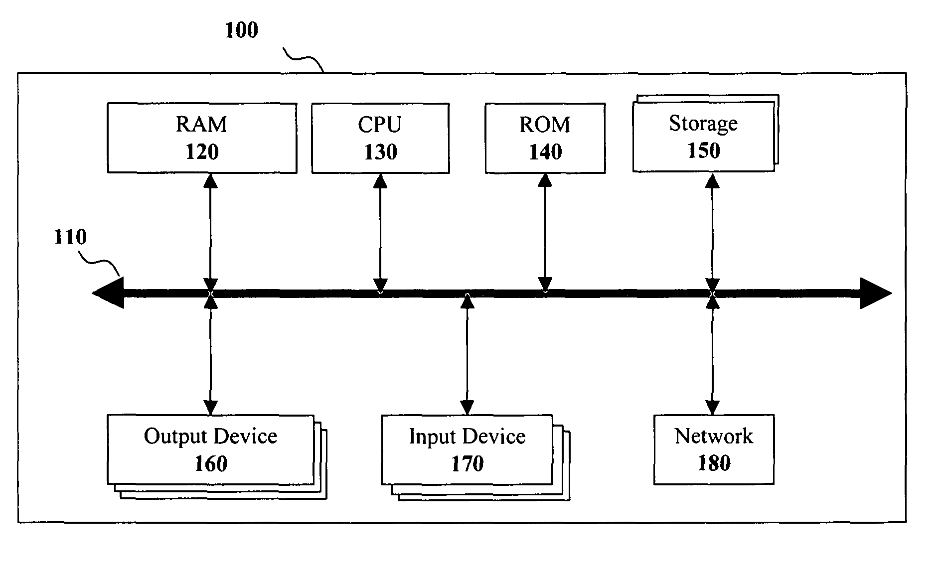
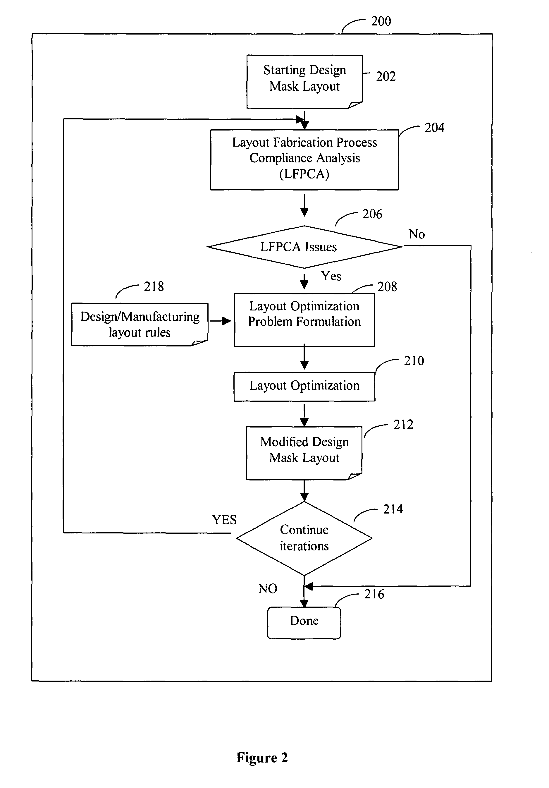
System and method of maximizing integrated circuit manufacturing yield with fabrication process simulation driven layout optimization
PatentInactiveUS7886262B2
Innovation
- A system and method for maximizing IC manufacturing yield through adaptive and iterative layout optimization driven by IC fabrication process simulation, utilizing layout fabrication process compliance analysis (LFPCA) to identify and mitigate issues, ensuring design rule correctness and reducing fabrication process issues while preserving design hierarchy and performance metrics.

System and Method for Artificial Intelligence Driven Fab-Technology Co-Optimization for Generation of Accurate Digital Twin Models for Simulation in Manufacturing and Design
PatentPendingUS20250021726A1
Innovation
- A physics and chemistry-based artificial intelligence-driven modeling tool and method that uses machine learning to create digital twin models of target devices, optimizing fabrication processes by reducing the number of input features, employing advanced Design of Experiments algorithms, and integrating data visualization, regression, and optimization modules to minimize time and cost.


Industry Standards for FAB Digital Twin Implementation
The semiconductor industry has recognized the critical need for standardized approaches to digital twin implementation in fabrication facilities, particularly as manufacturers seek to achieve ambitious yield improvement targets. Current industry standards are primarily driven by organizations such as SEMI, IEEE, and the International Technology Roadmap for Semiconductors (ITRS), which have established foundational frameworks for digital manufacturing systems integration.
SEMI E164 standard provides the fundamental architecture for equipment data collection and analysis, serving as a cornerstone for digital twin implementations. This standard defines the data structures and communication protocols necessary for real-time equipment monitoring and control. Additionally, SEMI E187 establishes guidelines for manufacturing execution system integration, enabling seamless data flow between physical fabrication equipment and digital simulation environments.
IEEE 1451 series standards address sensor integration and smart transducer interfaces, which are essential components for comprehensive digital twin systems. These standards ensure interoperability between different sensor technologies and data acquisition systems, facilitating the creation of accurate virtual representations of fabrication processes. The IEEE 1588 Precision Time Protocol standard ensures synchronized data collection across distributed manufacturing systems, maintaining temporal accuracy crucial for process correlation analysis.
The Industry 4.0 framework, particularly the Reference Architecture Model Industrie 4.0 (RAMI 4.0), provides a comprehensive structure for implementing cyber-physical systems in manufacturing environments. This framework addresses the hierarchical integration of digital twin systems from individual equipment level to entire fabrication facility operations, supporting the scalability requirements for yield optimization initiatives.
Emerging standards such as ISO 23247 specifically target digital twin manufacturing systems, defining requirements for digital twin frameworks, reference architecture, and implementation guidelines. This standard addresses data quality, model validation, and system interoperability aspects that are particularly relevant for substrate yield improvement applications.
The Open Platform Communications Unified Architecture (OPC UA) standard has become increasingly important for secure, reliable data exchange in industrial digital twin implementations. OPC UA provides the communication infrastructure necessary for real-time data synchronization between physical fabrication processes and their digital counterparts, enabling the continuous model updates required for accurate yield prediction and optimization.
Cost-Benefit Analysis of Digital Twin ROI in Manufacturing
The implementation of dedicated FAB digital twin simulations to achieve 2X substrate yield improvement presents a compelling investment opportunity with quantifiable returns across multiple operational dimensions. Initial capital expenditure typically ranges from $2-5 million for comprehensive digital twin infrastructure, including high-fidelity modeling software, computational hardware, and integration systems. However, the financial benefits substantially outweigh these upfront costs through direct yield improvements and operational efficiencies.
Direct yield enhancement from 85% to 95% baseline performance translates to immediate revenue gains of approximately $15-25 million annually for a typical 200mm wafer fabrication facility processing 10,000 wafers monthly. This calculation assumes average substrate values of $800-1,200 per unit, making the payback period remarkably short at 6-12 months. The digital twin's predictive capabilities reduce scrap rates by 40-60%, generating additional cost savings of $3-8 million per year through material waste reduction.
Operational cost reductions emerge through optimized process parameters and reduced equipment downtime. Digital twin simulations enable predictive maintenance strategies, decreasing unplanned equipment failures by 35-50% and reducing maintenance costs by $2-4 million annually. Energy consumption optimization through simulation-guided process adjustments typically yields 8-15% reduction in facility energy costs, contributing an additional $1-2 million in annual savings.
Risk mitigation benefits provide substantial but harder-to-quantify value. Digital twins reduce the probability of catastrophic process failures that could result in $10-50 million losses from contaminated production runs or equipment damage. The simulation environment enables risk-free testing of process modifications, eliminating costly physical trial-and-error approaches that historically consumed 15-25% of R&D budgets.
Long-term strategic advantages include accelerated time-to-market for new products, with development cycles shortened by 20-40% through virtual prototyping and optimization. This competitive advantage translates to market share gains and premium pricing opportunities worth $5-15 million annually. The cumulative five-year ROI typically exceeds 400-600%, establishing digital twin implementation as one of the highest-return manufacturing investments available.
Unlock deeper insights with PatSnap Eureka Quick Research — get a full tech report to explore trends and direct your research. Try now!
Generate Your Research Report Instantly with AI Agent
Supercharge your innovation with PatSnap Eureka AI Agent Platform!