
Integrated Parallel Plate Capacitors for High-Frequency Circuits: Optimization Tips
JUN 27, 20269 MIN READ
Generate Your Research Report Instantly with AI Agent
Patsnap Eureka helps you evaluate technical feasibility & market potential.
Integrated Capacitor Technology Background and Objectives
Integrated capacitor technology has emerged as a critical component in modern semiconductor manufacturing, driven by the relentless pursuit of miniaturization and performance enhancement in electronic systems. The evolution from discrete capacitive elements to fully integrated solutions represents a paradigm shift that began in the 1970s with early hybrid circuits and has accelerated dramatically with advanced CMOS processes. This technological progression reflects the industry's response to increasing demands for higher integration density, reduced parasitic effects, and improved high-frequency performance characteristics.
The development trajectory of integrated capacitors has been closely intertwined with semiconductor process advancements, particularly in deep submicron technologies. Early implementations relied on simple metal-oxide-semiconductor structures, but modern approaches leverage sophisticated dielectric materials, multi-layer metallization schemes, and three-dimensional architectures. The transition from aluminum-based to copper interconnect technologies has further expanded design possibilities, enabling more complex capacitor geometries and improved electrical characteristics.
Parallel plate capacitors represent the most fundamental and widely adopted configuration in integrated circuit design due to their predictable behavior, scalable geometry, and compatibility with standard fabrication processes. These structures consist of two conductive plates separated by a dielectric material, forming a capacitive element that can be precisely controlled through dimensional and material parameters. The simplicity of this architecture makes it particularly attractive for high-volume manufacturing while maintaining excellent electrical performance across various operating conditions.
The primary objectives driving current research and development efforts focus on achieving optimal performance in high-frequency applications where traditional design approaches often fall short. Key targets include minimizing parasitic inductance and resistance, maximizing quality factor across broad frequency ranges, and maintaining stable capacitance values under varying environmental conditions. Additionally, there is significant emphasis on developing design methodologies that can accurately predict and optimize capacitor behavior in complex RF and mixed-signal environments.
Contemporary optimization efforts concentrate on addressing the fundamental trade-offs between capacitance density, frequency response, and manufacturing feasibility. The challenge lies in balancing these competing requirements while maintaining compatibility with existing process flows and design rules. Advanced modeling techniques, including electromagnetic simulation and statistical analysis, have become essential tools for achieving these optimization goals and enabling predictive design capabilities that reduce development cycles and improve first-pass success rates.
The development trajectory of integrated capacitors has been closely intertwined with semiconductor process advancements, particularly in deep submicron technologies. Early implementations relied on simple metal-oxide-semiconductor structures, but modern approaches leverage sophisticated dielectric materials, multi-layer metallization schemes, and three-dimensional architectures. The transition from aluminum-based to copper interconnect technologies has further expanded design possibilities, enabling more complex capacitor geometries and improved electrical characteristics.
Parallel plate capacitors represent the most fundamental and widely adopted configuration in integrated circuit design due to their predictable behavior, scalable geometry, and compatibility with standard fabrication processes. These structures consist of two conductive plates separated by a dielectric material, forming a capacitive element that can be precisely controlled through dimensional and material parameters. The simplicity of this architecture makes it particularly attractive for high-volume manufacturing while maintaining excellent electrical performance across various operating conditions.
The primary objectives driving current research and development efforts focus on achieving optimal performance in high-frequency applications where traditional design approaches often fall short. Key targets include minimizing parasitic inductance and resistance, maximizing quality factor across broad frequency ranges, and maintaining stable capacitance values under varying environmental conditions. Additionally, there is significant emphasis on developing design methodologies that can accurately predict and optimize capacitor behavior in complex RF and mixed-signal environments.
Contemporary optimization efforts concentrate on addressing the fundamental trade-offs between capacitance density, frequency response, and manufacturing feasibility. The challenge lies in balancing these competing requirements while maintaining compatibility with existing process flows and design rules. Advanced modeling techniques, including electromagnetic simulation and statistical analysis, have become essential tools for achieving these optimization goals and enabling predictive design capabilities that reduce development cycles and improve first-pass success rates.
High-Frequency Circuit Market Demand Analysis
The high-frequency circuit market is experiencing unprecedented growth driven by the proliferation of wireless communication technologies, including 5G networks, Internet of Things (IoT) devices, and advanced radar systems. This expansion has created substantial demand for sophisticated circuit components capable of operating efficiently at frequencies ranging from several gigahertz to terahertz levels.
Telecommunications infrastructure represents the largest segment driving market demand, with 5G base stations requiring high-performance capacitors that maintain stable electrical characteristics across wide frequency ranges. The deployment of millimeter-wave communication systems necessitates components with minimal parasitic effects and precise impedance control, making integrated parallel plate capacitors increasingly critical for signal integrity.
Consumer electronics markets are simultaneously pushing demand through the integration of high-frequency circuits in smartphones, tablets, and wearable devices. These applications require miniaturized components that deliver consistent performance while occupying minimal board space. The trend toward higher data transmission rates and reduced power consumption further amplifies the need for optimized capacitive elements.
Automotive electronics present another significant growth driver, particularly with the advancement of autonomous driving technologies and vehicle-to-everything communication systems. High-frequency radar sensors, LiDAR systems, and advanced driver assistance systems rely heavily on precise timing and filtering circuits where integrated parallel plate capacitors play essential roles.
The aerospace and defense sectors continue to demand high-reliability components for satellite communications, electronic warfare systems, and advanced radar applications. These markets require capacitors that maintain performance under extreme environmental conditions while operating at increasingly higher frequencies.
Medical device applications, including wireless patient monitoring systems and high-resolution imaging equipment, contribute to market expansion by requiring components that minimize electromagnetic interference while ensuring signal clarity. The growing telemedicine sector further accelerates demand for reliable high-frequency circuit components.
Market analysis indicates that the convergence of these application areas is creating opportunities for integrated solutions that combine multiple functions within single components, driving innovation in parallel plate capacitor design and manufacturing processes.
Telecommunications infrastructure represents the largest segment driving market demand, with 5G base stations requiring high-performance capacitors that maintain stable electrical characteristics across wide frequency ranges. The deployment of millimeter-wave communication systems necessitates components with minimal parasitic effects and precise impedance control, making integrated parallel plate capacitors increasingly critical for signal integrity.
Consumer electronics markets are simultaneously pushing demand through the integration of high-frequency circuits in smartphones, tablets, and wearable devices. These applications require miniaturized components that deliver consistent performance while occupying minimal board space. The trend toward higher data transmission rates and reduced power consumption further amplifies the need for optimized capacitive elements.
Automotive electronics present another significant growth driver, particularly with the advancement of autonomous driving technologies and vehicle-to-everything communication systems. High-frequency radar sensors, LiDAR systems, and advanced driver assistance systems rely heavily on precise timing and filtering circuits where integrated parallel plate capacitors play essential roles.
The aerospace and defense sectors continue to demand high-reliability components for satellite communications, electronic warfare systems, and advanced radar applications. These markets require capacitors that maintain performance under extreme environmental conditions while operating at increasingly higher frequencies.
Medical device applications, including wireless patient monitoring systems and high-resolution imaging equipment, contribute to market expansion by requiring components that minimize electromagnetic interference while ensuring signal clarity. The growing telemedicine sector further accelerates demand for reliable high-frequency circuit components.
Market analysis indicates that the convergence of these application areas is creating opportunities for integrated solutions that combine multiple functions within single components, driving innovation in parallel plate capacitor design and manufacturing processes.
Current State of Parallel Plate Capacitor Integration
The integration of parallel plate capacitors in high-frequency circuits has reached a mature stage in semiconductor manufacturing, with current technologies achieving remarkable miniaturization and performance optimization. Modern fabrication processes enable the production of integrated parallel plate capacitors with capacitance values ranging from femtofarads to several picofarads, utilizing advanced dielectric materials such as silicon dioxide, silicon nitride, and high-k materials like hafnium oxide and tantalum pentoxide.
Contemporary manufacturing techniques predominantly employ CMOS-compatible processes, allowing seamless integration with existing semiconductor fabrication lines. The most widely adopted approach involves metal-insulator-metal (MIM) structures, where thin dielectric layers are sandwiched between precisely patterned metal electrodes. Current process nodes support dielectric thicknesses as thin as 10-50 nanometers, enabling high capacitance density while maintaining acceptable leakage currents and breakdown voltages.
Leading semiconductor foundries have successfully implemented multi-layer capacitor architectures, stacking multiple parallel plate structures to increase capacitance density without expanding the footprint. These three-dimensional integration approaches utilize through-silicon vias and advanced interconnect technologies to maintain low parasitic resistance and inductance, critical for high-frequency performance.
The current state of parallel plate capacitor integration faces several technical constraints that limit optimal performance in high-frequency applications. Parasitic effects, including series resistance from metal interconnects and substrate coupling, continue to challenge designers working above gigahertz frequencies. Additionally, process variations in dielectric thickness and electrode alignment introduce capacitance matching issues, particularly problematic in precision analog circuits and phase-locked loops.
Temperature stability remains a significant concern, as current dielectric materials exhibit temperature coefficients that can cause substantial capacitance drift across operating ranges. This limitation necessitates complex compensation schemes or restricts the operating temperature range of high-precision circuits. Furthermore, the trade-off between breakdown voltage and capacitance density constrains the design space for power-sensitive applications.
Manufacturing yield considerations also impact the current integration landscape, as defect densities in ultra-thin dielectrics can significantly affect production economics. The industry continues to address these challenges through improved process control, advanced metrology techniques, and novel dielectric material development to enhance the reliability and performance of integrated parallel plate capacitors in next-generation high-frequency circuit applications.
Contemporary manufacturing techniques predominantly employ CMOS-compatible processes, allowing seamless integration with existing semiconductor fabrication lines. The most widely adopted approach involves metal-insulator-metal (MIM) structures, where thin dielectric layers are sandwiched between precisely patterned metal electrodes. Current process nodes support dielectric thicknesses as thin as 10-50 nanometers, enabling high capacitance density while maintaining acceptable leakage currents and breakdown voltages.
Leading semiconductor foundries have successfully implemented multi-layer capacitor architectures, stacking multiple parallel plate structures to increase capacitance density without expanding the footprint. These three-dimensional integration approaches utilize through-silicon vias and advanced interconnect technologies to maintain low parasitic resistance and inductance, critical for high-frequency performance.
The current state of parallel plate capacitor integration faces several technical constraints that limit optimal performance in high-frequency applications. Parasitic effects, including series resistance from metal interconnects and substrate coupling, continue to challenge designers working above gigahertz frequencies. Additionally, process variations in dielectric thickness and electrode alignment introduce capacitance matching issues, particularly problematic in precision analog circuits and phase-locked loops.
Temperature stability remains a significant concern, as current dielectric materials exhibit temperature coefficients that can cause substantial capacitance drift across operating ranges. This limitation necessitates complex compensation schemes or restricts the operating temperature range of high-precision circuits. Furthermore, the trade-off between breakdown voltage and capacitance density constrains the design space for power-sensitive applications.
Manufacturing yield considerations also impact the current integration landscape, as defect densities in ultra-thin dielectrics can significantly affect production economics. The industry continues to address these challenges through improved process control, advanced metrology techniques, and novel dielectric material development to enhance the reliability and performance of integrated parallel plate capacitors in next-generation high-frequency circuit applications.
Current Parallel Plate Capacitor Design Solutions
01 Integrated capacitor structures in semiconductor devices
Integration of parallel plate capacitors directly into semiconductor substrates and integrated circuits to provide on-chip capacitance. These structures utilize metal layers separated by dielectric materials to form capacitive elements that can be manufactured using standard semiconductor fabrication processes. The integration allows for compact designs and improved electrical performance in electronic devices.- Integrated capacitor structures in semiconductor devices: Integration of parallel plate capacitors directly into semiconductor substrates and integrated circuits to provide on-chip capacitance. These structures utilize semiconductor fabrication processes to create capacitive elements that can be embedded within the device architecture, offering compact solutions for energy storage and signal processing applications.
- Multi-layer parallel plate capacitor configurations: Advanced capacitor designs featuring multiple parallel plate layers stacked vertically or arranged in complex geometries to maximize capacitance density. These configurations optimize the use of available space while maintaining electrical performance through careful layer spacing and material selection.
- Dielectric materials and insulation systems: Specialized dielectric materials and insulation systems designed for parallel plate capacitors to enhance electrical performance and reliability. These materials provide optimal dielectric constants, breakdown voltages, and temperature stability for various applications while ensuring proper isolation between conductive plates.
- Manufacturing processes and fabrication techniques: Specialized manufacturing methods for producing integrated parallel plate capacitors, including photolithography, etching, deposition, and assembly processes. These techniques enable precise control over capacitor dimensions, material properties, and electrical characteristics during production.
- Applications in electronic circuits and systems: Implementation of integrated parallel plate capacitors in various electronic applications including power management, signal filtering, timing circuits, and energy storage systems. These applications leverage the compact size and reliable performance of integrated capacitors for improved system functionality.
02 Multi-layer capacitor configurations
Design and fabrication of capacitors with multiple parallel plate layers stacked vertically to increase capacitance density within a given footprint. These configurations utilize alternating conductive and dielectric layers to create multiple capacitive elements in a single integrated structure, enabling higher capacitance values in compact form factors.Expand Specific Solutions03 Dielectric materials and insulation layers
Development and optimization of dielectric materials used between parallel plates to enhance capacitor performance. Focus on materials with high dielectric constants, low leakage currents, and thermal stability. The selection and processing of these materials directly impacts the electrical characteristics and reliability of the integrated capacitors.Expand Specific Solutions04 Electrode design and metallization schemes
Engineering of conductive plates and electrode structures for optimal electrical contact and field distribution in integrated capacitors. This includes the design of metal interconnects, contact areas, and geometric configurations that minimize parasitic effects while maximizing capacitive coupling between parallel plates.Expand Specific Solutions05 Manufacturing processes and fabrication methods
Specialized manufacturing techniques for creating integrated parallel plate capacitors including etching, deposition, lithography, and assembly processes. These methods ensure precise dimensional control, material uniformity, and integration compatibility with existing semiconductor manufacturing workflows while maintaining high yield and reliability.Expand Specific Solutions
Key Players in RF IC and Capacitor Industry
The integrated parallel plate capacitor market for high-frequency circuits represents a mature yet rapidly evolving sector within the broader semiconductor industry, currently valued at several billion dollars with steady growth driven by 5G, automotive electronics, and IoT applications. The competitive landscape is dominated by established semiconductor giants and specialized component manufacturers operating at different technological maturity levels. Leading players like Intel, Samsung Electronics, and Taiwan Semiconductor Manufacturing demonstrate advanced integration capabilities, while companies such as Murata Manufacturing, TDK Corp., and Texas Instruments excel in specialized passive component technologies. Mid-tier competitors including Infineon Technologies, MediaTek, and Qualcomm focus on application-specific optimizations, particularly for mobile and automotive markets. The technology has reached commercial maturity in standard applications, though innovation continues in areas like GaN-based solutions from companies like Efficient Power Conversion Corp. and advanced packaging techniques from foundries like GlobalFoundries.
Intel Corp.
Technical Solution: Intel integrates parallel plate capacitors directly into their semiconductor packaging and on-die solutions for high-frequency processor and chipset applications. Their technology focuses on metal-insulator-metal (MIM) capacitor structures fabricated using advanced semiconductor processes, enabling precise control over capacitance density and electrical characteristics. Intel's approach includes deep trench capacitors and planar capacitor arrays integrated within the silicon substrate or package substrate layers, optimized for power delivery networks and high-speed signal conditioning. The company utilizes high-k dielectric materials and advanced lithography techniques to achieve high capacitance density while minimizing parasitic effects, particularly targeting applications in processors, memory interfaces, and high-speed digital circuits operating at multi-gigahertz frequencies.
Strengths: Advanced semiconductor fabrication capabilities enabling precise integration and high-density solutions. Weaknesses: Limited to specific applications within Intel's ecosystem and high development costs for custom solutions.
Murata Manufacturing Co. Ltd.
Technical Solution: Murata specializes in multilayer ceramic capacitors (MLCCs) with integrated parallel plate structures optimized for high-frequency applications. Their technology focuses on low equivalent series resistance (ESR) and equivalent series inductance (ESL) designs, utilizing advanced ceramic dielectric materials and precise electrode patterning. The company employs proprietary firing techniques and material compositions to achieve capacitance values ranging from picofarads to microfarads while maintaining stable performance at frequencies up to several GHz. Their integrated approach includes co-fired ceramic substrates that allow multiple capacitors to be embedded within the same package, reducing parasitic effects and improving signal integrity in RF circuits.
Strengths: Industry-leading MLCC technology with excellent high-frequency characteristics and miniaturization capabilities. Weaknesses: Higher cost compared to discrete solutions and limited customization options for specialized applications.
Core Patents in High-Frequency Capacitor Optimization
Integrated parallel plate capacitors
PatentInactiveUS20070190760A1
Innovation
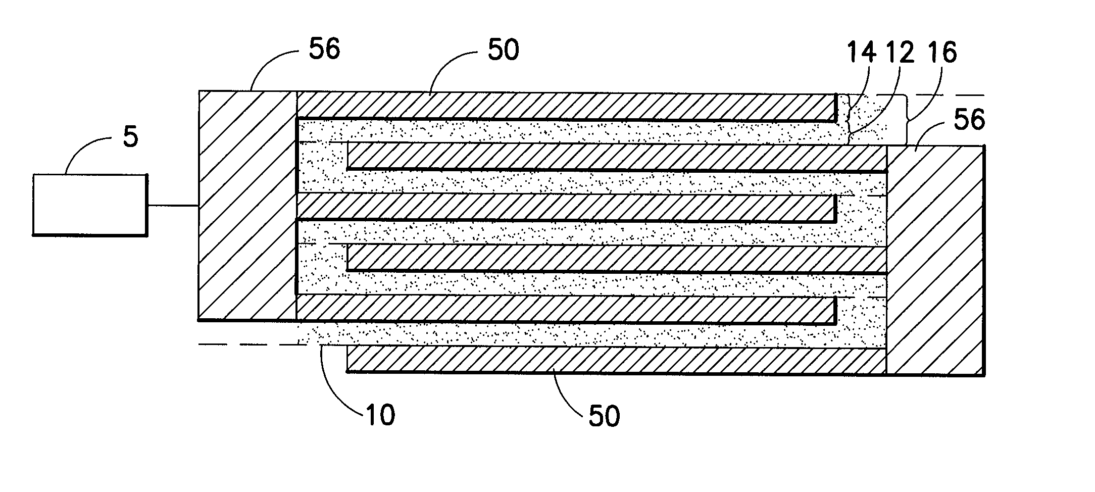
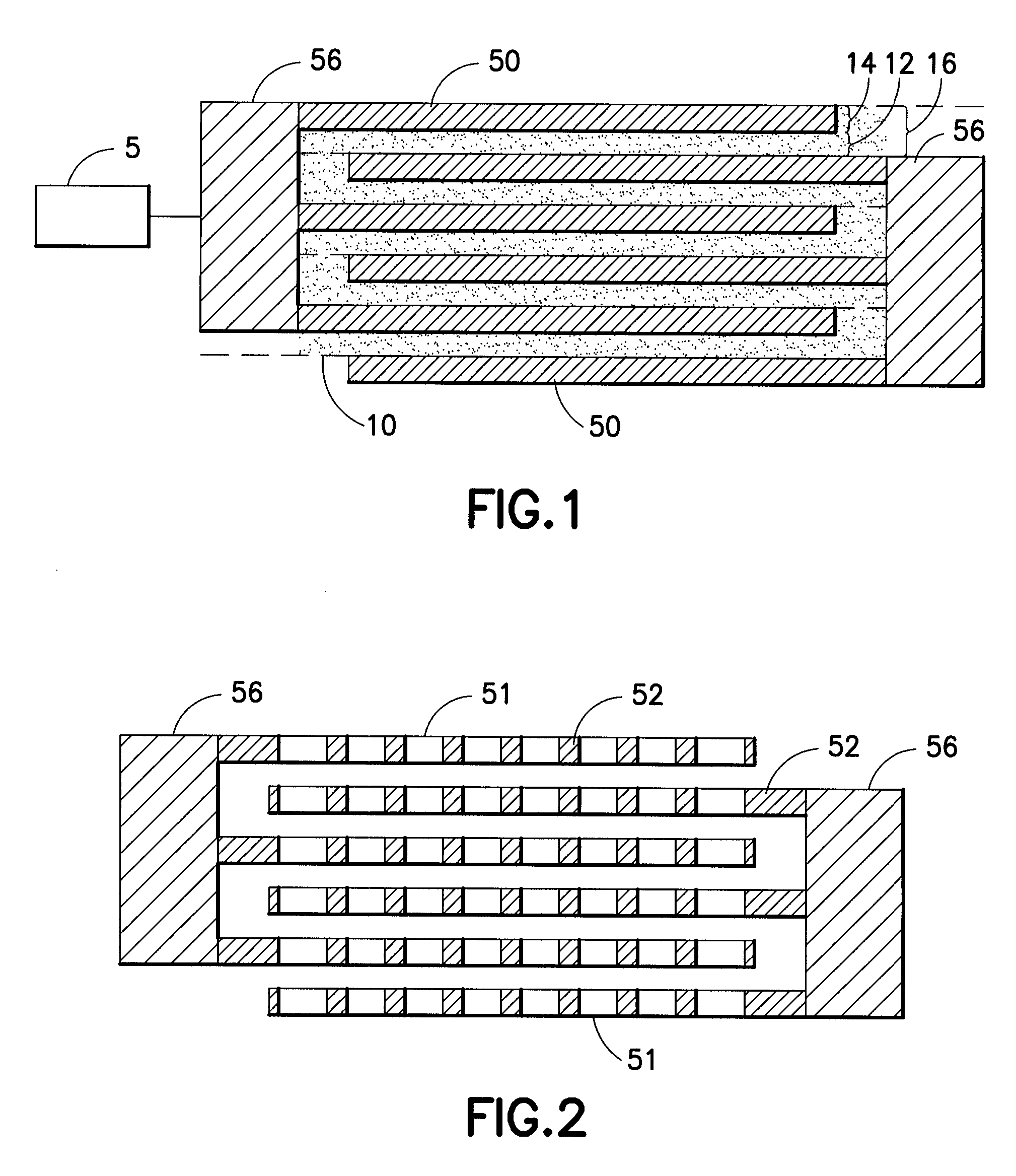
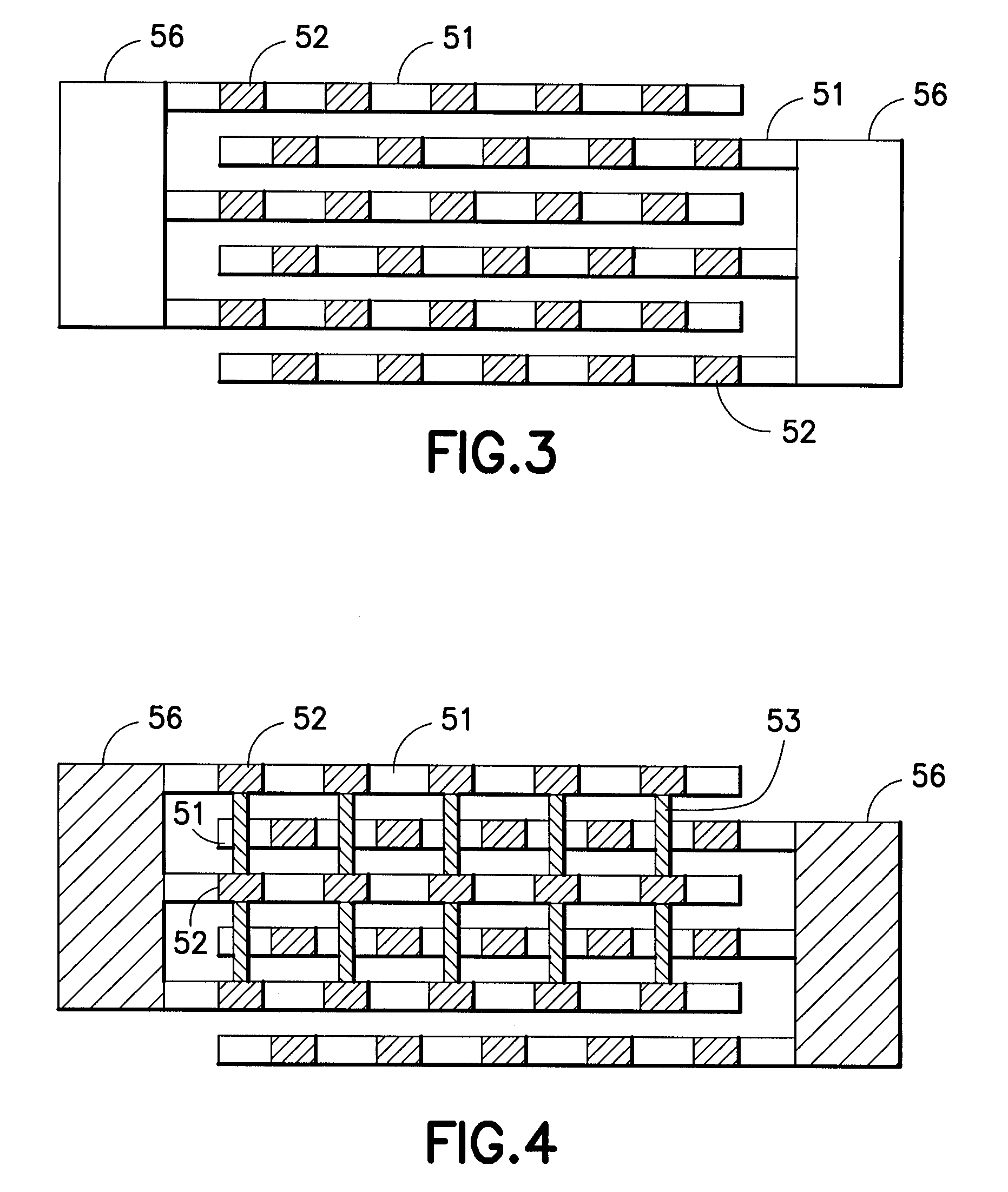
- The use of BEOL wide Cu planes as MIM capacitor electrodes with existing inter-level dielectric layers and the addition of through-vias through perforation holes to create a high-Q MIM capacitor, reducing plate resistance and enhancing capacitance density without additional processing steps or masks.

Dampening of electric field-induced resonance in parallel plate capacitors
PatentActiveUS20070025058A1
Innovation
- An additional mass layer, such as gold, platinum, or tungsten, is applied on top of the capacitor to dampen resonant vibrations, decoupling physical resonance from RF signal frequencies by reducing mechanical vibrations through a mass-spring model analogy.


Manufacturing Process Optimization Strategies
Manufacturing process optimization for integrated parallel plate capacitors in high-frequency circuits requires a systematic approach that addresses both material selection and fabrication precision. The primary focus centers on achieving consistent dielectric thickness, minimizing parasitic effects, and ensuring reliable electrical performance across varying operational frequencies.
Substrate preparation represents the foundational step in optimization strategies. Advanced cleaning protocols utilizing plasma treatment and chemical etching ensure optimal surface conditions for subsequent layer deposition. The substrate surface roughness must be controlled within nanometer tolerances to prevent field concentration effects that could compromise capacitor performance at high frequencies.
Dielectric layer deposition demands precise control over thickness uniformity and material properties. Atomic layer deposition and chemical vapor deposition techniques offer superior thickness control compared to traditional sputtering methods. Process parameters including temperature, pressure, and precursor flow rates require careful optimization to achieve target dielectric constants while minimizing loss tangent values.
Metal electrode formation involves critical considerations for conductor resistivity and interface quality. Advanced photolithography techniques enable precise pattern definition, while optimized etching processes ensure clean edge profiles that minimize fringing field effects. The selection of barrier layers and adhesion promoters significantly impacts long-term reliability and electrical stability.
Thermal management during processing plays a crucial role in maintaining dimensional stability and preventing stress-induced defects. Controlled annealing cycles help optimize crystal structure in dielectric materials while relieving mechanical stress at interfaces. Temperature ramping profiles must be carefully designed to prevent thermal shock and ensure uniform heating across large substrate areas.
Quality control integration throughout the manufacturing flow enables real-time process adjustments and defect prevention. In-line metrology systems monitor critical parameters including layer thickness, surface roughness, and electrical properties. Statistical process control methodologies help identify process variations before they impact final device performance, ensuring consistent manufacturing yields and reliable high-frequency operation.
Substrate preparation represents the foundational step in optimization strategies. Advanced cleaning protocols utilizing plasma treatment and chemical etching ensure optimal surface conditions for subsequent layer deposition. The substrate surface roughness must be controlled within nanometer tolerances to prevent field concentration effects that could compromise capacitor performance at high frequencies.
Dielectric layer deposition demands precise control over thickness uniformity and material properties. Atomic layer deposition and chemical vapor deposition techniques offer superior thickness control compared to traditional sputtering methods. Process parameters including temperature, pressure, and precursor flow rates require careful optimization to achieve target dielectric constants while minimizing loss tangent values.
Metal electrode formation involves critical considerations for conductor resistivity and interface quality. Advanced photolithography techniques enable precise pattern definition, while optimized etching processes ensure clean edge profiles that minimize fringing field effects. The selection of barrier layers and adhesion promoters significantly impacts long-term reliability and electrical stability.
Thermal management during processing plays a crucial role in maintaining dimensional stability and preventing stress-induced defects. Controlled annealing cycles help optimize crystal structure in dielectric materials while relieving mechanical stress at interfaces. Temperature ramping profiles must be carefully designed to prevent thermal shock and ensure uniform heating across large substrate areas.
Quality control integration throughout the manufacturing flow enables real-time process adjustments and defect prevention. In-line metrology systems monitor critical parameters including layer thickness, surface roughness, and electrical properties. Statistical process control methodologies help identify process variations before they impact final device performance, ensuring consistent manufacturing yields and reliable high-frequency operation.
Parasitic Effects Mitigation Techniques
Parasitic effects in integrated parallel plate capacitors represent one of the most critical challenges in high-frequency circuit design, significantly impacting performance and reliability. These unwanted electrical phenomena manifest as parasitic inductance, resistance, and coupling effects that can severely degrade circuit functionality at elevated frequencies. The primary parasitic elements include series resistance from metallization layers, parasitic inductance from current paths, and substrate coupling effects that introduce unwanted signal interactions.
Series resistance mitigation requires careful attention to metallization design and material selection. Implementing thicker metal layers with low-resistivity materials such as copper significantly reduces ohmic losses. Multi-layer metallization schemes with parallel current paths effectively distribute current flow, minimizing resistance-induced voltage drops. Advanced fabrication techniques utilizing electroplating processes enable the creation of thick, uniform metal layers that maintain low resistance characteristics across wide frequency ranges.
Parasitic inductance control demands strategic layout optimization and geometric considerations. Minimizing current loop areas through careful routing and ground plane placement reduces inductive effects. Implementing multiple via connections in parallel between capacitor plates and ground planes creates low-inductance current paths. The use of differential signaling techniques with symmetric layouts helps cancel common-mode inductance while maintaining signal integrity.
Substrate coupling mitigation involves sophisticated isolation techniques and material engineering approaches. Deep trench isolation structures create physical barriers that prevent unwanted signal propagation through the substrate. Guard ring implementations with proper biasing schemes provide effective isolation between sensitive circuit blocks. High-resistivity substrate materials or silicon-on-insulator technologies offer superior isolation characteristics, reducing parasitic coupling effects significantly.
Advanced shielding techniques play crucial roles in minimizing electromagnetic interference and crosstalk. Faraday cage structures implemented through multi-layer metallization provide comprehensive electromagnetic shielding. Grounded metal shields positioned strategically around capacitor structures prevent field coupling between adjacent components. Proper shield grounding through low-impedance connections ensures effective field containment and noise suppression.
Layout optimization strategies focus on minimizing parasitic effects through intelligent placement and routing decisions. Symmetric layouts with matched current paths reduce differential parasitic effects. Strategic component placement considering electromagnetic field distributions minimizes unwanted coupling mechanisms. Implementation of kelvin connections for critical measurements ensures accurate characterization while minimizing measurement-induced parasitics.
Series resistance mitigation requires careful attention to metallization design and material selection. Implementing thicker metal layers with low-resistivity materials such as copper significantly reduces ohmic losses. Multi-layer metallization schemes with parallel current paths effectively distribute current flow, minimizing resistance-induced voltage drops. Advanced fabrication techniques utilizing electroplating processes enable the creation of thick, uniform metal layers that maintain low resistance characteristics across wide frequency ranges.
Parasitic inductance control demands strategic layout optimization and geometric considerations. Minimizing current loop areas through careful routing and ground plane placement reduces inductive effects. Implementing multiple via connections in parallel between capacitor plates and ground planes creates low-inductance current paths. The use of differential signaling techniques with symmetric layouts helps cancel common-mode inductance while maintaining signal integrity.
Substrate coupling mitigation involves sophisticated isolation techniques and material engineering approaches. Deep trench isolation structures create physical barriers that prevent unwanted signal propagation through the substrate. Guard ring implementations with proper biasing schemes provide effective isolation between sensitive circuit blocks. High-resistivity substrate materials or silicon-on-insulator technologies offer superior isolation characteristics, reducing parasitic coupling effects significantly.
Advanced shielding techniques play crucial roles in minimizing electromagnetic interference and crosstalk. Faraday cage structures implemented through multi-layer metallization provide comprehensive electromagnetic shielding. Grounded metal shields positioned strategically around capacitor structures prevent field coupling between adjacent components. Proper shield grounding through low-impedance connections ensures effective field containment and noise suppression.
Layout optimization strategies focus on minimizing parasitic effects through intelligent placement and routing decisions. Symmetric layouts with matched current paths reduce differential parasitic effects. Strategic component placement considering electromagnetic field distributions minimizes unwanted coupling mechanisms. Implementation of kelvin connections for critical measurements ensures accurate characterization while minimizing measurement-induced parasitics.
Unlock deeper insights with Patsnap Eureka Quick Research — get a full tech report to explore trends and direct your research. Try now!
Generate Your Research Report Instantly with AI Agent
Supercharge your innovation with Patsnap Eureka AI Agent Platform!