Maximizing Light Efficiency in Wafer-Level Optics for LED Systems
APR 9, 20269 MIN READ
Generate Your Research Report Instantly with AI Agent
Patsnap Eureka helps you evaluate technical feasibility & market potential.
LED Wafer-Level Optics Background and Efficiency Goals
LED wafer-level optics represents a paradigm shift in solid-state lighting technology, emerging from the convergence of semiconductor manufacturing and precision optical engineering. This approach integrates optical elements directly onto LED wafer substrates during the fabrication process, eliminating traditional discrete optical components and enabling unprecedented miniaturization and performance optimization. The technology builds upon decades of LED development, from early gallium arsenide phosphide devices in the 1960s to modern high-brightness InGaN-based systems.
The evolution of LED technology has consistently pursued higher luminous efficacy, with laboratory demonstrations exceeding 300 lumens per watt and commercial products achieving 150-200 lm/W. However, traditional LED packaging and secondary optics introduce significant efficiency losses, typically reducing system-level performance by 20-40%. Wafer-level optics addresses these limitations by implementing optical functionality at the chip level, minimizing interfaces and optimizing light extraction from the semiconductor junction.
Current market demands for LED systems emphasize not only efficiency but also form factor reduction, cost optimization, and enhanced optical control. Applications ranging from mobile device backlighting to automotive headlamps require increasingly sophisticated light management capabilities within constrained spatial envelopes. Wafer-level optics enables these requirements by providing precise beam shaping, color mixing, and intensity distribution control directly at the source.
The primary efficiency goals for wafer-level LED optics encompass multiple performance metrics. Light extraction efficiency targets focus on maximizing photon escape from high-refractive-index semiconductor materials, addressing total internal reflection losses that can trap up to 80% of generated light. Optical coupling efficiency aims to minimize losses during light transfer between different optical elements and interfaces within the integrated system.
Thermal management represents another critical efficiency objective, as wafer-level integration must maintain junction temperatures below critical thresholds while maximizing optical output. Advanced thermal interface materials and heat spreading structures integrated at the wafer level contribute to overall system efficiency by enabling higher drive currents and sustained performance.
Manufacturing scalability and yield optimization constitute essential goals for commercial viability. Wafer-level processes must achieve high uniformity across large substrate areas while maintaining precise optical tolerances. Cost reduction through batch processing and elimination of discrete assembly steps drives the economic justification for this technological approach, targeting 30-50% cost reductions compared to conventional LED packaging methods.
Market Demand for High-Efficiency LED Lighting Systems
The global LED lighting market has experienced unprecedented growth driven by increasing energy efficiency requirements and environmental sustainability mandates. Government regulations worldwide are phasing out traditional incandescent and fluorescent lighting systems, creating substantial demand for high-performance LED solutions. Energy efficiency standards such as ENERGY STAR and European Union regulations have established minimum efficacy requirements that push manufacturers toward advanced optical technologies.
Commercial and industrial sectors represent the largest growth segments for high-efficiency LED systems. Office buildings, manufacturing facilities, and retail spaces are rapidly adopting LED lighting to reduce operational costs and meet corporate sustainability goals. The demand extends beyond simple replacement applications to sophisticated lighting systems that require precise light distribution and maximum photon extraction efficiency.
Automotive lighting applications have emerged as a critical market driver for wafer-level optics technology. Modern vehicles increasingly rely on LED systems for headlights, taillights, and interior illumination, where space constraints and thermal management challenges necessitate highly efficient optical designs. The automotive industry's shift toward electric vehicles further amplifies the need for energy-efficient lighting solutions to preserve battery life.
Consumer electronics markets, particularly smartphones, tablets, and display backlighting systems, demand compact LED solutions with superior light extraction capabilities. These applications require wafer-level optical components that can maximize brightness while minimizing power consumption and heat generation within extremely confined spaces.
The horticultural lighting sector has created new demand patterns for specialized LED systems optimized for plant growth applications. Indoor farming and greenhouse operations require high-efficiency lighting solutions that can deliver specific spectral outputs while maintaining cost-effective operation over extended periods.
Smart city initiatives and infrastructure modernization projects worldwide are driving demand for intelligent LED street lighting systems. These applications require robust, high-efficiency optical designs capable of providing uniform light distribution while supporting advanced control systems and sensors.
Market research indicates that lighting efficiency improvements directly correlate with adoption rates across all sectors. End users consistently prioritize solutions that offer superior lumens-per-watt performance, creating sustained demand for advanced wafer-level optical technologies that can maximize light extraction and minimize optical losses in LED systems.
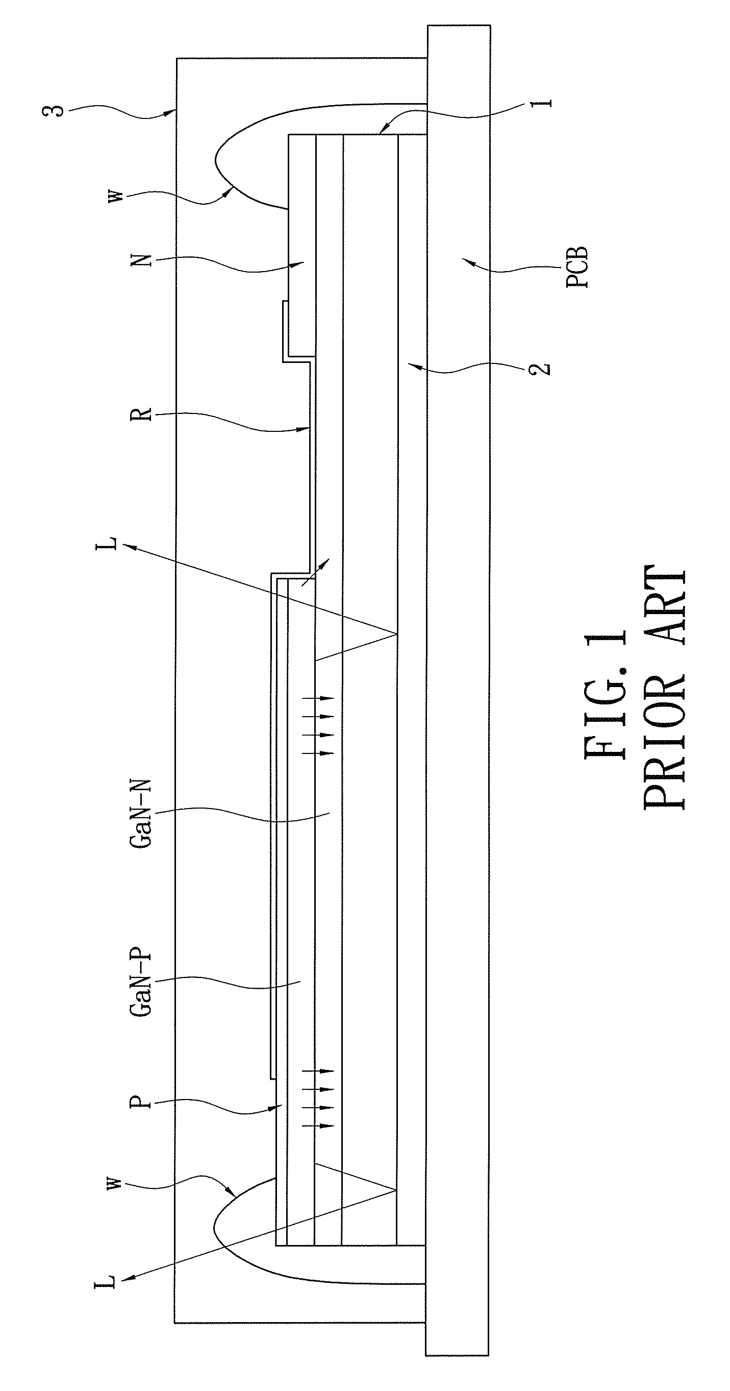
Current State and Light Loss Challenges in WLO
Wafer-level optics (WLO) technology has emerged as a critical manufacturing approach for LED systems, offering significant advantages in miniaturization, cost reduction, and mass production capabilities. However, the current state of WLO implementation faces substantial challenges in maintaining optimal light efficiency, with various loss mechanisms significantly impacting overall system performance.
The primary light loss mechanisms in WLO-based LED systems stem from multiple sources throughout the optical path. Surface reflection losses occur at each optical interface, typically accounting for 4-8% loss per surface in uncoated systems. These losses are particularly pronounced in multi-element WLO assemblies where light encounters numerous air-glass interfaces. Additionally, material absorption within the optical substrates contributes to cumulative losses, especially in thicker wafer configurations where light travels longer paths through the medium.
Fabrication-induced imperfections represent another significant challenge in current WLO implementations. Surface roughness from wafer processing, typically ranging from 10-50 nanometers RMS, creates scattering centers that redirect light away from intended optical paths. Replication accuracy limitations in molding processes introduce form errors that degrade optical performance, with typical tolerances of ±2-5 micrometers affecting critical optical surfaces.
Alignment precision issues compound these challenges, as WLO systems require extremely tight tolerances between LED chips and optical elements. Current assembly techniques achieve positioning accuracies of ±10-20 micrometers, which can result in 15-25% efficiency losses in high-numerical-aperture systems. The wafer-level nature of processing, while enabling cost-effective mass production, inherently limits the ability to perform individual element optimization and correction.
Thermal management presents additional complications in WLO systems. Heat generated by LED operation causes thermal expansion mismatches between different materials, leading to stress-induced birefringence and potential delamination at bonding interfaces. These thermal effects can reduce light transmission by 5-15% under typical operating conditions.
Current anti-reflection coating technologies, while partially addressing surface losses, face limitations in WLO applications. Traditional coating processes struggle with the complex three-dimensional geometries typical in WLO elements, resulting in non-uniform coating thickness and reduced effectiveness. The wafer-level processing constraints also limit coating material choices and deposition techniques.
Edge effects and light leakage represent emerging challenges as WLO systems become more compact. Light rays at extreme angles often escape through wafer edges or experience total internal reflection conditions that trap light within the substrate, reducing extraction efficiency by 10-20% in typical configurations.
Existing Solutions for LED Light Efficiency Optimization
01 Wafer-level lens array fabrication and integration
Wafer-level optics involves fabricating lens arrays directly on wafer substrates to improve light efficiency. This approach enables precise alignment and integration of optical elements at the wafer scale, reducing assembly complexity and optical losses. The technology allows for mass production of miniaturized optical systems with enhanced light transmission and collection efficiency through optimized lens geometries and anti-reflection coatings applied during wafer processing.- Wafer-level lens array fabrication and integration: Wafer-level optics involves fabricating lens arrays directly on wafer substrates to improve light efficiency. This approach enables precise alignment and integration of optical elements at the wafer scale, reducing assembly complexity and optical losses. The technology includes replication techniques, molding processes, and direct patterning methods to create microlens arrays with optimized optical properties. These fabrication methods enhance light collection efficiency and transmission by minimizing interface losses and improving optical coupling between components.
- Anti-reflective coatings and surface treatments: Applying specialized coatings and surface treatments to wafer-level optical components significantly improves light efficiency by reducing reflection losses. These treatments include multi-layer anti-reflective coatings, nanostructured surfaces, and index-matching layers that minimize Fresnel reflections at optical interfaces. Surface modification techniques optimize light transmission across different wavelength ranges and incident angles, enhancing overall optical performance in imaging and sensing applications.
- Optical element geometry and shape optimization: Optimizing the geometric design and shape profiles of wafer-level optical elements enhances light collection and focusing efficiency. This includes designing aspherical lens profiles, freeform surfaces, and customized curvatures that reduce aberrations and improve light concentration. Advanced computational modeling and simulation tools enable the optimization of optical element dimensions, spacing, and configurations to maximize light throughput and minimize losses in compact wafer-level packages.
- Material selection and refractive index engineering: Selecting appropriate optical materials with optimized refractive indices and transmission properties is crucial for improving light efficiency in wafer-level optics. This involves using high-transparency polymers, specialized glasses, and hybrid materials that offer superior optical performance. Material engineering techniques include gradient index materials, composite structures, and materials with tailored dispersion characteristics that enhance light coupling efficiency and reduce chromatic aberrations across the optical system.
- Packaging and alignment techniques for light efficiency: Advanced packaging and precision alignment methods at the wafer level are essential for maximizing light efficiency in optical systems. These techniques include active alignment processes, self-alignment structures, and integrated spacer designs that ensure optimal positioning of optical components. Packaging innovations incorporate light-guiding structures, reflective elements, and optimized aperture designs that minimize stray light and maximize useful light transmission. These approaches reduce coupling losses and improve overall system efficiency in compact wafer-level optical modules.
02 Micro-lens and diffractive optical elements for light coupling
Micro-lens arrays and diffractive optical elements fabricated at wafer level can significantly enhance light coupling efficiency. These structures are designed to focus, collimate, or redirect light with minimal losses, improving overall system performance. The integration of such elements directly onto image sensors or light sources at the wafer level eliminates alignment errors and reduces Fresnel reflection losses, thereby maximizing light efficiency in compact optical systems.Expand Specific Solutions03 Anti-reflection coatings and surface treatments
Application of anti-reflection coatings and specialized surface treatments at the wafer level is crucial for improving light efficiency. These coatings minimize reflection losses at optical interfaces and enhance light transmission through the optical system. Various coating materials and deposition techniques are employed during wafer-level processing to optimize spectral performance and reduce unwanted reflections, thereby increasing the overall light throughput of the optical system.Expand Specific Solutions04 Optical aperture optimization and light collection structures
Optimizing optical apertures and implementing specialized light collection structures at the wafer level can dramatically improve light efficiency. This includes designing and fabricating light guides, concentrators, and collection optics that maximize the capture and transmission of light. Wafer-level fabrication techniques enable precise control over aperture dimensions and collection angles, reducing vignetting and improving fill factor, which directly translates to enhanced light efficiency in imaging and sensing applications.Expand Specific Solutions05 Refractive index matching and optical bonding techniques
Wafer-level optical bonding and refractive index matching techniques are employed to minimize interface losses and improve light transmission efficiency. By carefully selecting bonding materials and processes that match the refractive indices of adjacent optical components, reflection losses at interfaces can be significantly reduced. These techniques enable the creation of monolithic optical systems with improved light efficiency through elimination of air gaps and optimization of optical path continuity throughout the wafer-level assembly.Expand Specific Solutions
Key Players in LED and WLO Manufacturing Industry
The wafer-level optics for LED systems market is experiencing rapid growth driven by increasing demand for miniaturized, high-efficiency lighting solutions across automotive, display, and consumer electronics sectors. The industry is transitioning from early adoption to mainstream commercialization, with market size expanding significantly due to applications in smartphones, automotive lighting, and AR/VR devices. Technology maturity varies considerably among key players: established giants like Samsung Electronics, OSRAM, and Philips (Signify/Lumileds) lead with advanced manufacturing capabilities and extensive patent portfolios, while specialized firms such as Himax Technologies and Seoul Viosys focus on niche innovations in wafer-level optics and UV LEDs respectively. Asian manufacturers including Xiamen San'an Optoelectronics and LG Innotek are rapidly advancing their technological capabilities, creating intense competition that drives continuous innovation in light extraction efficiency and miniaturization techniques.
Samsung Electronics Co., Ltd.
Technical Solution: Samsung has developed innovative wafer-level optics technology for LED systems focusing on micro-LED applications and advanced display technologies. Their approach integrates quantum dot enhancement films and micro-lens arrays at the wafer level to achieve superior color gamut and light extraction efficiency. The technology employs advanced semiconductor processing techniques including atomic layer deposition and precision etching to create optimized optical structures with sub-micron accuracy. Samsung's WLO solutions demonstrate light efficiency improvements of 35-50% through reduced total internal reflection and enhanced photon extraction. Their manufacturing process leverages existing semiconductor fabrication infrastructure, enabling cost-effective scaling for high-volume production in display and lighting applications.
Strengths: Advanced semiconductor manufacturing capabilities, strong R&D resources, vertical integration advantages. Weaknesses: Focus primarily on display applications, limited presence in general lighting markets.
OSRAM GmbH
Technical Solution: OSRAM has developed advanced wafer-level optics (WLO) technology for LED systems that integrates micro-lenses directly onto LED wafer surfaces during manufacturing. Their approach utilizes precision molding and lithographic techniques to create optimized lens arrays that can achieve light extraction efficiency improvements of up to 40% compared to conventional packaging methods. The company's WLO solutions feature customizable beam shaping capabilities and reduced optical losses through minimized air gaps between LED chips and optical elements. Their technology enables compact form factors while maintaining high luminous efficacy, making it particularly suitable for automotive lighting, mobile displays, and general illumination applications where space constraints and energy efficiency are critical.
Strengths: Industry-leading expertise in LED optics, proven manufacturing scalability, strong automotive market presence. Weaknesses: Higher initial tooling costs, limited flexibility for rapid design iterations.
Core Innovations in Wafer-Level Optical Design
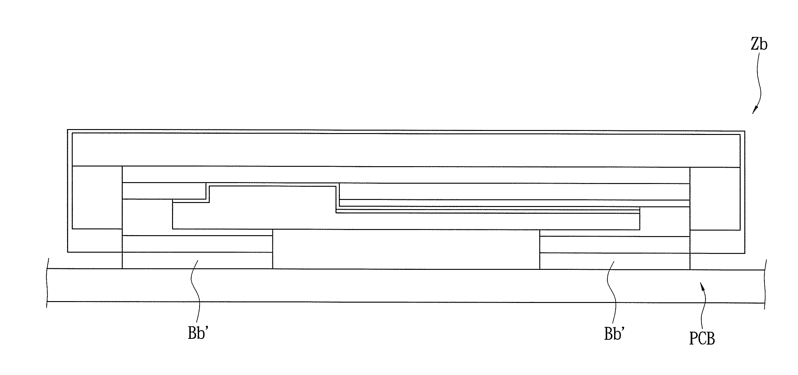
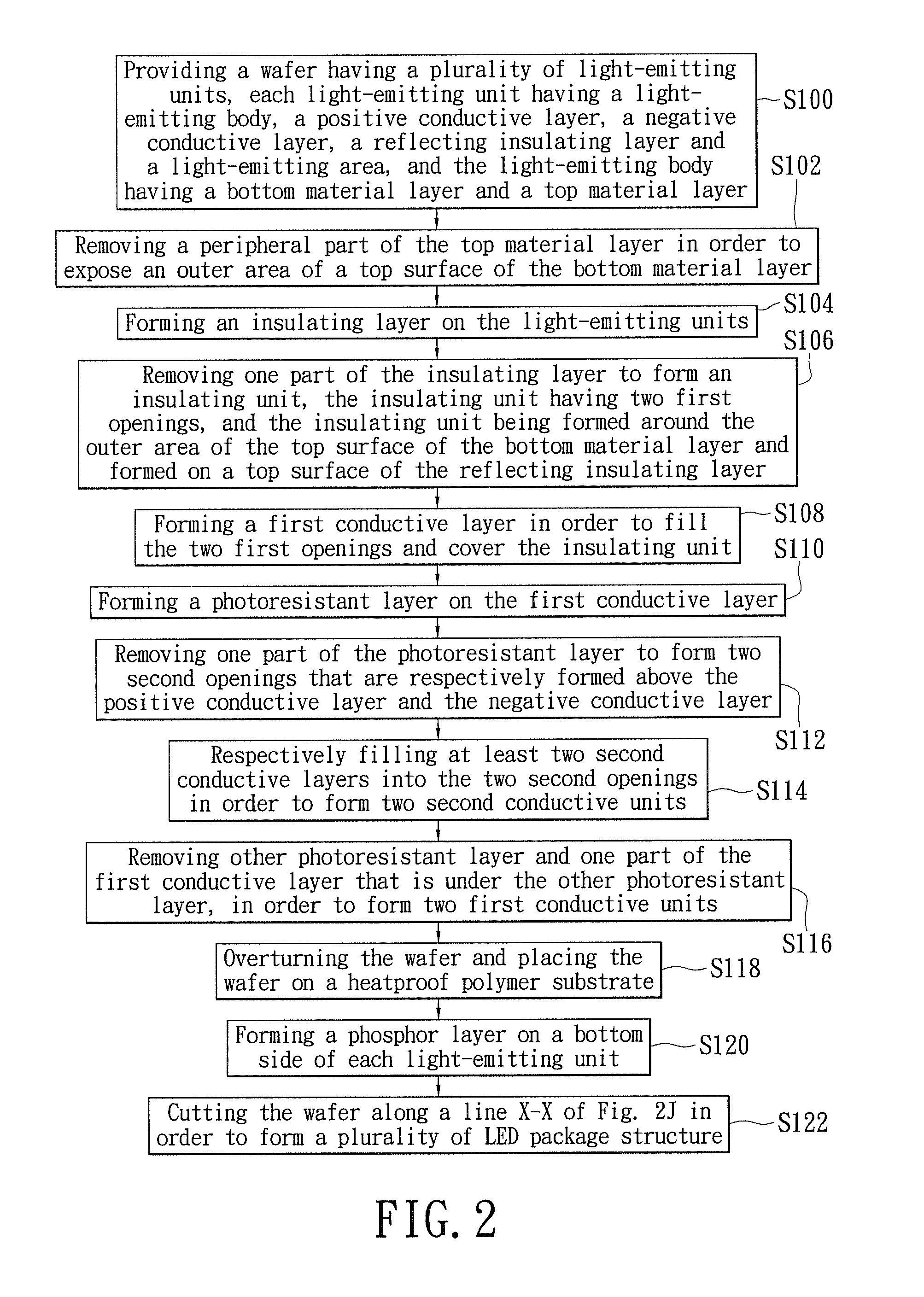
Wafer level LED package structure for increase light-emitting efficiency and method for making the same
PatentInactiveUS20120009699A1
Innovation
- A wafer level LED package structure is developed with an insulating unit to increase the thickness of the reflecting insulating layer, preventing short circuits between the positive and negative conductive layers, and including conductive units to ensure proper electrical connections.

Light-emitting element manufacturing method using wafer level package process and light-emitting element manufactured by same
PatentWO2016010378A1
Innovation
- A method involving a lens unit with grooves for forming a wavelength conversion unit, where the wavelength conversion characteristics are adjusted based on optical properties, ensuring uniform coverage on the side surfaces of nitride-based semiconductor structures, and the inclusion of a reflective layer and heat dissipation pad to enhance light extraction efficiency and reliability.


Manufacturing Standards for Wafer-Level Optics
The manufacturing of wafer-level optics for LED systems requires adherence to stringent standards that ensure optimal light efficiency and consistent performance across large-scale production. Current industry standards primarily follow ISO 14999 series for ophthalmic optics and ISO 10110 for optical elements, though these require adaptation for wafer-level manufacturing processes. The semiconductor industry's established SEMI standards provide foundational guidelines for wafer handling, cleanliness protocols, and dimensional tolerances that directly impact optical performance.
Surface quality specifications represent a critical manufacturing standard, with surface roughness typically maintained below 10 nanometers RMS to minimize scattering losses. The industry has adopted modified Scratch-Dig specifications, originally designed for conventional optics, with enhanced requirements for wafer-level applications. Surface defect density standards limit particulate contamination to less than 0.1 defects per square centimeter for particles exceeding 0.5 micrometers, ensuring minimal light obstruction and maintaining high transmission efficiency.
Dimensional accuracy standards for wafer-level optics demand tolerances significantly tighter than traditional semiconductor devices. Thickness uniformity across 200mm wafers must be maintained within ±2 micrometers, while surface figure accuracy requires deviations less than λ/4 at 587.6nm wavelength. These specifications ensure consistent focal properties and light distribution patterns across all optical elements manufactured on a single wafer.
Material purity and optical property standards govern the selection and processing of substrates and coating materials. Transmission requirements typically specify greater than 95% transmission in the visible spectrum, with absorption coefficients below 0.01 cm⁻¹. Refractive index uniformity must be maintained within ±0.0005 across the wafer surface to prevent optical aberrations that could reduce LED system efficiency.
Process control standards encompass environmental conditions, equipment calibration protocols, and quality assurance procedures. Clean room classifications follow ISO 14644 standards, typically requiring Class 100 or better environments during critical processing steps. Temperature control during manufacturing processes must be maintained within ±1°C to ensure consistent material properties and dimensional stability throughout the production cycle.
Thermal Management in High-Efficiency LED Systems
Thermal management represents one of the most critical challenges in achieving maximum light efficiency for wafer-level LED systems. As LED power densities continue to increase, the generation of waste heat becomes a primary limiting factor that directly impacts both luminous efficacy and device longevity. The fundamental relationship between junction temperature and light output efficiency creates a cascading effect where inadequate thermal control leads to reduced photon generation, spectral shifts, and accelerated degradation of semiconductor materials.
The physics of thermal generation in LED systems stems from the non-radiative recombination processes within the active region, where electrical energy converts to heat rather than photons. In high-efficiency wafer-level configurations, this thermal load becomes concentrated across densely packed arrays, creating localized hot spots that can exceed critical temperature thresholds. The resulting thermal resistance pathway from junction to ambient environment determines the overall system performance ceiling.
Advanced thermal interface materials have emerged as key enablers for wafer-level LED thermal management. These materials, including graphene-enhanced composites and phase-change thermal compounds, provide improved thermal conductivity while maintaining mechanical compliance necessary for wafer-level processing. The integration of these materials requires careful consideration of coefficient of thermal expansion matching to prevent stress-induced failures during thermal cycling.
Micro-channel cooling architectures represent a significant advancement in addressing thermal challenges at the wafer level. These systems utilize precisely etched cooling channels integrated directly into the substrate, enabling localized heat extraction with minimal thermal resistance. The implementation of such systems requires sophisticated fluid dynamics modeling to optimize flow distribution and prevent thermal gradients across the LED array.
Substrate material selection plays a crucial role in thermal management effectiveness. Silicon carbide and aluminum nitride substrates offer superior thermal conductivity compared to traditional sapphire substrates, enabling more efficient heat spreading from individual LED elements. The trade-offs between thermal performance, cost, and manufacturing compatibility continue to drive material innovation in this space.
Thermal modeling and simulation tools have become indispensable for optimizing wafer-level LED thermal designs. Finite element analysis coupled with computational fluid dynamics enables prediction of temperature distributions and identification of thermal bottlenecks before physical prototyping. These tools facilitate the optimization of heat sink geometries, thermal via placement, and cooling system configurations to maximize overall light efficiency while maintaining acceptable operating temperatures.
Unlock deeper insights with Patsnap Eureka Quick Research — get a full tech report to explore trends and direct your research. Try now!
Generate Your Research Report Instantly with AI Agent
Supercharge your innovation with Patsnap Eureka AI Agent Platform!