

Memristor-Based Integrated Circuit Developments: Apply Here
APR 17, 20269 MIN READ
Generate Your Research Report Instantly with AI Agent
PatSnap Eureka helps you evaluate technical feasibility & market potential.
Memristor Technology Background and Development Goals
Memristor technology represents a revolutionary advancement in non-volatile memory and neuromorphic computing, emerging from the theoretical foundation laid by Leon Chua in 1971. This fourth fundamental passive circuit element, characterized by its ability to retain resistance states without power, has evolved from a mathematical concept to a tangible technology with profound implications for integrated circuit development. The memristor's unique property of "remembering" its resistance history positions it as a cornerstone technology for next-generation computing architectures.
The historical trajectory of memristor development spans over five decades, beginning with Chua's theoretical prediction and reaching a pivotal milestone in 2008 when HP Labs demonstrated the first practical memristor device. This breakthrough validated decades of theoretical work and sparked intensive research across academia and industry. The technology has since progressed through multiple phases, from basic material science investigations to sophisticated device engineering and system-level integration studies.
Current development trends indicate a convergence toward practical applications in artificial intelligence, edge computing, and ultra-low-power systems. The technology's evolution reflects a shift from proof-of-concept demonstrations to commercially viable solutions, driven by the increasing demand for energy-efficient computing paradigms and the limitations of traditional von Neumann architectures in handling data-intensive applications.
The primary technological objectives encompass several critical domains. Foremost among these is achieving reliable, high-density memory arrays that can compete with or surpass existing non-volatile memory technologies in terms of speed, endurance, and retention characteristics. The target specifications include switching speeds in the nanosecond range, endurance exceeding 10^12 cycles, and retention periods spanning decades under operational conditions.
Neuromorphic computing applications represent another fundamental goal, where memristors serve as artificial synapses in brain-inspired computing architectures. The objective involves developing devices capable of mimicking biological neural networks' plasticity and learning mechanisms, enabling real-time adaptation and pattern recognition capabilities. This requires precise control over conductance modulation and the ability to implement various learning algorithms at the hardware level.
Integration challenges form a critical aspect of current development goals, particularly regarding CMOS compatibility and scalability to advanced technology nodes. The objectives include developing fabrication processes that seamlessly integrate with existing semiconductor manufacturing infrastructure while maintaining device performance and reliability standards. Additionally, achieving three-dimensional integration capabilities represents a key milestone for maximizing storage density and computational throughput in future integrated circuits.
Market Demand for Memristor-Based IC Applications
The global semiconductor industry is experiencing unprecedented demand for next-generation memory and computing solutions, driven by the exponential growth of data-intensive applications and the limitations of traditional silicon-based technologies. Memristor-based integrated circuits have emerged as a compelling solution to address critical market needs across multiple sectors, positioning themselves at the intersection of memory storage, neuromorphic computing, and edge processing applications.
Data centers and cloud computing infrastructure represent the largest addressable market for memristor-based ICs, where the technology's non-volatile characteristics and high-density storage capabilities directly address the growing demand for energy-efficient memory solutions. The persistent nature of memristors eliminates the need for constant power refresh cycles, significantly reducing operational costs in large-scale computing environments. Major cloud service providers are actively seeking alternatives to conventional DRAM and NAND flash technologies to overcome the memory wall bottleneck that constrains system performance.
The artificial intelligence and machine learning sector demonstrates substantial market pull for memristor technology, particularly in neuromorphic computing applications. The inherent analog computing capabilities of memristors enable direct implementation of synaptic functions, making them ideal for edge AI devices where power efficiency and real-time processing are critical requirements. Mobile device manufacturers and autonomous vehicle developers are driving demand for low-power, high-performance computing solutions that can execute complex neural network algorithms locally.
Internet of Things applications create another significant market opportunity, where memristor-based ICs can provide ultra-low power memory solutions for sensor networks and embedded systems. The technology's ability to retain data without power makes it particularly valuable for battery-operated devices that require long operational lifespans with minimal maintenance. Industrial IoT deployments in harsh environments benefit from memristors' inherent radiation tolerance and temperature stability.
The automotive electronics market is increasingly demanding robust, high-reliability memory solutions for advanced driver assistance systems and autonomous driving platforms. Memristor technology addresses the stringent automotive qualification requirements while providing the high-speed data processing capabilities necessary for real-time decision making in safety-critical applications.
Emerging applications in quantum computing interfaces and photonic integrated circuits are creating niche but high-value market segments where memristors serve as crucial interface components between classical and quantum systems, further expanding the technology's market potential across diverse application domains.
Current State and Challenges of Memristor Integration
Memristor technology has achieved significant milestones in laboratory demonstrations, with successful fabrication of devices exhibiting stable resistance switching behaviors. Leading research institutions have demonstrated memristor arrays with switching speeds in the nanosecond range and endurance cycles exceeding 10^12 operations. Current fabrication processes primarily utilize titanium dioxide, hafnium oxide, and tantalum oxide materials, with device dimensions scaling down to sub-10 nanometer nodes.
However, several critical challenges impede widespread commercial adoption. Device-to-device variability remains a primary concern, with resistance values showing significant statistical variations across large arrays. This variability stems from atomic-scale defect distributions and interface irregularities that are difficult to control during manufacturing processes. Cycle-to-cycle variations also affect reliability, as resistance states can drift over time due to structural changes in the switching medium.
Thermal stability presents another substantial obstacle, particularly in high-density integration scenarios. Memristors exhibit temperature-dependent switching characteristics, and thermal crosstalk between adjacent devices can cause unintended state changes. The sneak path problem in crossbar architectures further complicates integration, where current flows through unselected devices, leading to power consumption issues and potential data corruption.
Manufacturing scalability poses significant economic challenges. Current fabrication techniques require precise control of material deposition and interface engineering, resulting in low yields and high production costs. The integration of memristors with conventional CMOS processes demands specialized equipment and process modifications, increasing overall manufacturing complexity.
Standardization efforts are still in early stages, with limited industry consensus on device specifications, testing protocols, and reliability metrics. This lack of standardization hampers technology transfer from research laboratories to commercial production lines. Additionally, the absence of mature design automation tools and circuit simulation models creates barriers for system-level integration and product development.
Despite these challenges, recent advances in atomic layer deposition techniques and improved understanding of switching mechanisms have enhanced device uniformity. Emerging selector device technologies and novel circuit architectures show promise in addressing sneak path issues and improving array performance, indicating potential pathways toward commercial viability.
Current Memristor Integration Technical Solutions
01 Memristor crossbar array architectures for memory and computing
Memristor-based integrated circuits utilize crossbar array architectures where memristive elements are arranged in a grid pattern with intersecting conductive lines. These architectures enable high-density memory storage and in-memory computing capabilities. The crossbar configuration allows for efficient data storage and retrieval, as well as parallel processing operations. This architecture is particularly suitable for neuromorphic computing and analog computation applications where multiple memristive devices can be accessed simultaneously.- Memristor crossbar array architectures for memory and computing: Memristor-based integrated circuits can utilize crossbar array architectures where memristors are arranged in a grid pattern at the intersections of perpendicular conductive lines. This configuration enables high-density memory storage and in-memory computing capabilities. The crossbar structure allows for efficient data storage and retrieval, as well as performing computational operations directly within the memory array, reducing the need for data transfer between separate memory and processing units.
- Hybrid CMOS-memristor circuit integration: Integration of memristors with conventional CMOS technology enables the creation of hybrid circuits that combine the advantages of both technologies. This approach allows memristors to be incorporated into existing semiconductor manufacturing processes and integrated with traditional transistor-based circuits. The hybrid architecture can leverage CMOS circuits for control and signal processing while utilizing memristors for non-volatile storage and neuromorphic computing functions, creating versatile integrated circuit designs.
- Neuromorphic computing circuits using memristors: Memristor-based integrated circuits can be designed to emulate biological neural networks for neuromorphic computing applications. These circuits exploit the analog resistance states and synaptic-like behavior of memristors to implement artificial neurons and synapses. The memristor's ability to retain resistance states enables learning and pattern recognition capabilities, making them suitable for artificial intelligence and machine learning applications with low power consumption and high parallelism.
- Programming and control circuits for memristor devices: Specialized programming and control circuits are essential for operating memristor-based integrated circuits effectively. These circuits manage the voltage and current conditions required to switch memristors between different resistance states, ensuring reliable write and read operations. The control circuitry includes pulse generation, voltage regulation, and sensing mechanisms that enable precise manipulation of memristor states while preventing device degradation and ensuring long-term reliability.
- Multi-level cell memristor memory architectures: Advanced memristor-based memory circuits can store multiple bits per cell by utilizing multiple distinct resistance states. This multi-level cell approach increases storage density beyond binary memory systems. The integrated circuits incorporate sophisticated sensing and programming schemes to accurately distinguish between different resistance levels and maintain data integrity. This technology enables higher capacity memory systems while maintaining the non-volatile characteristics and fast switching speeds of memristor devices.
02 Memristor-based neuromorphic and artificial neural network circuits
Integrated circuits incorporating memristors can implement artificial neural networks and neuromorphic computing systems. Memristive devices serve as synaptic elements that can store and update weights in neural network architectures. These circuits enable hardware implementation of machine learning algorithms with low power consumption and high parallelism. The analog nature of memristors allows for efficient emulation of biological neural processes, including learning and adaptation mechanisms.Expand Specific Solutions03 Hybrid CMOS-memristor integrated circuit designs
Hybrid integrated circuits combine conventional CMOS transistor technology with memristive elements to leverage the advantages of both technologies. These designs integrate memristors with standard logic circuits, enabling enhanced functionality such as non-volatile memory integrated with processing units. The hybrid approach allows for compatibility with existing semiconductor manufacturing processes while adding memristor-specific capabilities. Such circuits can achieve improved performance in terms of power efficiency and computational density.Expand Specific Solutions04 Memristor programming and control circuits
Specialized control and programming circuits are essential for operating memristor-based integrated circuits. These circuits manage the voltage and current conditions required to switch memristive states and maintain desired resistance values. Programming circuits include pulse generation systems, voltage regulators, and feedback mechanisms to ensure accurate and reliable memristor operation. Advanced control schemes enable multi-level storage and precise analog tuning of memristive elements for various applications.Expand Specific Solutions05 Memristor-based logic and computational circuits
Memristors can be configured to perform logic operations and computational functions directly within the memory array. These circuits implement Boolean logic gates and arithmetic operations using the switching characteristics of memristive devices. Stateful logic approaches utilize the memory properties of memristors to perform computations without separate processing units. This integration of memory and logic enables novel computing paradigms with reduced data movement and improved energy efficiency for specific computational tasks.Expand Specific Solutions
Key Players in Memristor IC Industry Analysis
The memristor-based integrated circuit development landscape represents an emerging technology sector in its early commercialization phase, with significant growth potential driven by applications in neuromorphic computing and non-volatile memory systems. The market remains relatively nascent but shows promising expansion as demand for energy-efficient computing solutions increases. Technology maturity varies significantly across players, with established semiconductor companies like Advanced Micro Devices, Micron Technology, and Hewlett Packard Enterprise leading commercial development efforts, while academic institutions including Huazhong University of Science & Technology, University of Electronic Science & Technology of China, and Northwestern University drive fundamental research breakthroughs. Industrial players such as TDK Corp., DENSO Corp., and Tower Semiconductor are advancing manufacturing capabilities, creating a competitive ecosystem where traditional memory manufacturers compete alongside specialized research institutions to establish memristor technology as a viable alternative to conventional silicon-based circuits.
Hewlett Packard Enterprise Development LP
Technical Solution: HPE has developed memristor-based crossbar arrays for neuromorphic computing applications, implementing synaptic plasticity mechanisms that enable real-time learning capabilities. Their memristor technology utilizes titanium dioxide thin films with programmable resistance states, achieving switching speeds in the nanosecond range and endurance cycles exceeding 10^6 operations. The company has integrated these memristors into hybrid CMOS-memristor circuits for pattern recognition and associative memory applications, demonstrating energy efficiency improvements of up to 1000x compared to traditional digital implementations.
Advantages: Pioneer in memristor research with extensive patent portfolio and proven scalability. Disadvantages: Limited commercial deployment and high manufacturing complexity.
Advanced Micro Devices, Inc.
Technical Solution: AMD has explored memristor integration in processor architectures for in-memory computing applications, focusing on accelerating machine learning workloads. Their research involves embedding memristor crossbars within CPU cache hierarchies to perform matrix-vector multiplications directly in memory, reducing data movement overhead. The memristor-enhanced processors target AI inference applications where traditional von Neumann architectures create bottlenecks. AMD's approach combines CMOS logic with resistive switching devices to create hybrid computing units capable of both storage and computation functions.
Advantages: Strong processor design expertise and established semiconductor ecosystem partnerships. Disadvantages: Early-stage development with limited commercial products and integration complexity.
Core Patents in Memristor IC Technologies
Memristor-based circuit and method
PatentActiveUS20220329254A1
Innovation
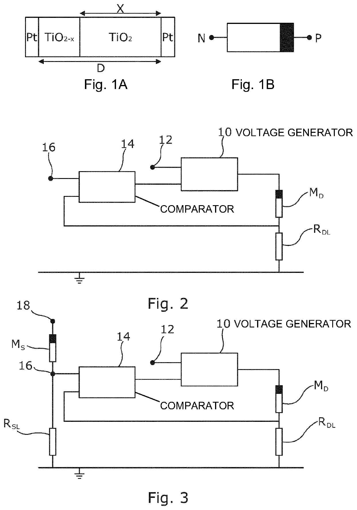
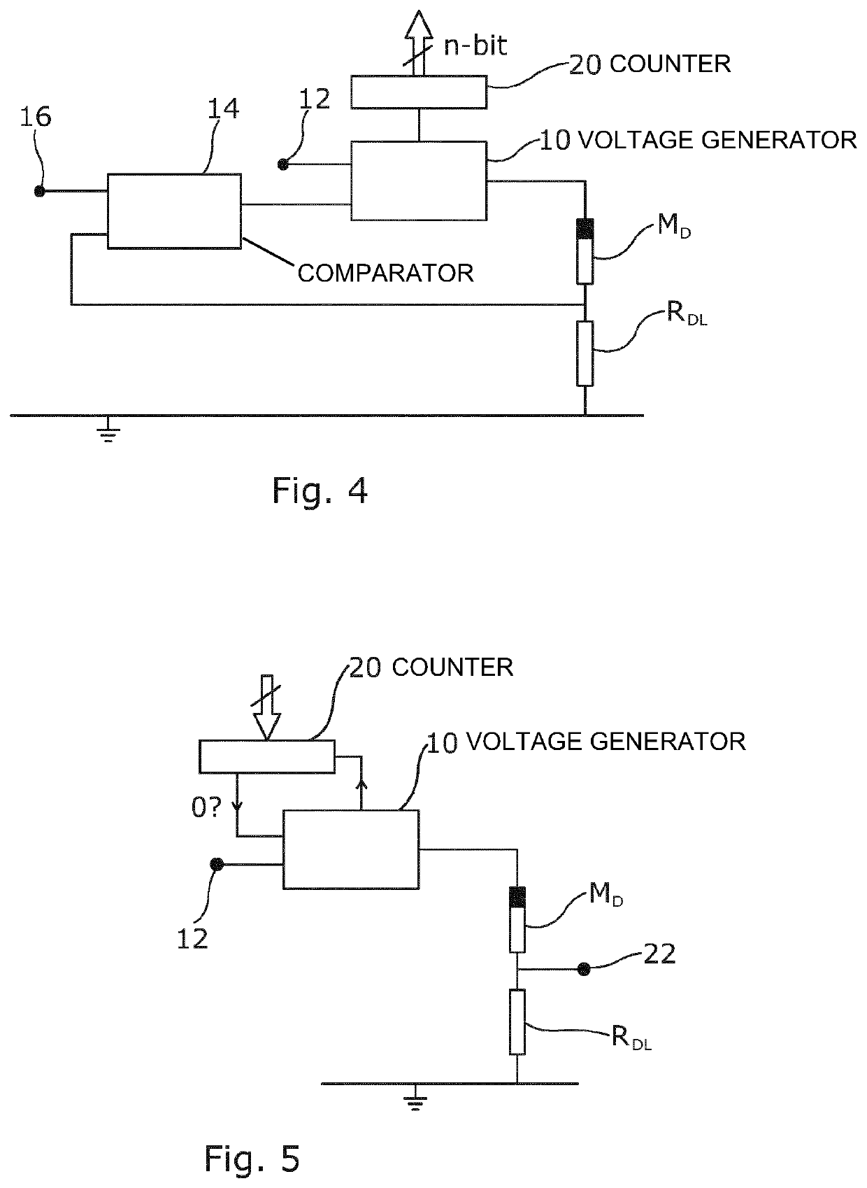
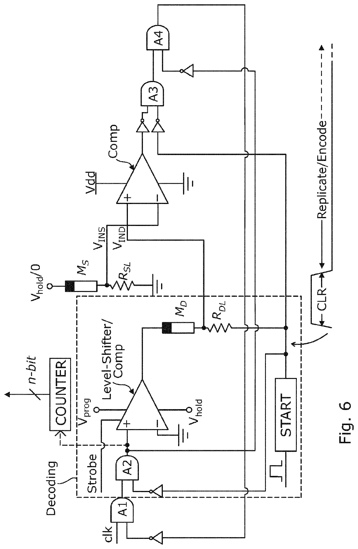
- A memristor-based circuit comprising a voltage generator that applies series of voltage pulses to incrementally change the memristor resistance, a comparator to ensure defined conditions are met, and a counter to track pulse numbers, enabling efficient replication, encoding, decoding, and authentication.

Memristor-protection integrated circuit and method for protection of a memristor during switching
PatentInactiveUS8111494B2
Innovation
- A memristor-protection integrated circuit (IC) is developed, incorporating a first and second current-bias circuit, an inverter, and a current limiter, which are configured to couple with memristors and limit current flow, preventing over-current conditions and protecting the memristors from damage during switching.


Manufacturing Standards for Memristor Devices
The establishment of comprehensive manufacturing standards for memristor devices represents a critical milestone in transitioning this revolutionary technology from laboratory prototypes to commercial-scale production. Current standardization efforts focus on defining precise material specifications, fabrication tolerances, and quality control metrics that ensure consistent device performance across different manufacturing facilities and production batches.
Material purity requirements constitute the foundation of memristor manufacturing standards, with specifications demanding ultra-high purity switching materials such as titanium dioxide, hafnium oxide, and tantalum oxide. These standards typically require impurity levels below 10 parts per million for critical dopants, as even trace contamination can significantly alter switching characteristics and device reliability. Additionally, electrode materials must meet stringent conductivity and adhesion requirements to prevent interface degradation during operation.
Dimensional tolerances represent another crucial aspect of manufacturing standards, particularly given the nanoscale nature of memristor devices. Current industry guidelines specify thickness variations of less than ±2% for switching layers, typically ranging from 5 to 50 nanometers. Lateral dimensions must maintain precision within ±10 nanometers to ensure consistent switching voltages and current levels across device arrays.
Process control standards encompass critical fabrication parameters including deposition temperatures, annealing conditions, and ambient atmosphere requirements. These specifications mandate controlled environments with oxygen and moisture levels below specific thresholds, typically requiring cleanroom facilities with Class 10 or better contamination control. Temperature uniformity across wafer surfaces must remain within ±2°C during critical processing steps.
Quality assurance protocols define comprehensive testing procedures for evaluating device performance metrics including switching speed, endurance cycles, retention characteristics, and variability parameters. These standards require statistical sampling methods with minimum sample sizes and acceptance criteria based on normal distribution parameters. Electrical characterization must demonstrate switching ratios exceeding 100:1 and endurance capabilities surpassing 10^9 cycles for commercial applications.
Packaging and integration standards address the unique challenges of incorporating memristor devices into conventional semiconductor manufacturing flows. These specifications define compatible process temperatures, chemical compatibility requirements, and mechanical stress limitations to prevent device degradation during subsequent processing steps. Standardized interface protocols ensure seamless integration with existing CMOS technologies while maintaining device functionality and reliability throughout the complete manufacturing sequence.
Intellectual Property Landscape in Memristor Field
The intellectual property landscape in the memristor field represents a complex and rapidly evolving ecosystem characterized by intense patent activity and strategic positioning among major technology players. Patent filings in memristor technology have experienced exponential growth since 2008, with over 3,000 patent families filed globally as of 2024. The distribution reveals a concentration of intellectual property assets primarily held by semiconductor giants, research institutions, and emerging startups specializing in neuromorphic computing applications.
Geographic analysis of patent ownership demonstrates clear regional clusters, with the United States leading in fundamental memristor patents, accounting for approximately 40% of global filings. South Korea follows closely with 25%, driven primarily by Samsung and SK Hynix investments in memory applications. China represents 20% of patents, focusing heavily on manufacturing processes and materials science innovations. European patents constitute 12%, with Germany and the Netherlands contributing significantly through IMEC and Infineon research initiatives.
The patent landscape exhibits distinct technological domains within memristor development. Memory applications dominate with 45% of patents, covering resistive random-access memory (ReRAM) implementations and storage architectures. Neuromorphic computing patents represent 30% of filings, emphasizing synaptic devices and brain-inspired computing systems. Logic circuit applications account for 15%, while sensing and analog computing patents comprise the remaining 10%.
Key patent holders have established comprehensive intellectual property portfolios spanning multiple technological layers. IBM leads in fundamental device physics patents, while Intel focuses on integration and manufacturing scalability. Hewlett Packard Enterprise maintains strong positions in crossbar architectures and hybrid computing systems. Asian companies like Samsung and TSMC concentrate on process technology and yield optimization patents.
The competitive dynamics reveal strategic patent clustering around critical bottlenecks, particularly in materials engineering, device reliability, and large-scale integration challenges. Cross-licensing agreements have become increasingly common, indicating industry recognition of the interdependent nature of memristor technology development and the necessity for collaborative approaches to overcome fundamental technical barriers.
Unlock deeper insights with PatSnap Eureka Quick Research — get a full tech report to explore trends and direct your research. Try now!
Generate Your Research Report Instantly with AI Agent
Supercharge your innovation with PatSnap Eureka AI Agent Platform!