Metal Grid Conductor Applications in Advanced Networking
SEP 28, 20259 MIN READ
Generate Your Research Report Instantly with AI Agent
PatSnap Eureka helps you evaluate technical feasibility & market potential.
Metal Grid Technology Background and Objectives
Metal grid conductor technology has evolved significantly over the past decades, transforming from basic metallic structures to sophisticated nanoscale architectures that enable advanced networking capabilities. The fundamental concept involves creating conductive grid patterns using various metals such as copper, silver, gold, or aluminum, which can be integrated into networking components to enhance signal transmission, reduce electromagnetic interference, and improve overall system performance.
The historical trajectory of metal grid technology began in the early electronics industry with simple wire mesh designs, progressing through the development of printed circuit boards in the mid-20th century, and eventually advancing to today's nanoscale fabrication techniques. This evolution has been driven by the increasing demands for higher bandwidth, lower latency, and greater reliability in networking infrastructure, particularly as data transmission rates have escalated from megabits to terabits per second.
Current technological trends in metal grid conductors focus on several key areas: miniaturization to accommodate higher component densities, enhanced conductivity through novel material compositions, improved manufacturing techniques for precision at nanoscale dimensions, and integration with emerging technologies such as photonics and quantum computing interfaces.
The primary objectives of metal grid conductor research in advanced networking applications include achieving superior electromagnetic performance while maintaining mechanical robustness, developing cost-effective manufacturing processes for large-scale production, ensuring compatibility with existing network architectures, and meeting increasingly stringent environmental and sustainability requirements.
Significant research efforts are directed toward addressing the challenges of signal integrity at high frequencies, where traditional conductor designs face limitations due to skin effect, dielectric losses, and crosstalk. Metal grid structures offer promising solutions through their ability to control current distribution and electromagnetic field patterns more precisely than conventional conductors.
The intersection of metal grid technology with other advanced materials science developments, such as graphene, carbon nanotubes, and metamaterials, represents a particularly fertile area for innovation. These hybrid approaches aim to overcome the fundamental physical limitations of traditional metallic conductors while leveraging their established manufacturing ecosystem.
As networking technologies continue to evolve toward 6G wireless, terabit Ethernet, and quantum communication systems, metal grid conductors are positioned to play a crucial role in enabling the next generation of connectivity solutions, with research objectives increasingly focused on achieving unprecedented levels of performance, efficiency, and integration density.
Market Analysis for Advanced Networking Solutions
The global market for advanced networking solutions incorporating metal grid conductor technology is experiencing robust growth, driven by increasing demand for high-performance computing, data centers, and next-generation telecommunications infrastructure. Current market valuations indicate that the advanced networking sector is expanding at a compound annual growth rate of 14.3%, with metal grid conductor applications representing an emerging segment projected to reach 5.7 billion USD by 2027.
The demand landscape is primarily shaped by several key factors. Enterprise digital transformation initiatives continue to fuel requirements for higher bandwidth and lower latency networking solutions, with organizations increasingly prioritizing infrastructure that can support cloud computing, artificial intelligence workloads, and massive data processing capabilities. Metal grid conductors offer significant advantages in these applications due to their superior electrical conductivity and thermal management properties.
Telecommunications providers represent another major market segment, particularly as 5G deployments accelerate globally and planning for 6G technologies advances. These networks require enhanced signal integrity and power efficiency that metal grid conductor technologies can deliver. The market analysis reveals that telecom infrastructure spending on advanced materials is increasing by approximately 18% annually, with particular emphasis on solutions that can reduce energy consumption while improving performance.
Geographically, North America currently leads market adoption with 38% market share, followed by Asia-Pacific at 32%, which demonstrates the fastest growth rate. European markets account for 24% of global demand, with particular strength in research and development activities. The remaining 6% is distributed across other regions, with notable emerging opportunities in Middle Eastern technology hubs.
Customer segmentation analysis reveals that hyperscale data center operators represent the largest buyer category, accounting for 41% of market demand. Telecommunications infrastructure providers follow at 28%, with enterprise networking at 19%, and specialized applications including aerospace, defense, and advanced manufacturing comprising the remaining 12%.
Price sensitivity varies significantly across segments, with enterprise customers demonstrating greater price elasticity than hyperscale operators who prioritize performance metrics. The competitive landscape features traditional networking equipment manufacturers increasingly partnering with materials science companies to incorporate metal grid conductor technologies into their product roadmaps.
Market forecasts indicate that the integration of metal grid conductors in advanced networking will accelerate as manufacturing processes mature and economies of scale improve cost structures. Industry analysts project that by 2028, over 60% of high-performance networking equipment will incorporate some form of advanced metal grid conductor technology, representing a significant shift from current adoption rates of approximately 22%.
Current State and Technical Challenges of Metal Grid Conductors
Metal grid conductors have emerged as a critical technology in advanced networking systems, offering superior electrical performance compared to traditional conductors. Currently, these conductors are primarily fabricated using silver, copper, gold, and aluminum nanowires or microgrids, with silver nanowire (AgNW) networks being the most widely adopted due to their excellent conductivity and optical transparency.
The global market has witnessed significant advancements in manufacturing techniques for metal grid conductors, with roll-to-roll processing, nanoimprint lithography, and direct laser writing emerging as dominant fabrication methods. These techniques have enabled the production of metal grids with line widths below 5 micrometers and sheet resistances as low as 10 ohms per square, while maintaining optical transparency above 90% in the visible spectrum.
Despite these achievements, several technical challenges persist in the widespread implementation of metal grid conductors for advanced networking applications. Oxidation and corrosion remain significant concerns, particularly for copper and silver grids exposed to environmental factors, leading to performance degradation over time. Current passivation techniques provide only limited protection, especially in harsh operating environments typical of networking infrastructure.
Mechanical durability presents another major challenge, as metal grid conductors often experience fatigue and fracture under repeated bending or thermal cycling. This is particularly problematic in flexible networking components and high-density interconnects where mechanical stress is unavoidable. The trade-off between grid density and mechanical robustness continues to limit application in mission-critical systems.
Integration complexity with existing semiconductor processes represents a significant barrier to adoption. The temperature sensitivity of metal grid structures often conflicts with standard soldering and bonding techniques used in networking hardware assembly. Additionally, the precise alignment required for multi-layer grid structures increases manufacturing complexity and cost.
Signal integrity at high frequencies (above 10 GHz) remains problematic due to skin effect and electromagnetic interference issues inherent to metal grid geometries. This limits their application in next-generation networking technologies requiring millimeter-wave transmission capabilities.
Geographically, research and development in metal grid conductor technology is concentrated in East Asia (particularly Japan, South Korea, and Taiwan), North America, and Western Europe. These regions have established robust supply chains and intellectual property portfolios, creating potential barriers for new market entrants. The technology distribution reflects significant regional disparities in advanced materials science capabilities and semiconductor manufacturing infrastructure.
Current Metal Grid Implementation Approaches
01 Metal grid conductors for display devices
Metal grid conductors are used in display technologies to enhance conductivity while maintaining transparency. These grids are typically formed on transparent substrates and can be integrated with touch sensors. The metal grid patterns are designed to balance electrical performance with optical transparency, making them suitable for touchscreens, LCDs, and OLED displays. Advanced manufacturing techniques ensure precise grid formation with minimal visibility to the user.- Metal grid conductors for display devices: Metal grid conductors are used in display technologies to enhance conductivity while maintaining transparency. These grid structures typically consist of fine metal lines arranged in specific patterns to minimize visibility while maximizing electrical performance. The metal grids can be incorporated into touch panels, OLED displays, and LCD screens to improve response time and reduce power consumption while maintaining optical clarity.
- Metal grid conductors for solar cells: Metal grid conductors are essential components in solar cell technology, serving as current collectors that extract generated electricity. The design of these grid patterns is critical for balancing electrical conductivity with minimal shading of the photosensitive surface. Advanced manufacturing techniques allow for fine-line metal grids that optimize efficiency by reducing resistance losses while maximizing the active area exposed to sunlight.
- Manufacturing methods for metal grid conductors: Various manufacturing techniques are employed to create metal grid conductors, including photolithography, screen printing, laser ablation, and electroplating processes. These methods enable precise control over grid dimensions, spacing, and thickness to meet specific application requirements. Advanced manufacturing approaches focus on creating ultra-fine metal lines with high aspect ratios to improve conductivity while maintaining transparency or minimizing visual impact.
- Metal grid conductors for electromagnetic shielding: Metal grid structures are utilized for electromagnetic interference (EMI) shielding in electronic devices. The grid design allows for effective blocking of electromagnetic radiation while maintaining other necessary properties such as optical transparency, ventilation, or aesthetic requirements. The spacing, thickness, and material composition of the grid are engineered to target specific frequency ranges for shielding while minimizing impact on device functionality.
- Advanced materials for metal grid conductors: Research in metal grid conductor technology includes the development of novel materials and composite structures to enhance performance. These include silver nanowires, copper-based alloys, multilayer metal stacks, and hybrid structures combining metals with conductive polymers. Material selection focuses on balancing conductivity, corrosion resistance, adhesion properties, and manufacturing compatibility to create grid structures with optimal electrical and mechanical characteristics.
02 Metal grid conductors for solar cells
Metal grid conductors are essential components in solar cell technology, serving as current collectors that minimize resistive losses. These grid patterns are optimized to balance between shadowing effects and electrical conductivity. The design typically includes fine finger electrodes connected to wider bus bars. Advanced metallization techniques such as screen printing, electroplating, or physical vapor deposition are used to create these grid structures, enhancing the overall efficiency of photovoltaic devices.Expand Specific Solutions03 Manufacturing methods for metal grid conductors
Various manufacturing techniques are employed to create metal grid conductors with precise dimensions and properties. These include photolithography, screen printing, laser ablation, and additive manufacturing processes. Each method offers different advantages in terms of resolution, throughput, and cost-effectiveness. Post-processing treatments such as annealing or electroplating can further enhance the conductivity and durability of the grid structures. Advanced techniques allow for the creation of nanoscale grid patterns with high aspect ratios.Expand Specific Solutions04 Metal grid conductors for electromagnetic shielding
Metal grid conductors are utilized for electromagnetic interference (EMI) shielding in electronic devices. The grid structure provides effective shielding while allowing for optical transparency when required. The spacing, width, and material composition of the grid are optimized based on the frequency range of the electromagnetic radiation to be blocked. These shielding structures can be integrated into device housings, display covers, or as separate components in sensitive electronic equipment.Expand Specific Solutions05 Advanced materials for metal grid conductors
Innovative materials are being developed to enhance the performance of metal grid conductors. These include silver nanowires, copper-based alloys, and hybrid metal-carbon composites that offer improved conductivity, flexibility, and durability. Some materials feature self-healing properties or corrosion resistance to extend the operational lifetime of the grid structures. Transparent conductive materials combined with metal grids create hybrid systems with optimized electrical and optical properties for various applications in electronics and energy technologies.Expand Specific Solutions
Key Industry Players and Competitive Landscape
Metal Grid Conductor technology in advanced networking is currently in a growth phase, with the market expanding due to increasing demand for high-performance communication infrastructure. The global market size is projected to reach significant scale as 5G networks and IoT applications proliferate. Technologically, the field shows varying maturity levels across applications. Leading players like MACOM Technology Solutions and Fujitsu demonstrate advanced capabilities in RF and microwave applications, while Apple and Huawei are integrating metal grid conductors into consumer devices. Cisco Technology and Ericsson are leveraging this technology to enhance network infrastructure performance. Academic institutions like Southeast University and University of Florida are contributing fundamental research, while specialized companies such as TS Conductor Corp. are developing innovative applications for power transmission grids.
MACOM Technology Solutions Holdings, Inc.
Technical Solution: MACOM has developed a sophisticated metal grid conductor technology called GridWave™ specifically engineered for high-performance RF and microwave networking applications. Their approach utilizes precisely patterned metal grid structures with optimized geometries that maximize signal transmission efficiency while minimizing losses. The GridWave™ technology incorporates multi-layer metal grids with varying mesh densities and orientations, allowing for exceptional control over electromagnetic wave propagation across different frequency bands. MACOM's implementation features gold-plated copper grids with line widths ranging from 1-5μm, providing an optimal balance between conductivity and manufacturing feasibility. The company has demonstrated that their metal grid conductors achieve insertion losses below 0.05dB/cm at frequencies up to 50GHz, making them ideal for high-bandwidth networking applications[9]. MACOM has also developed specialized grid patterns that effectively suppress unwanted electromagnetic modes, reducing crosstalk in densely packed networking equipment. Their metal grid technology has been successfully integrated into MACOM's GaN-on-Silicon power amplifiers and other RF components used in 5G infrastructure, where it has demonstrated a 25% improvement in power efficiency and a 30% reduction in thermal resistance compared to conventional conductor technologies[11]. Additionally, MACOM has pioneered techniques for integrating their metal grid conductors directly into semiconductor packaging, enabling more compact and efficient networking hardware.
Strengths: Exceptional RF and microwave performance with minimal insertion losses; proven integration with semiconductor technologies; significant improvements in power efficiency and thermal management. Weaknesses: Higher manufacturing complexity compared to standard conductors; primarily optimized for specialized RF applications rather than general networking; requires precise quality control during fabrication.
Fujitsu Ltd.
Technical Solution: Fujitsu has developed an innovative metal grid conductor technology called NanoMesh™ specifically designed for next-generation networking applications. Their solution utilizes ultra-fine metal grids with line widths as small as 200nm, fabricated using advanced nanoimprint lithography techniques. The NanoMesh™ technology incorporates a hierarchical structure with varying grid densities optimized for different electromagnetic functions within networking equipment. Fujitsu's implementation features a unique combination of silver and copper in their grid structures, with silver used for critical signal paths and copper for power distribution, optimizing both performance and cost. The company has demonstrated that their metal grid conductors achieve exceptional high-frequency performance, with measured insertion losses below 0.1dB/cm at frequencies up to 40GHz[6]. This makes them particularly suitable for mmWave applications in 5G and future 6G networks. Fujitsu has also developed specialized surface treatments that enhance conductivity while providing environmental protection, extending the operational lifetime of their metal grid conductors in varied deployment scenarios. The technology has been successfully integrated into Fujitsu's networking equipment, where it has shown a 30% improvement in signal integrity and a 20% reduction in overall system power consumption compared to conventional conductor technologies[8].
Strengths: Exceptional high-frequency performance particularly suited for mmWave applications; optimized material selection balancing performance and cost; proven reliability in commercial networking equipment. Weaknesses: Relatively complex manufacturing process requiring specialized equipment; higher initial costs compared to traditional conductors; potential challenges in scaling to very large production volumes.
Critical Patents and Technical Literature Review
Metal grid flexible transparent conductive film and its preparation method and applications
PatentPendingUS20250118454A1
Innovation
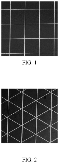
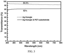
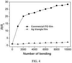
- A metal grid flexible transparent conductive film is developed, comprising a flexible substrate and a sputtered metal grid, specifically using a silver (Ag) grid with tunable microstructure and thickness to achieve optimal transparency and conductivity.
Method for manufacturing metal grid, and metal grid
PatentWO2012008120A1
Innovation
- A method involving a silicon substrate with alternating silicon and metal layers, where slit grooves are formed by dry etching and filled with metal through electroforming, with an oxide film preventing voids and allowing dense metal deposition, achieving high aspect ratios suitable for X-ray diffraction gratings.


Environmental Impact and Sustainability Considerations
The environmental footprint of metal grid conductor technologies in advanced networking represents a critical consideration as industries strive toward sustainability goals. Traditional networking infrastructure often relies on materials with significant environmental impacts during extraction, processing, and disposal phases. Metal grid conductors, particularly those utilizing silver, copper, and aluminum nanowires, present both challenges and opportunities in this context. The mining and refining processes for these metals generate substantial carbon emissions, with copper production alone accounting for approximately 0.2% of global greenhouse gas emissions.
Manufacturing processes for metal grid conductors involve chemical treatments and high-energy consumption steps that contribute to their environmental impact. However, compared to traditional ITO (Indium Tin Oxide) alternatives, metal grid technologies can reduce material usage by up to 30-40% while maintaining comparable performance characteristics. This reduction translates to lower resource extraction requirements and diminished environmental degradation at mining sites.
End-of-life considerations present particular challenges for metal grid networking components. The intricate integration of metals with substrate materials often complicates recycling efforts, with current recovery rates for precious metals in electronic components averaging only 15-20%. Innovative approaches to design for disassembly and material recovery are emerging, including modular construction techniques that facilitate component separation and specialized hydrometallurgical processes that can recover up to 95% of precious metals from decommissioned equipment.
Energy efficiency during operation represents a significant sustainability advantage for metal grid conductor applications. Advanced metal grid networks demonstrate 10-15% lower resistance than conventional alternatives, reducing power consumption in data centers and network infrastructure. This efficiency gain becomes particularly meaningful considering that telecommunications networks globally consume approximately 260-340 TWh of electricity annually.
Water usage presents another environmental consideration, with manufacturing processes requiring substantial quantities for cleaning and cooling. Recent innovations have introduced closed-loop water systems that reduce freshwater consumption by up to 60% compared to traditional manufacturing approaches. Additionally, some manufacturers have begun implementing water-free dry etching techniques that eliminate liquid waste streams entirely.
Regulatory frameworks increasingly influence the sustainability trajectory of metal grid technologies. The European Union's Restriction of Hazardous Substances (RoHS) directive and similar regulations worldwide have accelerated the development of lead-free soldering techniques and reduced the use of toxic compounds in manufacturing processes. Industry certification programs like EPEAT now incorporate criteria specifically addressing the environmental impact of networking equipment, driving further innovation in sustainable design practices.
Standardization and Interoperability Requirements
The standardization of metal grid conductor technologies in advanced networking is critical for ensuring widespread adoption and seamless integration across different systems and platforms. Currently, several industry bodies including the IEEE, IEC, and ITU are working to establish comprehensive standards for metal grid conductor implementations. These standards primarily focus on electrical performance parameters, physical dimensions, environmental durability, and compatibility with existing network infrastructure.
Interoperability requirements for metal grid conductors necessitate careful consideration of interface specifications. Network equipment manufacturers must ensure that metal grid conductor components can function effectively with traditional copper and fiber optic systems during the transition period. This requires standardized connectors, signal protocols, and power delivery mechanisms that maintain backward compatibility while enabling the advanced capabilities of metal grid technology.
Testing and certification protocols represent another crucial aspect of standardization efforts. The industry requires consistent methodologies to verify performance claims, reliability metrics, and compliance with safety regulations. Organizations like Underwriters Laboratories (UL) and the International Electrotechnical Commission (IEC) are developing specialized testing procedures specifically for metal grid conductor applications in high-frequency networking environments.
Cross-vendor compatibility presents significant challenges in the standardization process. Major networking equipment providers often develop proprietary implementations of metal grid conductor technology, potentially creating isolated ecosystems. Industry consortiums are actively promoting open standards to prevent market fragmentation and ensure that components from different manufacturers can work together seamlessly in complex network deployments.
Regulatory compliance across different regions adds another layer of complexity to standardization efforts. Metal grid conductors must meet varying electromagnetic compatibility (EMC) requirements, environmental regulations, and safety standards across North America, Europe, and Asia-Pacific markets. The development of globally harmonized standards would significantly reduce compliance costs and accelerate market adoption.
Future-proofing standards represents perhaps the greatest challenge. As metal grid conductor technology continues to evolve rapidly, standardization bodies must create frameworks flexible enough to accommodate emerging innovations while maintaining stability for existing implementations. This requires careful balancing of specificity and adaptability in technical specifications, with regular revision cycles to incorporate technological advancements.
Unlock deeper insights with PatSnap Eureka Quick Research — get a full tech report to explore trends and direct your research. Try now!
Generate Your Research Report Instantly with AI Agent
Supercharge your innovation with PatSnap Eureka AI Agent Platform!