

MOSFET vs BiCMOS: Integration into Complex Networks
APR 1, 20269 MIN READ
Generate Your Research Report Instantly with AI Agent
Patsnap Eureka helps you evaluate technical feasibility & market potential.
MOSFET vs BiCMOS Technology Background and Integration Goals
MOSFET (Metal-Oxide-Semiconductor Field-Effect Transistor) technology emerged in the 1960s as a revolutionary advancement in semiconductor design, fundamentally transforming the landscape of digital electronics. The technology's foundation lies in its ability to control current flow through voltage-controlled gates, enabling efficient switching operations with minimal power consumption. This characteristic made MOSFET the cornerstone of modern CMOS (Complementary Metal-Oxide-Semiconductor) technology, which dominates today's digital integrated circuits.
BiCMOS technology represents a sophisticated hybrid approach that combines the strengths of both bipolar junction transistors and CMOS devices on a single substrate. Developed in the 1980s, BiCMOS emerged from the recognition that while CMOS excelled in digital applications due to low power consumption and high integration density, bipolar transistors offered superior analog performance, higher current drive capability, and faster switching speeds for specific applications.
The evolution of both technologies has been driven by the relentless pursuit of Moore's Law, pushing toward smaller geometries, higher performance, and increased functionality. MOSFET technology has progressed through multiple generations, from micron-scale devices to today's sub-nanometer processes, incorporating innovations such as FinFET structures and high-k dielectrics to overcome physical limitations and maintain scaling momentum.
The integration challenge in complex networks stems from the diverse requirements of modern electronic systems. Contemporary applications demand simultaneous optimization of digital processing, analog signal conditioning, radio frequency communication, and power management functions. MOSFET technology excels in digital domains, offering exceptional scalability and power efficiency for processors, memory, and digital signal processing units.
BiCMOS technology addresses the limitations of pure CMOS implementations in mixed-signal environments. The bipolar components provide enhanced current drive capabilities essential for output buffers, analog amplifiers, and high-speed interfaces, while the CMOS portions maintain the advantages of low static power consumption and high integration density for digital functions.
The primary integration goal involves achieving optimal performance across multiple functional domains within a single system-on-chip architecture. This requires careful consideration of process compatibility, thermal management, signal integrity, and manufacturing complexity. The challenge intensifies as network complexity increases, demanding sophisticated design methodologies that can effectively partition functionality between MOSFET and BiCMOS implementations.
Modern integration strategies focus on leveraging each technology's strengths while mitigating their respective weaknesses. The objective is to create seamless interfaces between digital and analog domains, ensuring signal integrity across different voltage levels and frequency ranges while maintaining overall system efficiency and reliability in increasingly complex network environments.
Market Demand for Complex Network Integration Solutions
The global semiconductor market is experiencing unprecedented demand for complex network integration solutions, driven by the proliferation of Internet of Things devices, 5G infrastructure deployment, and edge computing applications. This surge in connectivity requirements has created substantial market opportunities for both MOSFET and BiCMOS technologies, each serving distinct segments within the complex network ecosystem.
Data centers and cloud computing infrastructure represent the largest market segment demanding high-performance network integration solutions. These facilities require power-efficient switching solutions capable of handling massive data throughput while maintaining signal integrity across complex interconnected systems. The growing emphasis on energy efficiency in data centers has intensified the focus on advanced semiconductor technologies that can deliver superior performance per watt.
Telecommunications infrastructure modernization, particularly the global 5G rollout, has generated significant demand for integrated circuits capable of operating across multiple frequency bands while maintaining low power consumption. Network equipment manufacturers are seeking solutions that can seamlessly integrate analog and digital functionalities within compact form factors, addressing the space constraints inherent in modern telecommunications equipment.
The automotive industry's transition toward connected and autonomous vehicles has created a rapidly expanding market for network integration solutions. Modern vehicles require sophisticated electronic control units capable of processing multiple data streams simultaneously while ensuring real-time communication between various subsystems. This application domain demands robust semiconductor solutions that can operate reliably in harsh environmental conditions while maintaining high-speed data processing capabilities.
Industrial automation and smart manufacturing initiatives have further amplified market demand for complex network integration solutions. Manufacturing facilities are increasingly adopting interconnected sensor networks and control systems that require seamless integration between analog sensing elements and digital processing units. The Industry 4.0 paradigm has created substantial opportunities for semiconductor technologies that can bridge the gap between traditional industrial equipment and modern digital networks.
Consumer electronics markets continue to drive demand for compact, power-efficient network integration solutions. Smart home devices, wearable technology, and mobile computing platforms require sophisticated semiconductor solutions capable of managing multiple wireless communication protocols while maintaining extended battery life. The convergence of multiple communication standards within single devices has created complex integration challenges that demand innovative semiconductor approaches.
Current State and Challenges of MOSFET BiCMOS Integration
The integration of MOSFET and BiCMOS technologies into complex networks represents a critical frontier in modern semiconductor design, where the convergence of digital and analog functionalities demands sophisticated engineering solutions. Current implementations face significant challenges in achieving optimal performance while maintaining cost-effectiveness and manufacturing scalability.
Power consumption remains one of the most pressing challenges in MOSFET-BiCMOS integration. While MOSFET devices excel in low-power digital applications, BiCMOS structures inherently consume more power due to their bipolar components. This disparity creates thermal management issues and limits the overall system efficiency, particularly in battery-powered applications and high-density integrated circuits.
Process complexity presents another substantial hurdle, as manufacturing facilities must accommodate both CMOS and bipolar process steps. The additional mask layers, ion implantation steps, and thermal cycles required for BiCMOS fabrication increase production costs by approximately 20-30% compared to pure CMOS processes. This complexity also introduces yield challenges and requires specialized equipment and expertise.
Signal integrity issues emerge when integrating these technologies within complex network architectures. The different switching characteristics and noise profiles of MOSFET and bipolar devices can lead to crosstalk, ground bounce, and timing uncertainties. These effects become more pronounced as operating frequencies increase and circuit densities grow, requiring sophisticated design methodologies and extensive simulation validation.
Design tool limitations further complicate the integration process. Current electronic design automation tools often struggle with mixed-signal simulations that accurately model the interactions between MOSFET digital circuits and BiCMOS analog blocks. This gap necessitates multiple simulation environments and increases design verification time significantly.
Scaling challenges also persist as technology nodes shrink. While MOSFET devices benefit from continued dimensional scaling, bipolar transistors in BiCMOS structures face fundamental physical limitations that prevent them from scaling at the same rate. This mismatch creates integration difficulties and limits the overall miniaturization potential of mixed-signal systems.
Despite these challenges, ongoing research focuses on advanced isolation techniques, novel device architectures, and improved process integration methods to address these limitations and unlock the full potential of MOSFET-BiCMOS integration in next-generation complex networks.
Existing MOSFET BiCMOS Complex Network Solutions
01 BiCMOS process integration combining bipolar and CMOS devices
Integration techniques that combine bipolar transistors with CMOS technology on a single substrate to leverage the advantages of both technologies. This approach allows for high-speed analog circuits from bipolar devices while maintaining the low power consumption and high integration density of CMOS devices. The process typically involves shared fabrication steps and compatible thermal budgets to create both device types efficiently.- BiCMOS process integration combining bipolar and CMOS devices: Integration techniques that combine bipolar transistors with CMOS technology on the same substrate to leverage the advantages of both technologies. This approach allows for high-speed analog performance from bipolar devices while maintaining the low power consumption and high integration density of CMOS circuits. The process typically involves shared fabrication steps and compatible thermal budgets to create both device types efficiently.
- MOSFET integration in pure CMOS processes: Manufacturing methods focused on integrating multiple MOSFET devices using standard CMOS fabrication processes without bipolar components. These techniques emphasize scaling, power efficiency, and high-density integration of complementary n-type and p-type MOSFETs. The approach is optimized for digital logic applications and system-on-chip designs where uniform device characteristics are prioritized.
- Isolation structures for BiCMOS integration: Specialized isolation techniques designed to prevent interference between bipolar and CMOS devices in integrated circuits. These methods include trench isolation, junction isolation, and dielectric isolation structures that provide electrical separation while minimizing parasitic effects. The isolation schemes are critical for maintaining device performance and preventing latch-up in mixed-signal applications.
- High-voltage device integration in BiCMOS technology: Integration approaches for incorporating high-voltage capable devices alongside standard CMOS and bipolar transistors. These techniques involve specialized doping profiles, extended drain structures, and thick oxide regions to handle elevated voltage levels while maintaining compatibility with low-voltage digital circuits. Applications include power management, display drivers, and automotive electronics.
- Process simplification and cost reduction in BiCMOS manufacturing: Methods aimed at reducing the complexity and manufacturing costs of BiCMOS processes through mask reduction, shared implantation steps, and simplified thermal cycles. These approaches seek to minimize the number of additional process steps required beyond standard CMOS fabrication while still achieving functional bipolar devices. The goal is to make BiCMOS technology more economically viable for mainstream applications.
02 MOSFET-based integration for digital and mixed-signal applications
Pure CMOS integration approaches focusing on MOSFET devices for digital logic and mixed-signal circuits. These implementations emphasize scaling advantages, lower power consumption, and simplified manufacturing processes compared to BiCMOS. The technology is particularly suited for high-density digital applications where the speed advantages of bipolar devices are not critical.Expand Specific Solutions03 Isolation techniques for BiCMOS integration
Methods for electrically isolating bipolar and CMOS devices in integrated circuits, including trench isolation, junction isolation, and dielectric isolation structures. These techniques prevent unwanted interactions between different device types and enable proper operation of both bipolar and MOS transistors on the same chip. The isolation structures must be compatible with both device fabrication processes.Expand Specific Solutions04 High-voltage and power device integration in BiCMOS
Integration schemes that incorporate high-voltage or power handling capabilities alongside standard logic devices in BiCMOS technology. These approaches enable power management, driver circuits, and high-voltage interfaces to be integrated with control logic. Special device structures and isolation methods are employed to handle elevated voltages while maintaining compatibility with low-voltage CMOS circuits.Expand Specific Solutions05 Advanced node scaling and performance optimization
Techniques for scaling BiCMOS and MOSFET technologies to smaller dimensions while optimizing performance parameters such as speed, power consumption, and noise characteristics. This includes innovations in device architecture, doping profiles, and interconnect structures. The approaches address challenges in maintaining device performance and reliability as feature sizes decrease.Expand Specific Solutions
Key Players in MOSFET BiCMOS Network Integration Industry
The MOSFET vs BiCMOS integration into complex networks represents a mature semiconductor technology sector experiencing steady growth driven by increasing demand for power-efficient and high-performance integrated circuits. The market demonstrates significant scale with established players like Taiwan Semiconductor Manufacturing, Samsung Electronics, and GlobalFoundries leading foundry services, while companies such as Texas Instruments, Infineon Technologies, and STMicroelectronics drive innovation in specialized applications. Technology maturity varies across segments, with traditional MOSFET processes being highly mature, while advanced BiCMOS integration for complex network applications continues evolving. Key players including NXP Semiconductors, Huawei Technologies, and Advanced Semiconductor Manufacturing Corporation are advancing process technologies to meet growing demands in automotive, industrial, and communication sectors, indicating a competitive landscape focused on specialized manufacturing capabilities and process optimization.
Infineon Technologies AG
Technical Solution: Infineon specializes in power MOSFET technologies optimized for complex network infrastructure applications. Their CoolMOS and OptiMOS product families feature ultra-low on-resistance (RDS(on)) values below 1mΩ and fast switching capabilities exceeding 1MHz, making them ideal for high-efficiency power supplies in data centers and telecom equipment. The company's advanced trench MOSFET structures enable superior thermal performance and reliability in network power management systems, with efficiency ratings above 95% in switching applications and enhanced EMI performance for sensitive network environments.
Strengths: Excellent power efficiency and thermal management capabilities. Weaknesses: Limited high-frequency RF performance compared to BiCMOS solutions.
Taiwan Semiconductor Manufacturing Co., Ltd.
Technical Solution: TSMC has developed advanced BiCMOS processes that integrate high-performance bipolar transistors with low-power CMOS technology for complex network applications. Their 28nm and 16nm BiCMOS platforms offer superior RF performance with noise figures below 0.6dB at 60GHz, enabling efficient integration into 5G base stations and high-speed communication networks. The company's BiCMOS solutions provide excellent linearity and power efficiency for mixed-signal applications, supporting frequencies up to 300GHz while maintaining CMOS digital integration capabilities for complex SoC designs.
Strengths: Industry-leading process technology and manufacturing scale. Weaknesses: Higher costs compared to pure CMOS solutions and longer development cycles.
Core Patents in MOSFET BiCMOS Integration Technologies
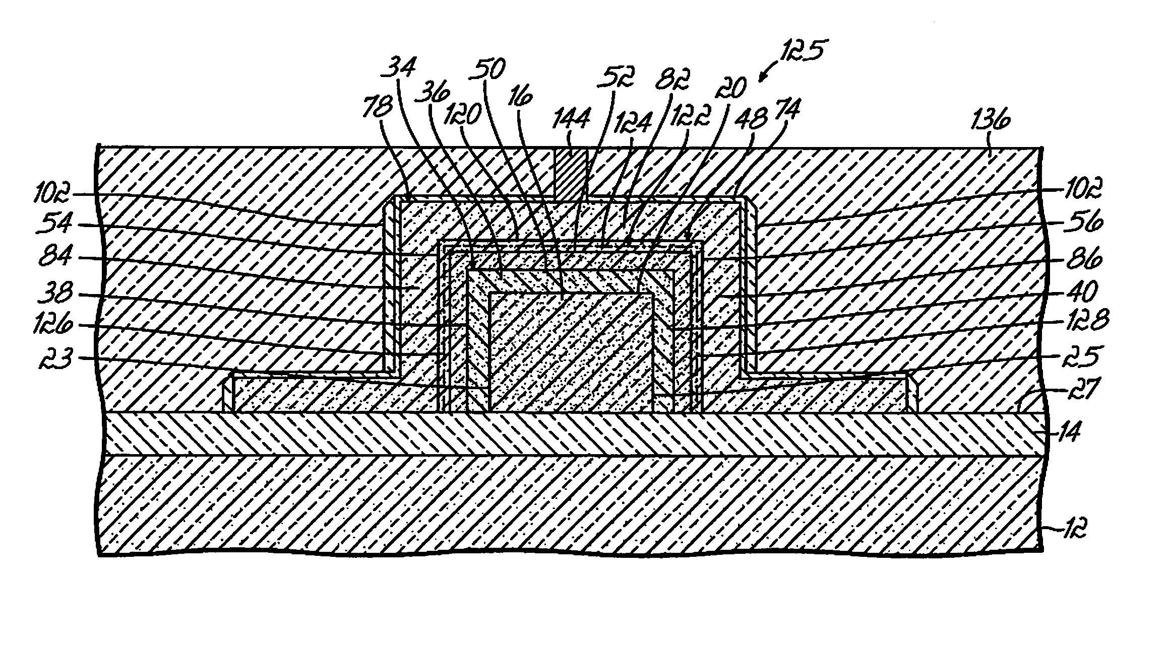
Lateral bicmos replacement metal gate
PatentActiveUS20170005085A1
Innovation
- A method is introduced that involves depositing a high-k dielectric layer and a dummy titanium nitride layer in recesses formed after removing dummy gates, followed by the deposition of a silicon cap layer and selective ion implantation in BJT regions, allowing for the formation of metal gates and optimizing the integration of CMOS and BJT devices in a shared semiconductor substrate.


Hybrid Field Effect Transistor and Bipolar Junction Transistor Structures and Methods for Fabricating Such Structures
PatentInactiveUS20080001234A1
Innovation
- The integration of non-planar bipolar junction transistors and field effect transistors on a common silicon-on-insulator (SOI) substrate, where semiconductor bodies with fin structures are used, allowing for the formation of electrically-isolated regions with different conductivity types to define junctions, enabling a three-dimensional, non-planar device structure.

Manufacturing Process Compatibility Standards
Manufacturing process compatibility represents a critical consideration when integrating MOSFET and BiCMOS technologies into complex network architectures. The fundamental challenge lies in reconciling the distinct fabrication requirements of these technologies while maintaining adherence to industry-standard manufacturing protocols. MOSFET devices typically require simpler process flows with fewer mask layers, whereas BiCMOS integration demands more sophisticated fabrication sequences that accommodate both bipolar and CMOS elements on the same substrate.
Process temperature compatibility emerges as a primary constraint in mixed-technology integration. MOSFET fabrication generally operates within standard CMOS thermal budgets, typically not exceeding 1000°C during critical processing steps. BiCMOS manufacturing, however, requires additional high-temperature processes for bipolar device formation, including emitter and collector implantation steps that can stress existing MOSFET structures. This thermal incompatibility necessitates careful process sequencing and often requires protective measures to preserve device integrity.
Contamination control standards present another significant compatibility challenge. BiCMOS processes introduce additional metallic species and dopants that can compromise MOSFET performance if not properly managed. Cross-contamination between process tools used for different technology nodes requires stringent cleaning protocols and dedicated equipment sets, substantially increasing manufacturing complexity and cost.
Lithography alignment and overlay specifications must accommodate the precision requirements of both technologies simultaneously. While MOSFET devices in advanced nodes demand sub-nanometer overlay accuracy, BiCMOS integration adds complexity through additional mask layers and varying critical dimension requirements across different device types within the same die.
Yield optimization becomes increasingly challenging when combining these technologies, as defect mechanisms from each process flow can compound. Statistical process control must account for the interaction effects between MOSFET and BiCMOS manufacturing steps, requiring enhanced monitoring capabilities and more sophisticated yield modeling approaches.
Quality assurance protocols must encompass the expanded parameter space introduced by mixed-technology integration, including electrical characterization of both digital and analog performance metrics across varying process corners and environmental conditions.
Power Efficiency Optimization in Complex Networks
Power efficiency optimization represents a critical design consideration when integrating MOSFET and BiCMOS technologies into complex network architectures. The fundamental differences in power consumption characteristics between these technologies directly impact overall system performance, thermal management, and operational costs in large-scale network deployments.
MOSFET-based solutions demonstrate superior power efficiency in digital switching applications due to their inherently low static power consumption and fast switching characteristics. The absence of bipolar junction elements eliminates base current requirements, resulting in minimal leakage currents during standby operations. This advantage becomes particularly pronounced in network processors handling intermittent traffic loads, where devices frequently transition between active and idle states.
BiCMOS technology presents a more complex power profile, combining the low static power of CMOS with the high-speed capabilities of bipolar transistors. While BiCMOS circuits typically consume more power during operation compared to pure CMOS implementations, they offer significant advantages in high-frequency analog and mixed-signal applications common in network infrastructure. The bipolar components enable superior drive strength and reduced propagation delays, potentially offsetting increased power consumption through enhanced processing efficiency.
Dynamic power optimization strategies differ substantially between the two technologies. MOSFET implementations benefit from voltage scaling techniques, where supply voltages can be reduced during low-performance periods to achieve quadratic power savings. Advanced power management schemes, including dynamic voltage and frequency scaling, prove highly effective in MOSFET-based network processors.
BiCMOS systems require more sophisticated power optimization approaches due to the dual nature of their transistor types. Selective activation of bipolar stages only when high-speed operation is required, combined with aggressive power gating of unused circuit blocks, enables significant power reductions. Additionally, careful circuit partitioning between CMOS and bipolar sections optimizes the power-performance trade-off across different network functions.
Thermal considerations play a crucial role in power efficiency optimization for complex networks. MOSFET technologies generally exhibit better thermal characteristics due to lower power densities, enabling more aggressive integration and reduced cooling requirements. BiCMOS implementations may require enhanced thermal management solutions but can achieve higher performance per unit area, potentially reducing overall system power through improved integration density.
Unlock deeper insights with Patsnap Eureka Quick Research — get a full tech report to explore trends and direct your research. Try now!
Generate Your Research Report Instantly with AI Agent
Supercharge your innovation with Patsnap Eureka AI Agent Platform!