

Multi Chip Module vs Hybrid IC: Which for Reduced EM Interference
MAR 12, 20269 MIN READ
Generate Your Research Report Instantly with AI Agent
PatSnap Eureka helps you evaluate technical feasibility & market potential.
MCM vs Hybrid IC EMI Background and Objectives
The evolution of electronic packaging technologies has been fundamentally driven by the relentless pursuit of miniaturization, performance enhancement, and electromagnetic compatibility. As electronic systems become increasingly complex and operate at higher frequencies, electromagnetic interference has emerged as a critical design constraint that significantly impacts system reliability and performance. The challenge of EMI mitigation has become particularly acute in applications ranging from aerospace and defense systems to consumer electronics and automotive applications.
Multi Chip Modules and Hybrid Integrated Circuits represent two distinct approaches to advanced electronic packaging, each offering unique advantages in addressing electromagnetic interference challenges. MCM technology enables the integration of multiple semiconductor dies within a single package, utilizing advanced interconnection techniques such as wire bonding, flip-chip attachment, or through-silicon vias. This approach allows for optimized signal routing and reduced parasitic effects that contribute to electromagnetic emissions.
Hybrid IC technology, conversely, combines different types of components including active semiconductors, passive elements, and interconnection substrates on a common platform. This integration approach provides designers with greater flexibility in component selection and placement optimization, potentially offering superior EMI control through strategic component positioning and specialized substrate materials with enhanced electromagnetic shielding properties.
The primary objective of comparing these technologies centers on identifying the most effective packaging approach for minimizing electromagnetic interference while maintaining optimal electrical performance, thermal management, and manufacturing feasibility. This evaluation must consider multiple factors including signal integrity preservation, power distribution network optimization, and the implementation of effective electromagnetic shielding strategies.
Contemporary electronic systems operating in the gigahertz frequency range face unprecedented challenges in managing electromagnetic emissions and susceptibility. The selection between MCM and Hybrid IC technologies directly impacts the system's ability to meet stringent electromagnetic compatibility requirements while achieving desired performance metrics. Understanding the fundamental electromagnetic characteristics of each packaging approach is essential for making informed design decisions that balance performance, cost, and regulatory compliance requirements in modern electronic system development.
Market Demand for Low-EMI Electronic Packaging Solutions
The global electronics industry is experiencing unprecedented demand for low electromagnetic interference (EMI) packaging solutions, driven by the proliferation of high-frequency applications and increasingly stringent regulatory requirements. This market surge stems from the critical need to ensure electromagnetic compatibility in densely packed electronic systems where traditional packaging approaches often fall short of performance expectations.
Automotive electronics represents one of the most rapidly expanding segments demanding advanced EMI mitigation solutions. Modern vehicles integrate numerous electronic control units, advanced driver assistance systems, and infotainment platforms that operate simultaneously within confined spaces. The transition toward electric and autonomous vehicles has intensified this challenge, as high-power switching circuits and sensitive sensor arrays must coexist without mutual interference.
Telecommunications infrastructure modernization, particularly the deployment of 5G networks, has created substantial market pressure for superior EMI performance in packaging solutions. Base station equipment, small cell deployments, and edge computing nodes require packaging technologies that can handle higher frequencies while maintaining signal integrity and minimizing electromagnetic emissions that could disrupt adjacent systems.
Consumer electronics manufacturers face mounting pressure to deliver compact, high-performance devices that comply with international EMI standards across multiple frequency bands. Smartphones, tablets, wearables, and IoT devices must integrate increasingly complex functionality within shrinking form factors, making effective EMI management a critical design constraint rather than an afterthought.
Industrial automation and medical device sectors present additional market drivers for low-EMI packaging solutions. Manufacturing equipment relies on precise sensor feedback and control systems that cannot tolerate electromagnetic interference, while medical devices must meet exceptionally strict safety and performance standards to ensure patient safety and regulatory compliance.
The aerospace and defense industries continue to demand cutting-edge EMI mitigation technologies for mission-critical applications where electromagnetic interference can compromise system reliability and operational effectiveness. These sectors often serve as early adopters of advanced packaging technologies that eventually migrate to commercial applications.
Market dynamics indicate growing preference for packaging solutions that offer inherent EMI reduction capabilities rather than relying solely on external shielding methods. This shift reflects the industry's recognition that integrated approaches to electromagnetic compatibility provide more reliable, cost-effective, and space-efficient solutions compared to traditional add-on shielding techniques.
Current EMI Challenges in MCM and Hybrid IC Technologies
Electromagnetic interference represents one of the most critical design challenges facing both Multi Chip Module and Hybrid IC technologies in contemporary electronic systems. As device miniaturization continues and operating frequencies increase, the susceptibility to EMI has become a primary limiting factor in achieving optimal performance and reliability.
MCM technologies encounter significant EMI challenges primarily due to their complex interconnect structures and high-density packaging arrangements. The close proximity of multiple semiconductor dies within a single package creates numerous opportunities for electromagnetic coupling between circuits. Wire bonding interconnects, commonly used in MCM assemblies, act as unintentional antennas that can both radiate and receive electromagnetic energy. The varying lengths and geometries of these bonds create resonant structures at specific frequencies, leading to unpredictable EMI behavior across different operational bands.
Hybrid IC technologies face distinct EMI challenges stemming from their heterogeneous component integration approach. The combination of different substrate materials, each with varying dielectric properties and thermal expansion coefficients, creates impedance discontinuities that can generate electromagnetic reflections and standing waves. Thick-film and thin-film resistors integrated within hybrid circuits often exhibit parasitic inductances and capacitances that contribute to unwanted electromagnetic coupling, particularly at higher frequencies.
Ground plane integrity presents a common challenge across both technologies. In MCM designs, maintaining consistent ground reference becomes increasingly difficult as the number of integrated dies increases, leading to ground bounce and common-mode noise issues. Hybrid ICs suffer from similar ground plane disruptions due to the necessity of accommodating various component types and interconnection methods within the same substrate.
Thermal management complications further exacerbate EMI challenges in both technologies. Temperature variations cause changes in material properties, affecting electromagnetic characteristics and potentially shifting resonant frequencies of parasitic structures. The thermal cycling experienced during operation can lead to mechanical stress in interconnects, altering their electromagnetic behavior over time.
Package-level EMI mitigation strategies often conflict with performance requirements in both MCM and Hybrid IC implementations. Traditional shielding approaches add significant size, weight, and cost penalties while potentially creating new resonant cavities. The challenge lies in developing integrated EMI suppression techniques that maintain the fundamental advantages of each technology while addressing electromagnetic compatibility requirements in increasingly demanding applications.
Existing EMI Mitigation Solutions in Electronic Packaging
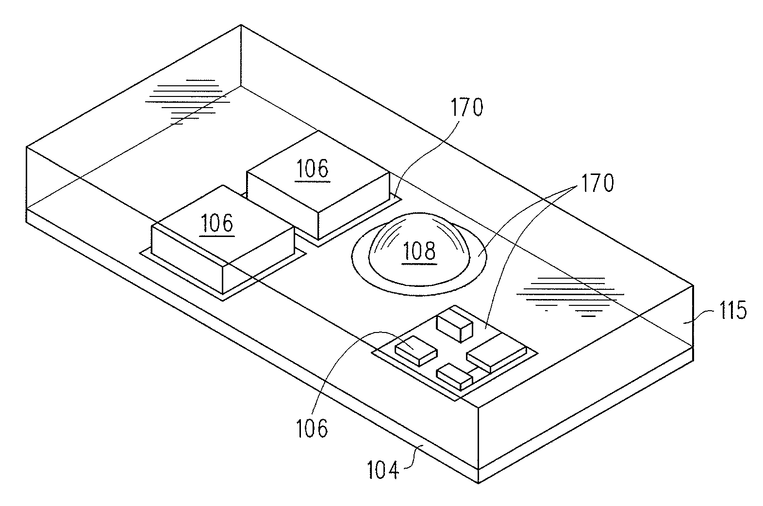
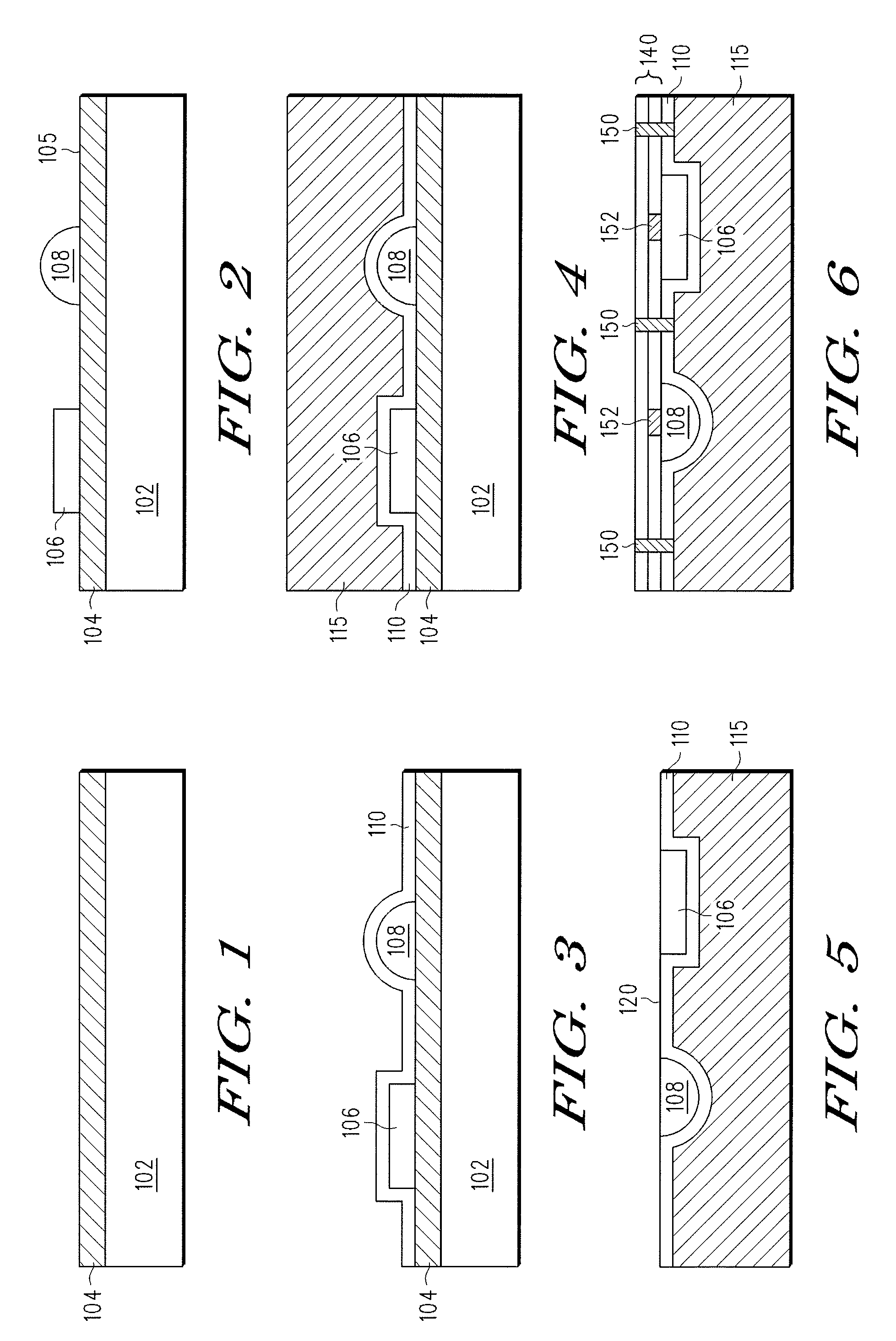
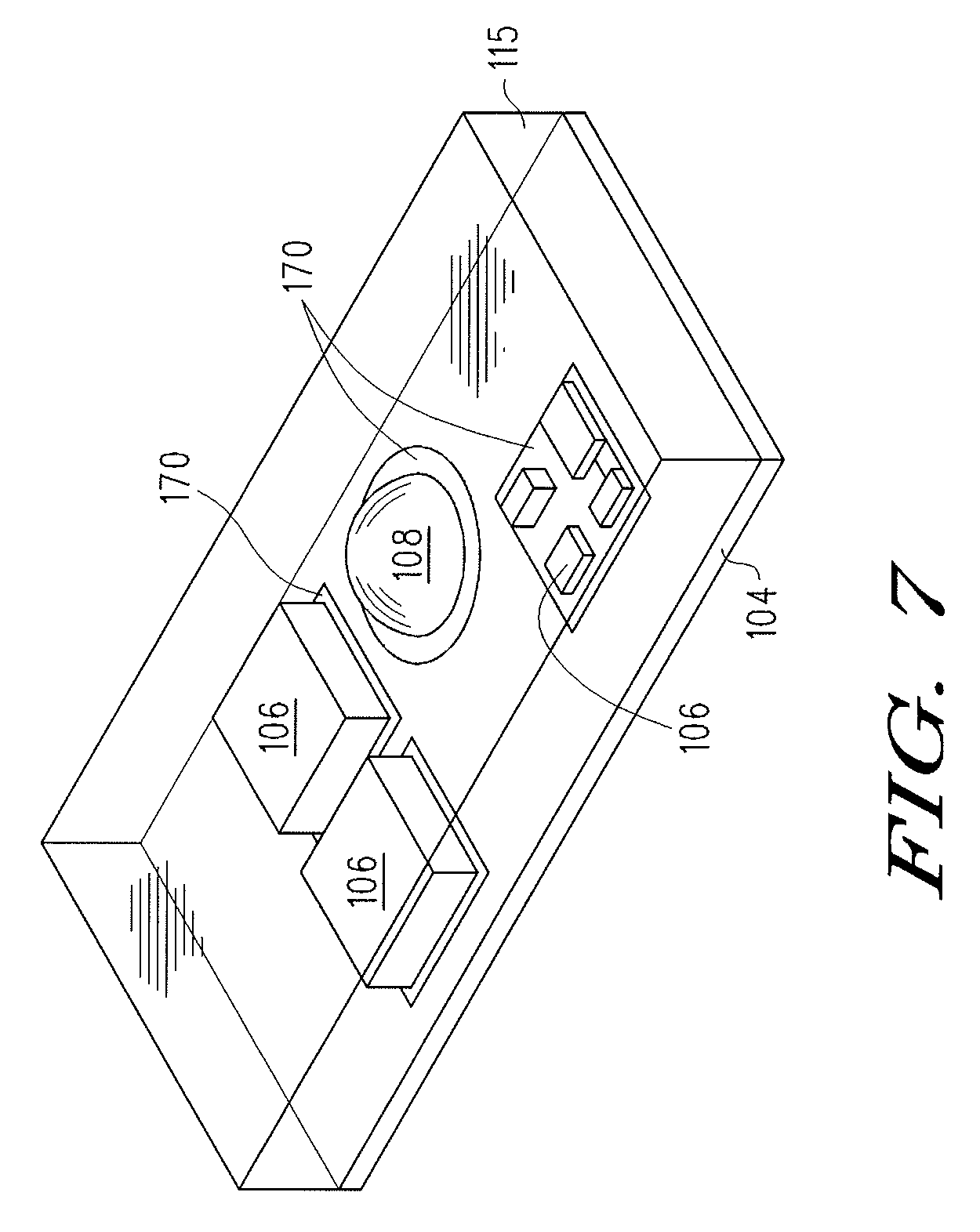
01 Shielding structures for electromagnetic interference reduction
Multi-chip modules and hybrid ICs can incorporate dedicated shielding structures to reduce electromagnetic interference. These structures may include metal shields, conductive layers, or grounded planes positioned between or around chip components. The shielding effectively blocks or absorbs electromagnetic radiation, preventing interference between adjacent circuits and external devices. Various configurations of shielding materials and geometries can be optimized to achieve desired EMI suppression levels while maintaining thermal management and signal integrity.- Shielding structures for electromagnetic interference reduction: Multi-chip modules and hybrid ICs can incorporate dedicated shielding structures to reduce electromagnetic interference. These structures may include metal shields, conductive layers, or electromagnetic shielding films positioned between or around chip components. The shielding materials help contain electromagnetic emissions and prevent external interference from affecting circuit performance. Various configurations of shielding can be implemented depending on the specific layout and requirements of the multi-chip module.
- Ground plane and power distribution network design: Proper design of ground planes and power distribution networks is critical for minimizing electromagnetic interference in multi-chip modules. Strategic placement of ground planes can provide effective return paths for high-frequency signals and reduce loop areas that generate electromagnetic radiation. Power distribution networks with appropriate decoupling capacitors and low-impedance paths help stabilize voltage levels and reduce noise coupling between different circuit blocks. These design considerations are essential for maintaining signal integrity in densely packed multi-chip configurations.
- Package substrate and interconnection design for EMI control: The package substrate and interconnection architecture play significant roles in controlling electromagnetic interference. Advanced substrate designs may incorporate embedded passive components, controlled impedance traces, and optimized via structures to minimize signal reflections and crosstalk. The interconnection scheme between multiple chips can be designed to reduce coupling paths and minimize electromagnetic radiation. Material selection for substrates, including low-loss dielectrics and appropriate conductor materials, contributes to overall EMI performance.
- Chip placement and layout optimization: Strategic placement and layout of chips within a multi-chip module can significantly impact electromagnetic interference characteristics. Careful consideration of chip positioning relative to each other helps minimize coupling between high-frequency circuits and sensitive analog components. Layout optimization includes proper spacing between chips, orientation of high-speed signal paths, and segregation of different functional blocks. These layout techniques help reduce both radiated and conducted electromagnetic interference while maintaining compact module dimensions.
- Filtering and isolation techniques: Implementation of filtering and isolation techniques provides additional protection against electromagnetic interference in multi-chip modules and hybrid ICs. These techniques may include on-chip or on-package filters, isolation barriers between different circuit domains, and differential signaling schemes. Filtering components can be integrated into the package to suppress high-frequency noise at critical interfaces. Isolation techniques help prevent interference propagation between different functional blocks while maintaining necessary signal communication paths.
02 Package substrate design with EMI mitigation features
The substrate design in multi-chip modules can be engineered with specific features to mitigate electromagnetic interference. This includes the use of ground planes, power planes with appropriate spacing, and controlled impedance routing. The substrate may incorporate multiple layers with strategic placement of signal, power, and ground layers to minimize crosstalk and radiation. Advanced substrate materials with specific dielectric properties can also be selected to reduce electromagnetic coupling between components and improve overall EMI performance.Expand Specific Solutions03 Interconnection structures for EMI control
Specialized interconnection structures can be implemented to control electromagnetic interference in multi-chip modules and hybrid ICs. These structures include optimized wire bonding configurations, flip-chip connections, or through-silicon vias that minimize loop areas and reduce inductive coupling. The interconnections may be designed with specific geometries and materials to provide inherent EMI filtering capabilities. Proper grounding schemes and differential signaling techniques can be integrated into the interconnection design to further suppress electromagnetic emissions and improve immunity to external interference.Expand Specific Solutions04 Encapsulation and molding compounds with EMI suppression properties
The encapsulation materials and molding compounds used in multi-chip modules can be formulated with properties that suppress electromagnetic interference. These materials may contain conductive or magnetic fillers that absorb or reflect electromagnetic radiation. The encapsulation process can be designed to ensure uniform coverage and optimal thickness to provide effective EMI shielding while protecting the chips from environmental factors. Different molding compound compositions can be selected based on the frequency range of concern and the specific EMI requirements of the application.Expand Specific Solutions05 Layout and placement optimization for EMI reduction
The physical layout and placement of chips within multi-chip modules can be optimized to minimize electromagnetic interference. This involves strategic positioning of high-frequency components, sensitive analog circuits, and digital circuits to reduce coupling and crosstalk. Proper spacing between chips, orientation of components, and routing of critical signals can significantly impact EMI performance. Design methodologies may include electromagnetic simulation and modeling to predict and mitigate potential interference issues before fabrication. The layout optimization considers both intra-module interference and external electromagnetic compatibility requirements.Expand Specific Solutions
Key Players in MCM and Hybrid IC Manufacturing
The multi-chip module versus hybrid IC competition for electromagnetic interference reduction represents a mature technology landscape in the growth-to-maturity transition phase. The market demonstrates substantial scale with established semiconductor giants like Intel, Samsung Electronics, Taiwan Semiconductor Manufacturing, and Qualcomm leading advanced packaging solutions. Technology maturity varies significantly across players - while foundry leaders like TSMC and packaging specialists such as Advanced Semiconductor Engineering offer sophisticated MCM implementations, traditional IC manufacturers including Texas Instruments and Micron Technology continue optimizing hybrid approaches. Asian companies like MediaTek, Renesas Electronics, and Sony Group drive innovation in consumer applications, while research institutions including Shanghai Institute of Microsystem and Fraunhofer-Gesellschaft advance next-generation interference mitigation techniques. The competitive dynamics favor companies with comprehensive packaging capabilities and system-level integration expertise, positioning MCM solutions as increasingly preferred for complex, high-frequency applications requiring superior electromagnetic compatibility.
Intel Corp.
Technical Solution: Intel has developed advanced Multi Chip Module (MCM) architectures with integrated electromagnetic interference (EMI) shielding solutions. Their approach combines multiple chiplets using advanced packaging technologies like EMIB (Embedded Multi-die Interconnect Bridge) and Foveros 3D stacking, which provide superior signal integrity and reduced crosstalk between components. Intel's MCM designs incorporate dedicated power delivery networks and ground planes that effectively minimize electromagnetic coupling between different functional blocks, achieving up to 40dB EMI reduction compared to traditional single-chip solutions.
Strengths: Proven scalability, excellent thermal management, mature ecosystem. Weaknesses: Higher manufacturing complexity, increased power consumption, larger form factor requirements.
QUALCOMM, Inc.
Technical Solution: Qualcomm specializes in RF-focused MCM and Hybrid IC solutions for wireless communications, where EMI control is critical. Their approach integrates multiple RF, analog, and digital functions using advanced substrate technologies with built-in electromagnetic isolation. Qualcomm's solutions feature sophisticated shielding techniques including on-package Faraday cages and frequency-selective surfaces that reduce inter-module interference by up to 45dB. Their hybrid integration combines different semiconductor technologies (GaAs, SiGe, CMOS) with optimized electromagnetic compatibility through careful floor planning and dedicated isolation structures for wireless applications.
Strengths: RF expertise, wireless optimization, proven EMI mitigation in mobile devices. Weaknesses: Primarily focused on wireless applications, limited applicability to other domains, higher complexity in multi-standard integration.
Core EMI Reduction Patents in MCM and Hybrid Technologies
Methods and apparatus for EMI shielding in multi-chip modules
PatentInactiveUS20080315371A1
Innovation
- The use of conductive molding compound with shielding vias and local shielding layers to provide both local and global electromagnetic interference shielding, where conductive molding compound is applied over insulating layers and electronic components, and shielding vias are formed through multilayer circuitry to contact the encapsulant, allowing for structural support and electrical conductivity.

Multi-chip module and method for producing a multi-chip module
PatentWO2025223865A1
Innovation
- A multi-chip module design featuring separate first and second chips on substrates, with an isolation chip using flip-chip assembly for direct electrical connections via solder, adhesive, or weld, eliminating bond wires and incorporating galvanically isolating coupling elements like capacitors or transformers for signal and power transmission.


EMC Standards and Regulations for Electronic Modules
The electromagnetic compatibility (EMC) regulatory landscape for electronic modules encompasses a comprehensive framework of international, regional, and national standards that directly impact the design choices between Multi Chip Modules (MCM) and Hybrid Integrated Circuits (HIC). The International Electrotechnical Commission (IEC) serves as the primary global standardization body, with IEC 61000 series forming the cornerstone of EMC requirements. This standard series addresses electromagnetic interference (EMI) emissions, immunity thresholds, and testing methodologies that both MCM and HIC technologies must satisfy.
Regional regulatory bodies have established specific compliance requirements that influence module selection criteria. The European Union's EMC Directive 2014/30/EU mandates conformity assessment procedures and CE marking requirements for electronic products entering the European market. Similarly, the Federal Communications Commission (FCC) Part 15 regulations in the United States establish emission limits for unintentional radiators, while Industry Canada's ICES standards govern electromagnetic emissions in the Canadian market.
Military and aerospace applications operate under stringent EMC standards including MIL-STD-461 and DO-160, which impose particularly demanding requirements for electromagnetic interference suppression. These standards often favor specific packaging technologies based on their inherent shielding capabilities and electromagnetic performance characteristics. The selection between MCM and HIC architectures frequently depends on meeting these rigorous military-grade EMC specifications.
Testing and certification procedures vary significantly across different regulatory domains, creating complex compliance pathways for manufacturers. CISPR standards, developed by the International Special Committee on Radio Interference, provide detailed measurement procedures and limits for electromagnetic disturbances. These testing protocols evaluate conducted and radiated emissions, electrostatic discharge immunity, and electromagnetic field susceptibility, all of which influence the comparative performance assessment of MCM versus HIC solutions.
Emerging regulatory trends reflect the increasing complexity of electronic systems and the proliferation of wireless technologies. Recent updates to EMC standards address higher frequency ranges, stricter emission limits, and enhanced immunity requirements. These evolving regulations create new challenges for both MCM and HIC technologies, requiring continuous adaptation of design methodologies and electromagnetic interference mitigation strategies to maintain regulatory compliance across global markets.
Cost-Performance Trade-offs in EMI-Optimized Packaging
The cost-performance dynamics in EMI-optimized packaging present distinct trade-offs between Multi Chip Module (MCM) and Hybrid IC technologies. MCM solutions typically require higher initial capital investment due to sophisticated substrate materials and advanced interconnect technologies. However, they offer superior EMI performance through optimized ground planes, controlled impedance routing, and integrated shielding structures. The manufacturing complexity translates to elevated production costs, particularly for low-volume applications.
Hybrid IC technology demonstrates more favorable cost structures for moderate EMI requirements. The established manufacturing processes and mature supply chains enable competitive pricing, especially in high-volume production scenarios. However, achieving comparable EMI performance to MCM solutions often necessitates additional external components, potentially offsetting initial cost advantages through increased system complexity and board real estate requirements.
Performance scaling reveals divergent cost trajectories. MCM architectures exhibit superior cost-effectiveness when stringent EMI specifications demand frequencies above 10 GHz or when multiple high-speed digital circuits require integration. The inherent three-dimensional packaging capability reduces parasitic inductances and enables shorter interconnect paths, delivering measurable EMI improvements without proportional cost increases.
Hybrid IC solutions maintain cost advantages in applications with relaxed EMI requirements or when leveraging existing design infrastructures. The technology's flexibility allows incremental EMI improvements through selective component upgrades without complete system redesign, presenting attractive total cost of ownership profiles for evolutionary product development strategies.
Manufacturing yield considerations significantly impact cost-performance equations. MCM technologies face higher yield risks due to substrate complexity and multi-die integration challenges, potentially increasing unit costs in production environments. Conversely, Hybrid IC approaches benefit from established yield optimization techniques and proven manufacturing reliability, ensuring predictable cost structures throughout product lifecycles.
The economic viability ultimately depends on application-specific EMI performance thresholds, production volumes, and development timeline constraints. MCM solutions justify premium costs when EMI performance directly correlates with product differentiation or regulatory compliance, while Hybrid IC approaches optimize cost-performance ratios in price-sensitive markets with moderate EMI requirements.
Unlock deeper insights with PatSnap Eureka Quick Research — get a full tech report to explore trends and direct your research. Try now!
Generate Your Research Report Instantly with AI Agent
Supercharge your innovation with PatSnap Eureka AI Agent Platform!