

Optimize Ceramic Substrates For Better Dielectric Stability
MAY 26, 20269 MIN READ
Generate Your Research Report Instantly with AI Agent
PatSnap Eureka helps you evaluate technical feasibility & market potential.
Ceramic Substrate Dielectric Evolution and Targets
Ceramic substrates have undergone significant evolution since their introduction in the mid-20th century, transitioning from basic alumina-based materials to sophisticated engineered compositions. The initial development focused primarily on mechanical strength and thermal conductivity, with dielectric properties being secondary considerations. Early ceramic substrates exhibited substantial dielectric variations under temperature and frequency changes, limiting their application in precision electronic systems.
The evolution accelerated during the 1980s and 1990s as electronic miniaturization demands intensified. Advanced ceramic compositions incorporating titanium dioxide, barium titanate, and various rare earth oxides emerged to address dielectric stability challenges. These developments marked a paradigm shift toward engineered dielectric properties rather than accepting inherent material limitations.
Modern ceramic substrate development emphasizes multi-phase compositions and controlled microstructures to achieve stable dielectric performance. The integration of low-loss ceramic phases with temperature-compensating additives has become standard practice. Contemporary substrates demonstrate dielectric constant variations below 1% across operational temperature ranges, representing a hundredfold improvement over early materials.
Current technological targets focus on achieving ultra-stable dielectric performance across extended frequency ranges from DC to millimeter-wave applications. The primary objective involves maintaining dielectric constant stability within ±0.5% over temperature ranges spanning -55°C to +125°C. Additionally, loss tangent values below 0.001 at microwave frequencies represent critical performance benchmarks for next-generation applications.
Future development targets encompass adaptive dielectric properties through smart material integration and real-time compensation mechanisms. The ultimate goal involves creating ceramic substrates with programmable dielectric characteristics that can dynamically adjust to optimize circuit performance under varying operational conditions, potentially revolutionizing high-frequency electronic system design and reliability standards.
Market Demand for High-Performance Ceramic Substrates
The global electronics industry's relentless pursuit of miniaturization and enhanced performance has created substantial demand for high-performance ceramic substrates with superior dielectric stability. This demand stems primarily from the telecommunications sector, where 5G infrastructure deployment requires components capable of operating at higher frequencies while maintaining signal integrity. The automotive electronics market represents another significant growth driver, particularly with the proliferation of electric vehicles and advanced driver assistance systems that demand reliable ceramic substrates for power electronics and sensor applications.
Consumer electronics manufacturers increasingly require ceramic substrates that can withstand thermal cycling and maintain consistent dielectric properties across varying environmental conditions. The Internet of Things expansion has further amplified this need, as billions of connected devices require compact, reliable substrates that can perform consistently over extended operational periods. Medical device manufacturers also contribute to market demand, seeking ceramic substrates with exceptional stability for implantable devices and diagnostic equipment where reliability is paramount.
The aerospace and defense sectors represent high-value market segments demanding ceramic substrates with stringent performance specifications. These applications require materials that maintain dielectric stability under extreme temperature variations, radiation exposure, and mechanical stress. The growing satellite communication market, including low Earth orbit constellation deployments, has intensified requirements for ceramic substrates that can operate reliably in harsh space environments.
Market dynamics reveal increasing customer willingness to invest in premium ceramic substrate solutions that offer enhanced dielectric stability, even at higher costs, due to the total cost of ownership benefits. System-level reliability improvements achieved through superior ceramic substrates often justify premium pricing, particularly in mission-critical applications where failure costs are substantial.
Regional market analysis indicates strong demand concentration in Asia-Pacific manufacturing hubs, North American technology centers, and European automotive electronics clusters. The market exhibits growing sophistication, with customers increasingly specifying detailed dielectric stability requirements rather than accepting standard offerings. This trend toward customization and performance optimization creates opportunities for ceramic substrate manufacturers who can deliver tailored solutions meeting specific application requirements while maintaining cost competitiveness in high-volume production scenarios.
Current Dielectric Stability Challenges in Ceramics
Ceramic substrates face significant dielectric stability challenges that directly impact their performance in electronic applications. Temperature-induced variations represent one of the most critical issues, as ceramic materials exhibit substantial changes in dielectric constant and loss tangent across operating temperature ranges. These fluctuations can cause frequency drift in resonators, impedance mismatches in transmission lines, and degraded signal integrity in high-frequency circuits.
Frequency-dependent dielectric behavior poses another major challenge for ceramic substrates. Many ceramic compositions demonstrate non-linear dielectric responses at different frequencies, particularly in the microwave and millimeter-wave ranges. This frequency dispersion leads to unpredictable electrical performance and complicates circuit design processes, especially for broadband applications requiring consistent dielectric properties across wide frequency spectrums.
Moisture absorption significantly affects dielectric stability in ceramic substrates. Even low-porosity ceramics can absorb atmospheric moisture, which alters their dielectric constant and increases dielectric losses. This hygroscopic behavior creates time-dependent variations in electrical properties, making long-term performance prediction difficult and potentially compromising device reliability in humid environments.
Manufacturing-induced variations contribute substantially to dielectric instability challenges. Processing parameters such as sintering temperature, cooling rates, and grain size distribution directly influence the final dielectric properties. Batch-to-batch variations in raw materials and processing conditions result in inconsistent dielectric characteristics, making it challenging to achieve reproducible performance across production runs.
Compositional heterogeneity within ceramic substrates creates localized dielectric property variations. Secondary phases, grain boundary effects, and dopant distribution irregularities lead to microscopic dielectric constant fluctuations that can affect overall substrate performance. These inhomogeneities become particularly problematic in high-frequency applications where even small variations can significantly impact circuit behavior.
Aging effects represent long-term dielectric stability challenges in ceramic substrates. Structural relaxation, phase transformations, and defect migration over time can gradually alter dielectric properties. These aging mechanisms are often accelerated by thermal cycling, electrical stress, and environmental exposure, leading to drift in circuit performance and reduced device lifespan.
External field dependencies further complicate dielectric stability in ceramic substrates. High electric field strengths can induce non-linear dielectric responses, while mechanical stress from thermal expansion mismatches or external forces can alter dielectric properties through piezoelectric and electrostrictive effects. These field-dependent behaviors create additional sources of instability that must be carefully managed in practical applications.
Existing Dielectric Optimization Solutions
01 Ceramic substrate composition optimization for dielectric stability
Optimization of ceramic substrate compositions through specific material formulations and additive incorporation to enhance dielectric properties and maintain stability under various operating conditions. This involves careful selection of base ceramic materials and dopants to achieve desired dielectric constants and minimize losses.- Ceramic substrate composition optimization for dielectric stability: Optimization of ceramic substrate compositions through specific material formulations and additive incorporation to enhance dielectric properties and maintain stability under various operating conditions. This involves careful selection of base ceramic materials and dopants to achieve desired dielectric constants and minimize losses over temperature and frequency ranges.
- Temperature coefficient control in ceramic dielectrics: Methods for controlling temperature coefficients of dielectric properties in ceramic substrates to ensure stable performance across operating temperature ranges. This includes the use of compensating materials and specific processing techniques to minimize temperature-dependent variations in dielectric constant and loss tangent.
- Processing techniques for enhanced dielectric stability: Manufacturing and processing methods including sintering conditions, atmosphere control, and thermal treatment cycles that improve the dielectric stability of ceramic substrates. These techniques focus on achieving uniform microstructure and minimizing defects that could affect dielectric performance over time.
- Multilayer ceramic substrate dielectric design: Design approaches for multilayer ceramic substrates that maintain dielectric stability through layer composition control, interface optimization, and co-firing compatibility. This includes considerations for layer thickness uniformity and interlayer adhesion to prevent delamination and maintain consistent dielectric properties.
- Dielectric loss minimization and aging resistance: Strategies for minimizing dielectric losses and improving aging resistance in ceramic substrates through microstructural control, grain boundary engineering, and the incorporation of stabilizing agents. These approaches focus on maintaining long-term stability of dielectric properties under operational stress and environmental conditions.
02 Temperature coefficient control in ceramic dielectrics
Methods for controlling temperature coefficients of ceramic substrates to ensure dielectric stability across wide temperature ranges. This includes formulation strategies and processing techniques that minimize temperature-dependent variations in dielectric properties, ensuring consistent performance in electronic applications.Expand Specific Solutions03 Processing and sintering techniques for enhanced stability
Advanced processing and sintering methods to improve the microstructure and dielectric stability of ceramic substrates. These techniques focus on controlling grain size, porosity, and phase formation during manufacturing to achieve optimal dielectric performance and long-term stability.Expand Specific Solutions04 Multilayer ceramic substrate design for dielectric performance
Design and fabrication approaches for multilayer ceramic substrates that maintain dielectric stability while providing enhanced functionality. This includes layer interface optimization, material compatibility considerations, and structural designs that prevent delamination and maintain consistent dielectric properties.Expand Specific Solutions05 Testing and characterization methods for dielectric stability assessment
Comprehensive testing methodologies and characterization techniques for evaluating the dielectric stability of ceramic substrates under various environmental and operational conditions. These methods enable accurate assessment of long-term performance and reliability in electronic applications.Expand Specific Solutions
Leading Ceramic Substrate Manufacturers Analysis
The ceramic substrate optimization market for enhanced dielectric stability represents a mature yet rapidly evolving sector driven by increasing demands from 5G communications, automotive electronics, and power electronics applications. The industry has reached significant scale with established players like Murata Manufacturing, TDK Corp., and Kyocera Corp. dominating through decades of ceramic expertise and manufacturing capabilities. Technology maturity varies across segments, with companies like Samsung Electro-Mechanics and Taiyo Yuden advancing multilayer ceramic capacitor technologies, while emerging players such as Aurora Technologies and Chaozhou Three-Circle focus on specialized thin-film and high-frequency applications. The competitive landscape shows consolidation among Japanese manufacturers maintaining technological leadership, while Chinese companies like China Building Materials Academy are rapidly developing capabilities. Research institutions including Industrial Technology Research Institute and various universities are pushing next-generation materials development, indicating continued innovation potential in substrate composition and processing techniques for superior dielectric performance.
Murata Manufacturing Co. Ltd.
Technical Solution: Murata employs advanced ceramic substrate optimization through proprietary low-temperature co-fired ceramics (LTCC) technology, utilizing high-purity alumina and glass-ceramic composites with precisely controlled grain structures. Their approach involves multi-layer ceramic substrates with embedded passive components, achieving dielectric constants ranging from 4.5 to 90 with temperature coefficients as low as ±15ppm/°C. The company implements advanced sintering processes at temperatures below 900°C, enabling integration of high-conductivity silver electrodes while maintaining excellent dielectric stability across temperature ranges from -55°C to +125°C.
Strengths: Industry-leading miniaturization capabilities and excellent temperature stability. Weaknesses: Higher manufacturing costs and limited customization for specialized applications.
Taiyo Yuden Co., Ltd.
Technical Solution: Taiyo Yuden employs sophisticated ceramic substrate optimization using temperature-stable dielectric formulations based on modified titanate systems with controlled crystal structure modifications. Their approach involves precise control of ceramic powder synthesis through co-precipitation and sol-gel methods, achieving particle sizes below 100nm for improved sintering behavior. The company implements advanced tape casting and screen printing technologies for multilayer substrate fabrication, with layer thickness control within ±2μm. Their substrates achieve dielectric stability with temperature coefficients better than ±30ppm/°C and maintain stable performance under high humidity conditions (85°C/85%RH) for over 1000 hours.
Strengths: Excellent environmental stability and proven reliability in harsh conditions. Weaknesses: Limited high-power applications and relatively narrow frequency range optimization.
Key Patents in Ceramic Dielectric Enhancement
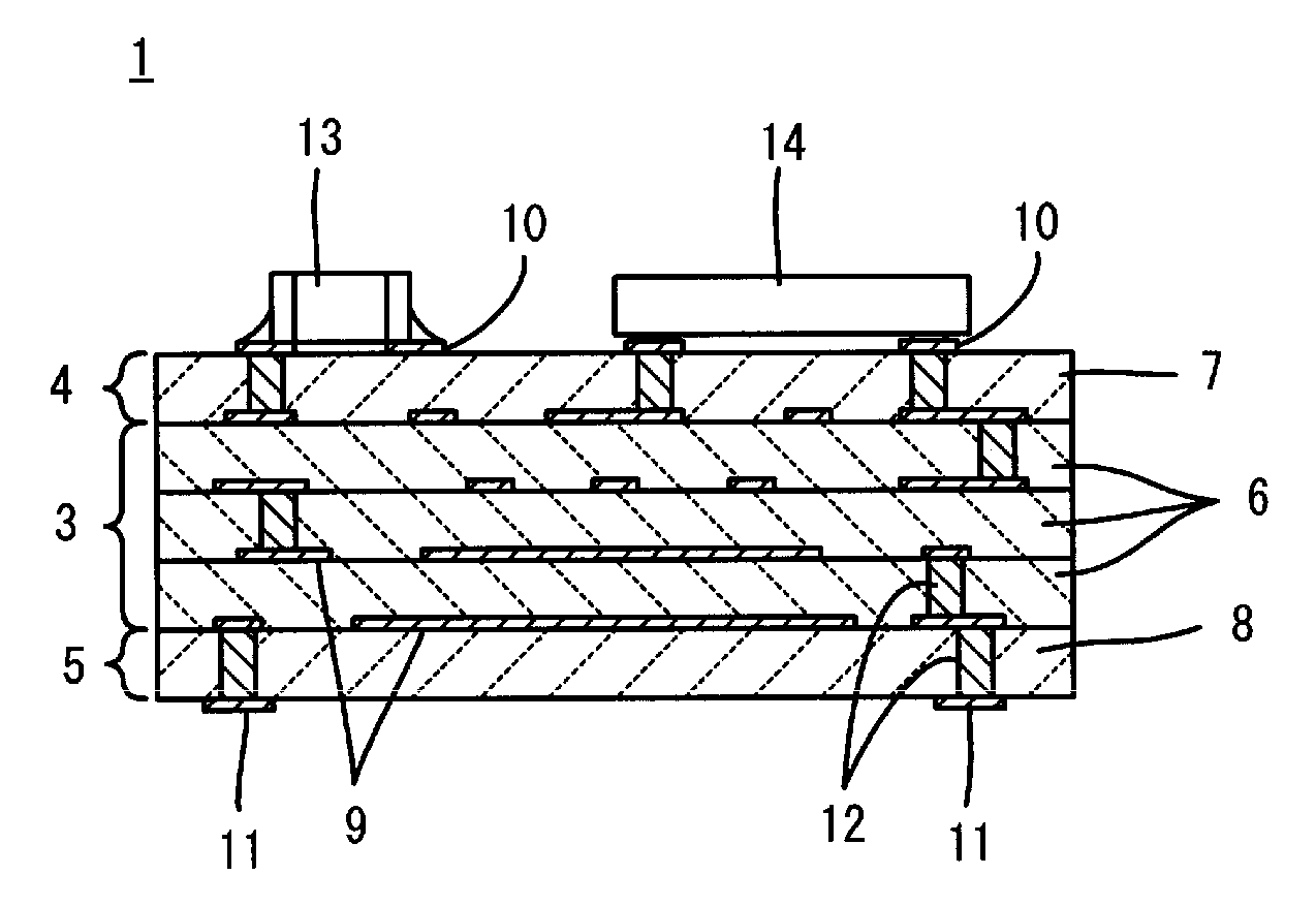
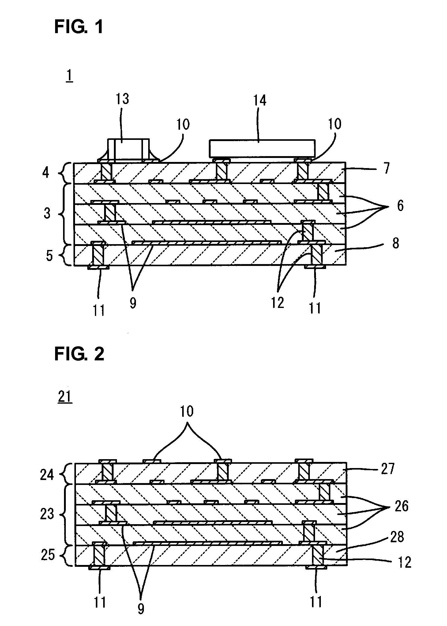
Dielectric ceramic composition, ceramic substrate, and method for producing the same
PatentInactiveUS20090004438A1
Innovation
- A dielectric ceramic composition with specific weight percentages of BaO, SiO2, Al2O3, B2O3, Cr2O3, ZrO2, and optional Y2O3, CaO, MgO, and SrO, forming a laminated structure with tetragonal zirconia, which enhances chemical resistance and flexural strength by controlling thermal expansion coefficients and adhesion.


Ceramic substrate, ceramic circuit substrate, and semiconductor device
PatentPendingEP4592270A1
Innovation
- A ceramic substrate design that ensures a ratio of arc discharge voltage to dielectric breakdown voltage (A/B) of not less than 0.3, with controlled void distribution and specific void characteristics, including a 90 µm × 120 µm region with limited void counts and sizes, to enhance long-term reliability.


Environmental Standards for Ceramic Materials
Environmental standards for ceramic materials have evolved significantly over the past decade, driven by increasing regulatory pressure and sustainability concerns across multiple industries. The ceramic substrate manufacturing sector faces stringent requirements from international bodies including ISO 14001, RoHS directives, and REACH regulations, which directly impact material selection and processing methodologies for dielectric applications.
Current environmental compliance frameworks mandate comprehensive lifecycle assessments for ceramic substrates, encompassing raw material extraction, manufacturing processes, and end-of-life disposal considerations. These standards particularly emphasize the reduction of hazardous substances such as lead-based compounds, which have traditionally been used to enhance dielectric properties in ceramic formulations. The transition away from these materials presents both challenges and opportunities for achieving superior dielectric stability through alternative approaches.
Manufacturing process standards focus heavily on emission control and energy efficiency metrics. Sintering operations, critical for ceramic substrate production, must comply with air quality regulations limiting particulate matter and volatile organic compound emissions. Additionally, water usage and wastewater treatment standards require implementation of closed-loop systems and advanced filtration technologies to minimize environmental impact while maintaining product quality.
Emerging green chemistry principles are reshaping ceramic material development, promoting the use of bio-based precursors and environmentally benign processing aids. These standards encourage the adoption of sol-gel synthesis routes and low-temperature processing techniques that reduce energy consumption while potentially improving dielectric performance through enhanced microstructural control.
Regional variations in environmental standards create additional complexity for global ceramic substrate manufacturers. European WEEE directives impose strict recycling requirements, while Asian markets increasingly adopt carbon footprint limitations. North American standards emphasize workplace safety and chemical exposure limits, influencing material handling protocols and facility design requirements.
Future environmental standards are expected to incorporate circular economy principles, mandating design for recyclability and material recovery. This trend will likely drive innovation toward modular ceramic substrate architectures and reversible bonding technologies, potentially opening new pathways for optimizing dielectric stability through novel material combinations and processing approaches.
Quality Control Methods for Dielectric Properties
Quality control methods for dielectric properties in ceramic substrates require comprehensive testing protocols that ensure consistent performance across production batches. The primary measurement techniques include impedance spectroscopy, which evaluates dielectric constant and loss tangent across frequency ranges from 1 MHz to 40 GHz. This method provides critical insights into material behavior under various operating conditions and enables identification of frequency-dependent variations that could impact circuit performance.
Temperature coefficient testing represents another fundamental quality control approach, measuring dielectric property changes across operational temperature ranges typically spanning -55°C to +125°C. Advanced testing facilities employ environmental chambers with precise temperature control to evaluate thermal stability coefficients, ensuring substrates maintain specified tolerances throughout their service life. Automated measurement systems integrate network analyzers with temperature cycling equipment to generate comprehensive stability profiles.
Moisture absorption testing protocols evaluate how environmental humidity affects dielectric properties over extended periods. Standard procedures involve exposing samples to controlled humidity conditions at 85% relative humidity and 85°C for predetermined durations, followed by dielectric measurements to quantify property degradation. This testing reveals potential long-term reliability issues that could compromise circuit performance in harsh environments.
Statistical process control implementation involves establishing control charts for key dielectric parameters, enabling real-time monitoring of production quality. Manufacturing facilities typically implement sampling strategies that test representative samples from each production lot, with acceptance criteria based on statistical confidence intervals. Advanced facilities employ automated testing systems that can process hundreds of samples daily while maintaining measurement accuracy within ±1% for dielectric constant values.
Non-destructive evaluation techniques include microwave resonator methods and time-domain reflectometry, which allow comprehensive substrate characterization without compromising product integrity. These methods enable 100% inspection capabilities for critical applications while maintaining production throughput requirements. Integration of artificial intelligence algorithms enhances defect detection capabilities by identifying subtle pattern variations that traditional threshold-based systems might miss.
Calibration and traceability protocols ensure measurement accuracy through regular calibration against certified reference materials and participation in interlaboratory comparison programs. Quality systems typically require monthly calibration verification and annual full calibration cycles to maintain measurement uncertainty within acceptable limits for production control applications.
Unlock deeper insights with PatSnap Eureka Quick Research — get a full tech report to explore trends and direct your research. Try now!
Generate Your Research Report Instantly with AI Agent
Supercharge your innovation with PatSnap Eureka AI Agent Platform!