

Optimize Processing Temperature for Wafer Reconstitution Efficiency
APR 21, 20269 MIN READ
Generate Your Research Report Instantly with AI Agent
PatSnap Eureka helps you evaluate technical feasibility & market potential.
Wafer Reconstitution Temperature Optimization Background and Goals
Wafer reconstitution has emerged as a critical process in advanced semiconductor packaging, particularly in the development of system-in-package (SiP) and heterogeneous integration solutions. This technology enables the assembly of multiple dies onto a temporary carrier substrate, creating a reconstituted wafer that can undergo standard wafer-level processing steps. The process has gained significant traction as the industry moves toward more complex packaging architectures driven by the slowdown of Moore's Law and the increasing demand for miniaturization in consumer electronics, automotive, and IoT applications.
The evolution of wafer reconstitution technology traces back to the early 2000s when flip-chip packaging began requiring more sophisticated assembly techniques. Initially, the process relied on relatively simple adhesive bonding methods with limited temperature control precision. However, as package complexity increased and thermal management became more critical, the industry recognized that processing temperature optimization could significantly impact yield, reliability, and overall manufacturing efficiency.
Temperature control during wafer reconstitution directly influences multiple critical parameters including adhesive curing kinetics, thermal stress distribution, die placement accuracy, and substrate warpage. Suboptimal temperature profiles can lead to incomplete adhesive curing, resulting in poor die attachment strength and potential delamination during subsequent processing steps. Conversely, excessive temperatures may cause thermal damage to sensitive components, induce unwanted stress gradients, or accelerate degradation mechanisms in organic substrates.
The primary technical objective centers on establishing optimal temperature profiles that maximize reconstitution efficiency while maintaining process reliability and component integrity. This involves determining precise heating and cooling rates, dwell times at critical temperature points, and spatial temperature uniformity across the entire wafer surface. The goal extends beyond simple adhesive curing to encompass comprehensive thermal management that minimizes warpage, reduces processing time, and ensures consistent die-to-substrate interfaces.
Secondary objectives include developing temperature control strategies that accommodate varying die sizes, substrate materials, and adhesive formulations within a single reconstitution process. This flexibility requirement has become increasingly important as heterogeneous integration demands the simultaneous processing of components with different thermal sensitivities and coefficient of thermal expansion characteristics.
Market Demand for Advanced Wafer Reconstitution Solutions
The semiconductor industry's relentless pursuit of miniaturization and performance enhancement has created substantial market demand for advanced wafer reconstitution solutions, particularly those optimized for processing temperature control. As device geometries continue to shrink and packaging technologies evolve toward more complex three-dimensional architectures, manufacturers face increasing pressure to develop more precise and efficient wafer-level processing techniques.
Market drivers for temperature-optimized wafer reconstitution solutions stem primarily from the growing adoption of advanced packaging technologies including fan-out wafer-level packaging, system-in-package configurations, and heterogeneous integration approaches. These applications require precise thermal management during reconstitution processes to maintain structural integrity while achieving optimal bonding strength and electrical performance.
The consumer electronics sector represents the largest demand segment, driven by smartphones, tablets, and wearable devices requiring ultra-thin form factors and enhanced functionality. Automotive electronics applications are experiencing rapid growth, particularly in electric vehicles and autonomous driving systems where reliability under thermal stress is critical. Data center and high-performance computing markets also contribute significantly to demand, as these applications require advanced thermal interface materials and precise temperature control during assembly processes.
Regional market dynamics show concentrated demand in Asia-Pacific manufacturing hubs, particularly Taiwan, South Korea, and mainland China, where major semiconductor assembly and test facilities are located. These regions are investing heavily in next-generation packaging equipment capable of precise temperature control during wafer reconstitution processes.
The market exhibits strong growth potential as emerging applications in artificial intelligence, Internet of Things devices, and 5G infrastructure drive requirements for more sophisticated packaging solutions. Industry forecasts indicate sustained demand growth as manufacturers seek to improve yield rates, reduce thermal stress-induced defects, and enhance overall process efficiency through optimized temperature management protocols.
Cost pressures and quality requirements are pushing manufacturers toward solutions that can deliver consistent results across varying substrate materials and device configurations, creating opportunities for innovative temperature optimization technologies that can adapt to different processing conditions while maintaining high throughput rates.
Current Thermal Processing Challenges in Wafer Reconstitution
Wafer reconstitution processes face significant thermal management challenges that directly impact manufacturing efficiency and product quality. The primary challenge lies in achieving uniform temperature distribution across the entire wafer surface during the reconstitution process. Temperature variations as small as 2-3°C can lead to differential thermal expansion, causing warpage, delamination, and compromised die attachment integrity.
Current thermal processing systems struggle with heat transfer uniformity, particularly when dealing with varying substrate materials and thicknesses. The mismatch in thermal conductivity between different materials in the reconstituted wafer stack creates localized hot spots and cold zones. These temperature gradients result in non-uniform curing of adhesive materials, leading to inconsistent bond strength and potential reliability issues in the final product.
Process control complexity represents another major challenge in thermal management. Traditional temperature control systems rely on single-point or limited multi-point sensing, which fails to capture the full thermal profile across large wafer surfaces. This limitation becomes more pronounced as wafer sizes increase and device densities grow, demanding more precise thermal control to maintain yield rates.
Thermal cycling effects pose additional complications during the reconstitution process. Repeated heating and cooling cycles can induce cumulative stress in the wafer structure, particularly at material interfaces. The coefficient of thermal expansion mismatch between different layers creates mechanical stress that can propagate through multiple thermal cycles, ultimately affecting long-term reliability.
Energy efficiency concerns have become increasingly critical as manufacturing costs rise and environmental regulations tighten. Current thermal processing equipment often operates with significant energy waste due to inefficient heating methods and poor thermal insulation. The challenge lies in developing systems that can achieve precise temperature control while minimizing energy consumption and reducing processing time.
Contamination control during thermal processing presents ongoing difficulties. High-temperature operations can cause outgassing from materials and equipment components, potentially contaminating the wafer surface. Managing these contamination sources while maintaining optimal processing temperatures requires sophisticated environmental control systems that add complexity and cost to the manufacturing process.
Existing Temperature Optimization Solutions for Wafer Reconstitution
01 Low temperature wafer bonding and reconstitution processes
Wafer reconstitution can be performed at low temperatures to minimize thermal stress and prevent damage to temperature-sensitive components. Low temperature bonding processes typically operate below 200°C and utilize adhesive materials or direct bonding techniques that do not require high thermal budgets. This approach is particularly beneficial for advanced packaging applications where multiple dies with different thermal expansion coefficients need to be integrated. The low temperature process helps maintain the integrity of pre-fabricated structures and reduces warpage during reconstitution.- Low temperature wafer bonding and reconstitution processes: Wafer reconstitution can be performed at low temperatures to minimize thermal stress and prevent damage to temperature-sensitive components. Low temperature bonding processes typically operate below 200°C and utilize adhesive materials or direct bonding techniques that do not require high thermal budgets. This approach is particularly beneficial for advanced packaging applications where multiple dies with different thermal tolerances need to be integrated.
- Temperature control during wafer thinning and grinding: The temperature during wafer thinning and grinding processes must be carefully controlled to prevent warpage and cracking. Grinding operations generate significant heat that can cause thermal expansion and stress in the wafer. Temperature management techniques include using coolant systems, controlling grinding speed and pressure, and implementing temperature monitoring systems to maintain the wafer within safe thermal limits during the reconstitution process.
- Thermal curing and annealing temperature ranges: Wafer reconstitution often involves thermal curing of adhesives and annealing processes that require specific temperature ranges. Curing temperatures typically range from 150°C to 350°C depending on the adhesive material used. Annealing processes may require higher temperatures to relieve internal stresses and improve the mechanical properties of the reconstituted wafer. The temperature profile, including ramp rates and dwell times, significantly affects the quality and reliability of the final product.
- Temperature considerations for temporary bonding and debonding: Temporary bonding and debonding processes in wafer reconstitution require careful temperature management to ensure clean separation without residue or damage. Temporary adhesives are designed to bond at moderate temperatures and release at specific elevated temperatures or through thermal slide mechanisms. The debonding temperature must be high enough to weaken the adhesive bond but low enough to avoid damaging the processed wafer or devices.
- High temperature processing for permanent wafer bonding: Certain wafer reconstitution applications require high temperature processing for permanent bonding, particularly when using fusion bonding or glass frit bonding techniques. These processes may operate at temperatures ranging from 300°C to over 1000°C to achieve strong hermetic seals and reliable interconnections. High temperature processing ensures proper diffusion bonding and formation of stable interfaces, though it requires compatible materials that can withstand the thermal exposure without degradation.
02 Medium temperature range processing for wafer reconstitution
Medium temperature processing, typically in the range of 200°C to 400°C, is commonly employed for wafer reconstitution to achieve adequate bonding strength while maintaining acceptable thermal stress levels. This temperature range allows for proper curing of adhesive materials and formation of reliable interconnections. The process parameters are carefully controlled to balance bonding quality with thermal management considerations. Medium temperature processing is suitable for a wide range of semiconductor materials and packaging configurations.Expand Specific Solutions03 High temperature annealing and bonding for wafer reconstitution
High temperature processes above 400°C are utilized in certain wafer reconstitution applications to achieve superior bonding strength and material properties. These elevated temperatures enable direct wafer bonding, fusion bonding, or high-temperature adhesive curing that results in robust mechanical and electrical connections. High temperature processing may also include annealing steps to relieve internal stresses and improve crystalline structure. However, careful thermal budget management is required to prevent damage to underlying device structures.Expand Specific Solutions04 Temperature control and thermal management during reconstitution
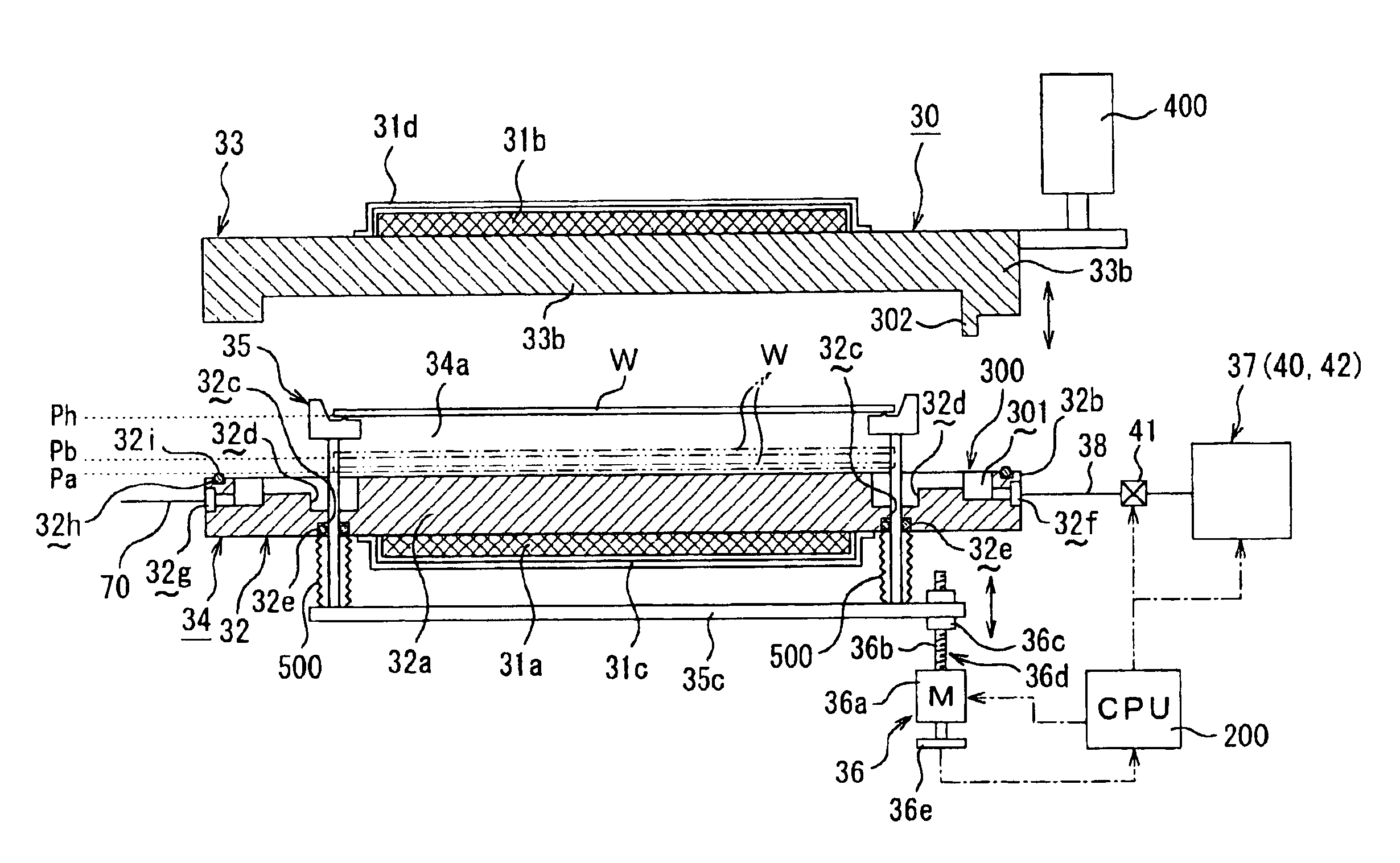
Precise temperature control throughout the wafer reconstitution process is critical for achieving uniform bonding and preventing defects. Advanced thermal management systems monitor and regulate temperature distribution across the wafer surface to minimize thermal gradients and warpage. Temperature ramping rates, dwell times, and cooling profiles are optimized based on material properties and process requirements. Real-time temperature monitoring and feedback control systems ensure consistent processing conditions and high yield.Expand Specific Solutions05 Multi-step temperature profiles for wafer reconstitution
Complex wafer reconstitution processes often employ multi-step temperature profiles with different temperature zones to optimize various stages of the bonding and assembly process. Initial stages may use lower temperatures for alignment and pre-bonding, followed by higher temperatures for final bonding and curing. Intermediate temperature holds allow for stress relaxation and outgassing. The multi-step approach enables better control over material flow, void formation, and final bond quality while accommodating different material requirements in heterogeneous integration.Expand Specific Solutions
Key Players in Semiconductor Wafer Processing Industry
The wafer reconstitution temperature optimization market represents a mature segment within the broader semiconductor manufacturing industry, currently valued at approximately $600 billion globally. The industry is in an advanced consolidation phase, characterized by established technological standards and incremental innovations rather than disruptive breakthroughs. Technology maturity varies significantly across market participants, with equipment leaders like Applied Materials, Tokyo Electron, and Mattson Technology demonstrating advanced thermal processing capabilities through decades of R&D investment. Foundry giants including TSMC, SMIC, and United Microelectronics have achieved high process maturity in temperature-controlled wafer handling. Material suppliers such as Shin-Etsu Handotai, SUMCO, and Siltronic possess sophisticated substrate engineering expertise. However, emerging players like ACM Research and various Chinese manufacturers are rapidly advancing their thermal processing technologies, intensifying competition and driving continued innovation in processing efficiency optimization.
Applied Materials, Inc.
Technical Solution: Applied Materials has developed advanced thermal processing systems for wafer reconstitution that utilize precise temperature control algorithms and multi-zone heating technologies. Their systems feature real-time temperature monitoring with feedback control loops that maintain processing temperatures within ±2°C tolerance. The company's thermal processing equipment incorporates rapid thermal processing (RTP) capabilities with optimized heating profiles that reduce thermal stress during wafer bonding and debonding processes. Their solutions include specialized chuck designs with uniform heat distribution and advanced gas flow management to ensure consistent temperature profiles across the entire wafer surface, significantly improving reconstitution yield rates.
Strengths: Industry-leading thermal control precision and extensive process optimization experience. Weaknesses: High equipment costs and complex system integration requirements.
Tokyo Electron Ltd.
Technical Solution: Tokyo Electron has developed innovative thermal processing solutions for wafer reconstitution featuring their proprietary temperature ramping technology that optimizes heating and cooling cycles. Their systems employ advanced infrared heating with zone-controlled temperature management, enabling precise thermal profiles tailored to different wafer materials and thicknesses. The company's approach includes predictive temperature modeling algorithms that automatically adjust processing parameters based on wafer characteristics and environmental conditions. Their equipment features enhanced thermal uniformity across wafer surfaces through optimized chamber design and gas flow dynamics, resulting in improved reconstitution efficiency and reduced defect rates in advanced packaging applications.
Strengths: Advanced predictive modeling capabilities and excellent thermal uniformity control. Weaknesses: Limited market presence outside Asia and higher maintenance requirements.
Core Thermal Management Innovations in Wafer Processing
Temperature setting method of heat processing plate, temperature setting apparatus of heat processing plate, program, and computer-readable recording medium recording program thereon
PatentActiveUS8874254B2
Innovation
- A temperature setting method for heat processing plates, where a temperature measuring substrate of the same shape as the wafer is used to simulate the wafer's temperature, allowing for real-time temperature adjustments of the plate's regions to ensure uniform heating throughout the processing period, including initial temperature stabilization and reaction periods.


Substrate processing method and apparatus
PatentInactiveUS6954585B2
Innovation
- A substrate processing method and apparatus that involves moving the substrate close to a heating surface to heat it quickly, then moving it away to allow for uniform processing fluid distribution, using a holder and heater mechanism that adjusts position relative to the substrate to ensure efficient heating and fluid supply, and a processing container design that allows for leak-tight processing and uniform fluid diffusion.

Equipment Safety Standards for High-Temperature Wafer Processing
High-temperature wafer processing operations require comprehensive safety frameworks to protect personnel, equipment, and facilities from thermal hazards and associated risks. The semiconductor industry has established rigorous safety protocols specifically addressing temperature-controlled environments where wafer reconstitution processes operate at elevated thermal conditions. These standards encompass multiple layers of protection, from individual operator safety to facility-wide emergency response systems.
Personnel protection standards mandate specialized thermal-resistant personal protective equipment including heat-resistant gloves, face shields, and protective clothing rated for specific temperature ranges. Training protocols require operators to demonstrate competency in thermal hazard recognition, emergency shutdown procedures, and proper handling techniques for high-temperature substrates. Regular certification programs ensure continuous awareness of evolving safety practices and equipment updates.
Equipment design standards specify mandatory safety interlocks that prevent operation beyond predetermined temperature thresholds. Automated monitoring systems must include redundant temperature sensors, emergency cooling mechanisms, and fail-safe shutdown sequences. Thermal isolation requirements dictate minimum clearances between heating elements and operator access points, while ventilation systems must maintain adequate airflow to prevent heat accumulation in work areas.
Facility infrastructure standards address fire suppression systems specifically designed for high-temperature semiconductor processes, including specialized extinguishing agents that do not damage sensitive electronic components. Emergency power systems ensure controlled shutdown capabilities during power failures, preventing thermal shock to processed wafers. Environmental monitoring includes continuous tracking of ambient temperature, humidity levels, and air quality parameters.
Regulatory compliance frameworks integrate international standards from organizations such as SEMI, OSHA, and IEC, establishing baseline requirements for high-temperature processing equipment. Documentation protocols require detailed maintenance logs, temperature calibration records, and incident reporting systems. Regular safety audits and equipment inspections ensure ongoing compliance with evolving industry standards and technological advancements in thermal processing safety.
Energy Efficiency Considerations in Thermal Wafer Processing
Energy efficiency represents a critical consideration in thermal wafer processing, particularly when optimizing processing temperatures for wafer reconstitution. The semiconductor industry faces mounting pressure to reduce energy consumption while maintaining high-quality output, making thermal management strategies essential for sustainable manufacturing operations.
The relationship between processing temperature and energy consumption follows a non-linear pattern in wafer reconstitution processes. Higher temperatures typically require exponentially more energy input due to increased heating requirements and extended cooling cycles. However, optimal temperature ranges often exist where energy efficiency peaks while maintaining acceptable reconstitution quality and throughput rates.
Modern thermal processing systems incorporate advanced energy recovery mechanisms to improve overall efficiency. Heat exchangers capture waste thermal energy from cooling phases and redirect it to preheating incoming wafers, reducing the total energy demand by 15-25%. Additionally, zone-based heating systems allow precise temperature control across different wafer regions, minimizing unnecessary energy expenditure in areas requiring lower thermal input.
Insulation technology plays a pivotal role in energy conservation during thermal processing. Advanced ceramic and aerogel-based insulation materials reduce heat loss by up to 40% compared to traditional insulation methods. These materials maintain thermal barriers while allowing rapid temperature transitions, essential for efficient wafer reconstitution cycles.
Process optimization algorithms increasingly integrate energy consumption metrics alongside quality parameters. Machine learning models analyze historical processing data to identify temperature profiles that minimize energy usage while meeting reconstitution specifications. These systems can reduce energy consumption by 20-30% through intelligent temperature ramping and hold-time optimization.
Emerging technologies such as induction heating and microwave-assisted thermal processing offer promising alternatives to conventional resistive heating methods. These technologies provide more efficient energy transfer mechanisms, reducing processing times and overall energy requirements. Induction heating systems demonstrate up to 50% higher energy efficiency compared to traditional heating elements in specific wafer reconstitution applications.
The implementation of real-time energy monitoring systems enables continuous optimization of thermal processes. These systems track energy consumption patterns and automatically adjust processing parameters to maintain optimal efficiency levels while preserving product quality standards.
Unlock deeper insights with PatSnap Eureka Quick Research — get a full tech report to explore trends and direct your research. Try now!
Generate Your Research Report Instantly with AI Agent
Supercharge your innovation with PatSnap Eureka AI Agent Platform!