

Wafer Reconstitution vs Direct Bonding: Yield Analysis
APR 21, 20269 MIN READ
Generate Your Research Report Instantly with AI Agent
Patsnap Eureka helps you evaluate technical feasibility & market potential.
Wafer Bonding Technology Background and Objectives
Wafer bonding technology has emerged as a critical enabling technology in the semiconductor industry, driven by the relentless pursuit of device miniaturization, enhanced performance, and functional integration. This technology encompasses various methods of joining two or more wafers at the atomic or molecular level to create composite structures that cannot be achieved through conventional single-wafer processing. The evolution of wafer bonding has been particularly accelerated by the demands of advanced packaging, three-dimensional integration, and heterogeneous system integration.
The fundamental principle of wafer bonding involves creating intimate contact between wafer surfaces under controlled conditions of temperature, pressure, and environment. Two primary approaches have gained prominence in industrial applications: wafer reconstitution and direct bonding. Wafer reconstitution involves the assembly of pre-processed die or chiplets onto a carrier substrate, followed by encapsulation and subsequent processing to create a reconstituted wafer format. This approach enables the integration of components from different process nodes and technologies within a single package.
Direct bonding, conversely, involves the permanent joining of complete wafers through various mechanisms including fusion bonding, anodic bonding, or adhesive bonding. This method typically requires pristine wafer surfaces with exceptional flatness and cleanliness to achieve reliable bonds across the entire wafer area. The bonding process often involves thermal treatments that activate chemical bonds between the mating surfaces.
The primary objective of advancing wafer bonding technology centers on achieving maximum yield while maintaining cost-effectiveness and scalability. Yield optimization encompasses multiple dimensions including mechanical integrity, electrical connectivity, thermal management, and long-term reliability. The challenge lies in balancing these requirements while accommodating the inherent variability in wafer properties, process conditions, and material characteristics.
Current industry objectives focus on developing bonding processes that can accommodate increasingly diverse material combinations, including silicon-to-silicon, silicon-to-compound semiconductors, and hybrid organic-inorganic interfaces. The technology must also address the challenges of coefficient of thermal expansion mismatches, stress management, and the preservation of device functionality throughout the bonding process.
The strategic importance of wafer bonding technology extends beyond traditional semiconductor applications into emerging fields such as photonics integration, MEMS devices, and advanced sensor systems. As the industry transitions toward more complex system-in-package and system-on-chip architectures, the ability to reliably bond dissimilar materials and maintain high yields becomes increasingly critical for commercial viability and technological advancement.
Market Demand for Advanced Wafer Processing Solutions
The semiconductor industry is experiencing unprecedented demand for advanced wafer processing solutions, driven by the exponential growth in high-performance computing, artificial intelligence, and mobile device applications. This surge has created significant market pressure for manufacturers to develop more efficient and cost-effective wafer-level packaging technologies that can deliver superior performance while maintaining economic viability.
Traditional packaging approaches are increasingly inadequate for meeting the stringent requirements of next-generation semiconductor devices. The industry faces mounting challenges in achieving higher interconnect density, reduced form factors, and improved electrical performance. These demands have catalyzed substantial market interest in advanced wafer processing techniques, particularly wafer reconstitution and direct bonding methodologies.
The market for advanced wafer processing solutions spans multiple high-growth sectors including data centers, automotive electronics, consumer devices, and telecommunications infrastructure. Each sector presents unique requirements for thermal management, electrical performance, and manufacturing scalability. Data center applications demand exceptional heat dissipation capabilities and signal integrity, while automotive applications prioritize reliability and long-term stability under harsh operating conditions.
Manufacturing yield optimization has emerged as a critical market differentiator, directly impacting profitability and competitive positioning. Companies investing in yield analysis and process optimization technologies are gaining significant advantages in cost structure and time-to-market capabilities. The ability to accurately predict and improve manufacturing yields has become essential for maintaining competitiveness in increasingly price-sensitive markets.
Market dynamics indicate strong preference for solutions that can seamlessly integrate into existing manufacturing infrastructures while delivering measurable improvements in yield performance. Equipment suppliers and process technology developers are responding with innovative approaches that address both technical performance requirements and economic constraints. The convergence of these factors has created substantial market opportunities for companies capable of delivering proven yield enhancement solutions.
The growing complexity of semiconductor devices continues to drive demand for sophisticated process control and yield analysis capabilities. Market participants recognize that sustainable competitive advantage increasingly depends on manufacturing excellence rather than purely technological innovation, positioning advanced wafer processing solutions as strategic investments rather than operational expenses.
Current Challenges in Wafer Reconstitution and Direct Bonding
Wafer reconstitution and direct bonding technologies face significant technical challenges that directly impact manufacturing yield and commercial viability. These challenges stem from the fundamental differences in process complexity, material compatibility requirements, and precision control mechanisms inherent to each approach.
Thermal management represents one of the most critical obstacles in both technologies. During wafer reconstitution, the sequential heating and cooling cycles required for temporary bonding and debonding create thermal stress gradients that can lead to wafer warpage, die shift, and interfacial delamination. The coefficient of thermal expansion mismatch between different materials compounds this issue, particularly when integrating heterogeneous materials such as silicon, gallium arsenide, and various polymer adhesives.
Surface preparation and cleanliness control pose another major challenge category. Direct bonding demands atomically clean surfaces with roughness typically below 0.5 nanometers RMS, requiring sophisticated cleaning protocols and contamination-free environments. Even microscopic particles or organic residues can prevent proper atomic-level bonding, resulting in void formation and reduced bond strength. Wafer reconstitution faces similar cleanliness requirements but additionally must manage adhesive uniformity and thickness control across entire wafer surfaces.
Alignment precision emerges as a fundamental constraint affecting both technologies. Direct bonding requires sub-micron alignment accuracy to maintain electrical connectivity and mechanical integrity, particularly challenging when bonding occurs at elevated temperatures where thermal expansion can cause positional drift. Wafer reconstitution processes must maintain die placement accuracy throughout multiple thermal cycles while managing the mechanical properties of temporary adhesive materials.
Process scalability and throughput limitations significantly impact commercial adoption. Direct bonding typically requires extended processing times for proper interface formation, often involving hours of annealing at elevated temperatures. This creates bottlenecks in high-volume manufacturing environments. Wafer reconstitution, while potentially faster for individual process steps, introduces complexity through multiple handling stages that increase contamination risks and reduce overall equipment effectiveness.
Material compatibility constraints further complicate both approaches. Direct bonding success depends heavily on matching crystal structures, lattice parameters, and thermal properties between bonding partners. Wafer reconstitution must balance temporary adhesive properties with subsequent removal requirements while ensuring compatibility with downstream processing chemicals and temperatures. These material science challenges often require extensive development cycles and limit the range of feasible material combinations for specific applications.
Current Wafer Bonding Solutions and Yield Optimization
01 Wafer bonding interface treatment and surface preparation methods
Surface preparation techniques are critical for achieving high bonding yield in wafer reconstitution. Methods include plasma treatment, chemical mechanical polishing, and surface activation to ensure proper adhesion between bonded surfaces. Surface roughness control and contamination removal are essential steps to minimize defects at the bonding interface. Proper surface energy matching and hydrophilic treatment can significantly improve direct bonding quality and reduce void formation.- Wafer bonding interface treatment and surface preparation methods: Surface preparation techniques are critical for achieving high bonding yield in wafer reconstitution. Methods include plasma treatment, chemical mechanical polishing, and surface activation to ensure proper adhesion between bonded wafers. Surface roughness control and contamination removal are essential steps to minimize defects at the bonding interface. Proper cleaning and activation processes can significantly improve the direct bonding quality and reduce void formation.
- Alignment and positioning control in wafer bonding processes: Precise alignment and positioning systems are crucial for maintaining high yield in wafer reconstitution and direct bonding. Advanced alignment techniques using optical recognition, infrared imaging, and mechanical fixtures ensure accurate wafer-to-wafer registration. Misalignment detection and correction mechanisms help prevent bonding failures and improve overall process yield. Real-time monitoring systems enable immediate adjustments during the bonding process.
- Temperature and pressure control during bonding: Optimized temperature and pressure profiles are essential for successful wafer bonding and high yield. Controlled heating and cooling cycles prevent thermal stress and warpage in bonded wafer structures. Pressure distribution uniformity across the bonding interface ensures consistent bond strength. Process parameters must be carefully tuned based on wafer materials and thickness to achieve optimal bonding results.
- Defect detection and yield monitoring techniques: Advanced inspection methods are employed to detect bonding defects and monitor yield in wafer reconstitution processes. Acoustic microscopy, infrared imaging, and optical inspection systems identify voids, delamination, and other bonding failures. Statistical process control and real-time monitoring enable early detection of yield issues. Automated defect classification systems help optimize process parameters and improve overall bonding quality.
- Reconstituted wafer handling and post-bonding processes: Specialized handling techniques and post-bonding treatments are necessary to maintain yield in reconstituted wafers. Stress relief annealing and controlled cooling prevent wafer warpage and cracking. Thinning and planarization processes ensure uniform thickness across the bonded structure. Proper handling fixtures and transport systems minimize mechanical damage to fragile bonded wafer assemblies during subsequent processing steps.
02 Alignment and positioning accuracy in wafer bonding processes
Precise alignment systems and positioning mechanisms are crucial for maintaining high yield in direct wafer bonding. Advanced alignment techniques using infrared imaging, pattern recognition, and real-time feedback control ensure accurate overlay between wafers. Mechanical fixtures and vacuum chucks help maintain positional stability during the bonding process. Automated alignment systems can achieve sub-micron accuracy, which is essential for high-density interconnect applications.Expand Specific Solutions03 Thermal management and annealing processes for bonded wafers
Controlled thermal treatment is essential for strengthening bonded interfaces and improving yield. Annealing processes at specific temperatures and durations enhance bond strength by promoting atomic diffusion and eliminating interfacial voids. Temperature ramping profiles and uniform heating distribution prevent thermal stress and wafer warpage. Optimized thermal cycles can significantly reduce debonding risks and improve the mechanical integrity of reconstituted wafers.Expand Specific Solutions04 Defect detection and quality inspection methods
Non-destructive testing techniques are employed to identify bonding defects and ensure high yield. Acoustic microscopy, infrared imaging, and optical inspection systems can detect voids, delamination, and particle contamination at bonding interfaces. Automated inspection systems enable rapid screening of bonded wafer pairs to identify defective units. Statistical process control and real-time monitoring help optimize bonding parameters and maintain consistent quality.Expand Specific Solutions05 Temporary bonding and debonding techniques for wafer reconstitution
Temporary bonding materials and processes enable handling of thinned wafers during reconstitution while maintaining high yield. Polymer-based adhesives and thermal release tapes provide sufficient bonding strength for processing while allowing clean debonding without residue. Controlled debonding processes using thermal, mechanical, or laser-assisted methods minimize wafer damage and stress. Proper selection of temporary bonding materials based on process temperature requirements ensures compatibility with subsequent manufacturing steps.Expand Specific Solutions
Key Players in Wafer Processing and Bonding Equipment
The wafer reconstitution versus direct bonding technology landscape represents a rapidly evolving segment within advanced semiconductor packaging, currently in the growth phase with significant market expansion driven by 3D IC integration demands. The global market is experiencing robust growth as manufacturers seek higher integration density and improved performance. Technology maturity varies significantly across players, with established foundries like Taiwan Semiconductor Manufacturing Co. and Semiconductor Manufacturing International Corp. leading in direct bonding capabilities, while specialized companies such as Invensas Bonding Technologies and Soitec SA drive innovation in reconstitution techniques. Chinese players including Yangtze Memory Technologies and Wuhan Xinxin Semiconductor are rapidly advancing their capabilities, while equipment suppliers like Tokyo Electron and SUSS MicroTec provide critical manufacturing infrastructure, creating a competitive ecosystem where yield optimization remains the primary differentiator.
Taiwan Semiconductor Manufacturing Co., Ltd.
Technical Solution: TSMC has developed advanced wafer-level packaging technologies including CoWoS (Chip on Wafer on Substrate) and InFO (Integrated Fan-Out) that utilize both wafer reconstitution and direct bonding approaches. Their CoWoS technology employs silicon interposers with through-silicon vias (TSVs) for high-density interconnections, achieving yields above 95% for complex multi-die packages. The InFO technology uses wafer reconstitution processes where dies are embedded in molding compound and reconstituted into wafer form for subsequent processing, enabling fine-pitch redistribution layers with yields exceeding 90%. TSMC's direct bonding capabilities include hybrid bonding for memory applications, combining copper-to-copper and dielectric-to-dielectric bonding with alignment accuracy better than 1μm.
Strengths: Industry-leading yield rates, mature process control, extensive experience in high-volume manufacturing. Weaknesses: High capital investment requirements, complex process integration challenges for new applications.
Invensas Bonding Technologies, Inc.
Technical Solution: Invensas specializes in ZiBond and DBI (Direct Bond Interconnect) technologies for advanced packaging applications. Their ZiBond process enables room-temperature bonding of oxide surfaces followed by low-temperature annealing, achieving bond strengths comparable to fusion bonding while maintaining high yields above 98% for wafer-to-wafer applications. The DBI technology combines dielectric bonding with fine-pitch copper interconnects, enabling direct electrical connections without traditional solder bumps. Their wafer reconstitution approach uses temporary carrier wafers with specialized release layers, allowing processing of ultra-thin dies with thickness down to 25μm while maintaining structural integrity throughout the manufacturing process.
Strengths: Innovative low-temperature bonding processes, excellent for heterogeneous integration, strong IP portfolio. Weaknesses: Limited high-volume manufacturing experience compared to traditional foundries, newer technology with less market validation.
Core Yield Enhancement Patents in Wafer Bonding
Method for Producing Direct Bonded Wafer and Direct Bonded Wafer
PatentInactiveUS20080102603A1
Innovation
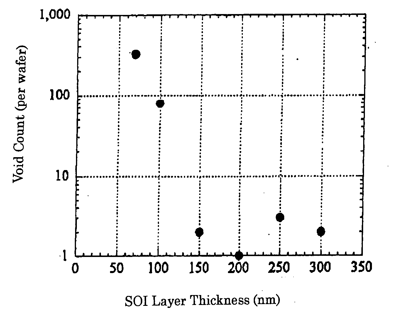
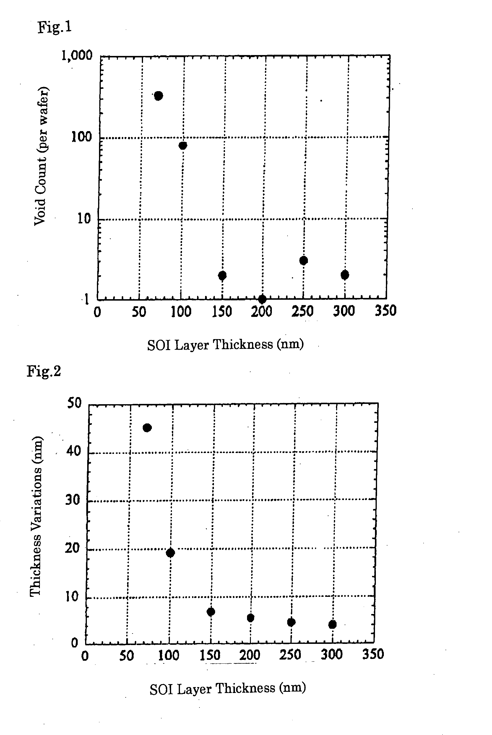
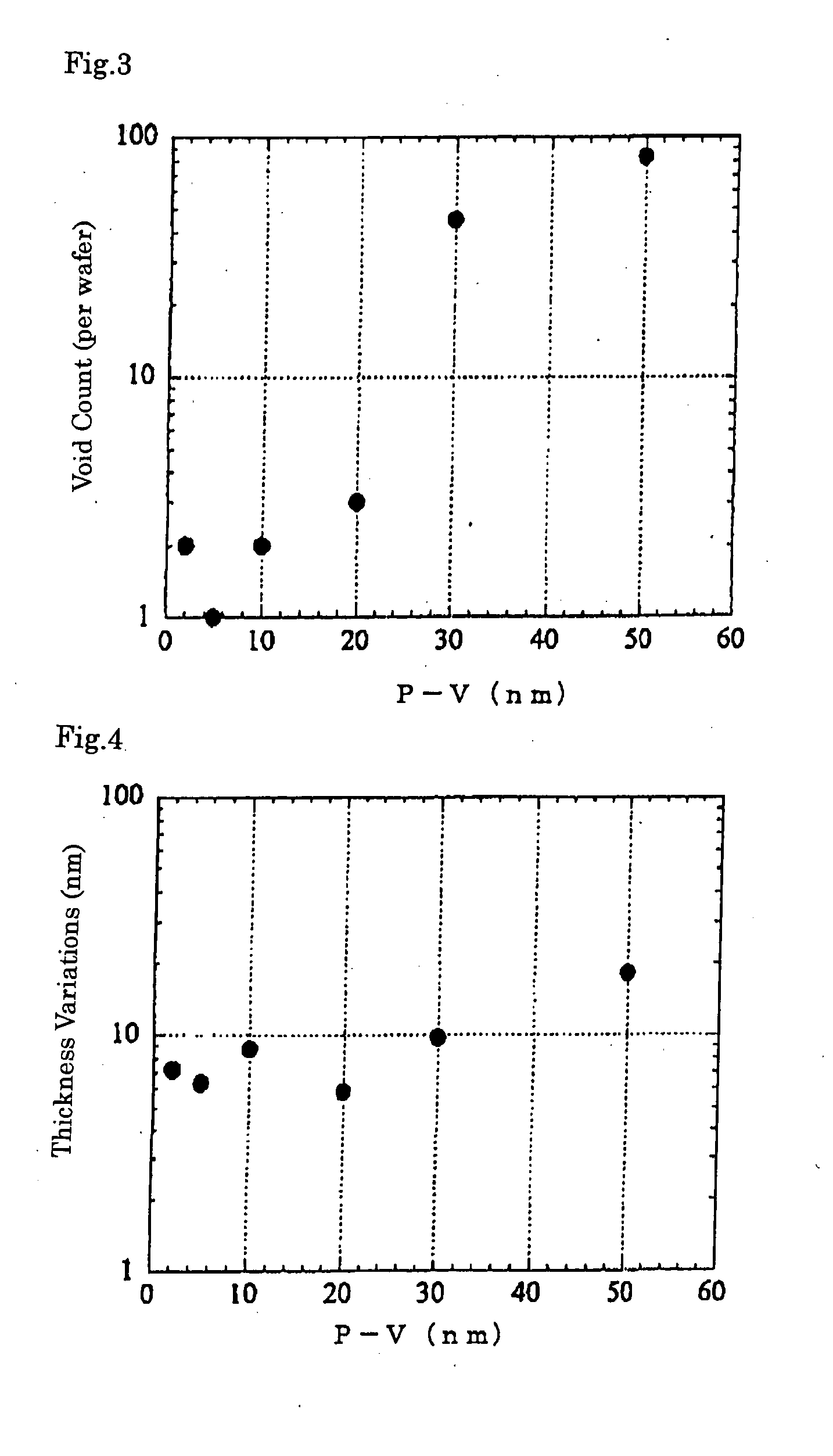
- A method involving the formation of a thermal or CVD oxide film on at least one wafer, bonding via the oxide film, thinning the bond wafer, and subsequent annealing in an inert or hydrogen atmosphere to remove the oxide film, allowing direct bonding and reducing voids.

Direct bonding methods and structures
PatentActiveUS20230140107A1
Innovation
- A method involving slight etching with liquid etchants like hydrofluoric acid and terminating treatments with species such as tetramethylammonium hydroxide or boron-containing solutions to directly bond nonconductive field regions without plasma exposure, enabling strong adhesive-free bonds at room temperature with subsequent annealing for enhanced strength.


Semiconductor Manufacturing Quality Standards
Semiconductor manufacturing quality standards for wafer reconstitution and direct bonding processes are governed by stringent international frameworks that ensure consistent yield performance and product reliability. The primary standards include SEMI specifications, IPC guidelines, and ISO 9001 quality management systems, which collectively establish baseline requirements for process control, material handling, and defect management in advanced packaging applications.
Quality control metrics for wafer reconstitution processes focus on adhesive uniformity, die placement accuracy, and thermal cycling reliability. Industry standards mandate die shear strength values exceeding 10 kg-force, with coefficient of variation below 15% across the reconstituted wafer surface. Temperature cycling requirements typically specify 1000 cycles between -55°C and 125°C without delamination or electrical failure, ensuring long-term reliability in automotive and aerospace applications.
Direct bonding quality standards emphasize surface preparation, bonding energy thresholds, and interfacial void density measurements. SEMI M77 guidelines specify surface roughness parameters below 0.5nm RMS for successful Cu-Cu thermocompression bonding, while oxide-oxide fusion bonding requires hydrophilic surface treatments with contact angles less than 10 degrees. Void density specifications typically limit interfacial defects to less than 0.1% of the total bonding area.
Statistical process control implementation requires real-time monitoring of critical parameters including bonding force, temperature uniformity, and alignment accuracy. Six Sigma methodologies are commonly employed to achieve defect rates below 3.4 parts per million, with control charts tracking process capability indices (Cpk) above 1.33 for key quality characteristics.
Traceability standards mandate comprehensive documentation of material lots, process parameters, and inspection results throughout the manufacturing flow. Electronic data management systems must maintain audit trails compliant with FDA 21 CFR Part 11 requirements for medical device applications, while automotive standards require PPAP documentation demonstrating process capability and long-term stability.
Yield calculation methodologies follow standardized definitions where electrical yield represents functional die percentage after final test, while mechanical yield accounts for structural integrity after assembly processes. Industry benchmarks typically target electrical yields above 95% for mature processes, with continuous improvement programs focusing on defect source identification and elimination through advanced statistical analysis techniques.
Cost-Benefit Analysis of Bonding Technologies
The economic evaluation of wafer reconstitution versus direct bonding technologies reveals significant differences in capital expenditure requirements and operational cost structures. Direct bonding typically demands higher initial investment due to sophisticated alignment systems, precision temperature control equipment, and specialized surface preparation tools. The equipment costs for direct bonding can exceed $5-8 million per production line, while wafer reconstitution systems generally require $3-5 million in initial capital outlay.
Operational expenditures present contrasting profiles between these technologies. Wafer reconstitution involves additional material costs for temporary carriers, adhesives, and debonding processes, contributing to approximately 15-20% higher consumable expenses per wafer processed. However, direct bonding eliminates these material requirements while introducing elevated energy consumption due to high-temperature processing and extended cycle times.
Labor costs favor direct bonding in high-volume production scenarios, as the process requires fewer manual intervention steps and reduces handling complexity. The automation potential of direct bonding translates to 25-30% lower labor costs per unit in mature production environments. Conversely, wafer reconstitution demands more intensive process monitoring and carrier management, increasing operational overhead.
Yield-related financial impacts significantly influence the cost-benefit equation. Direct bonding's superior yield performance, typically achieving 95-98% compared to reconstitution's 85-92%, generates substantial cost savings through reduced material waste and rework expenses. The improved yield translates to approximately $200-400 cost reduction per processed wafer in high-value applications.
Time-to-market considerations add another economic dimension, where direct bonding's streamlined process flow can accelerate product development cycles by 20-30%, providing competitive advantages that often justify higher initial investments. The total cost of ownership analysis typically favors direct bonding for high-volume, high-value applications, while wafer reconstitution remains economically viable for prototyping and specialized low-volume production scenarios.
Unlock deeper insights with Patsnap Eureka Quick Research — get a full tech report to explore trends and direct your research. Try now!
Generate Your Research Report Instantly with AI Agent
Supercharge your innovation with Patsnap Eureka AI Agent Platform!