

Optimize Wafer Inspection Algorithms to Improve Defect Identification
MAY 19, 20269 MIN READ
Generate Your Research Report Instantly with AI Agent
Patsnap Eureka helps you evaluate technical feasibility & market potential.
Wafer Inspection Algorithm Background and Objectives
Wafer inspection has evolved as a critical component of semiconductor manufacturing since the early days of integrated circuit production in the 1960s. Initially, visual inspection methods dominated the field, relying heavily on human operators to identify surface defects and contamination. As semiconductor devices became increasingly miniaturized and complex, the limitations of manual inspection became apparent, driving the industry toward automated optical inspection systems in the 1980s.
The transition from rule-based inspection algorithms to advanced machine learning approaches represents a significant paradigm shift in wafer inspection technology. Early automated systems utilized simple pattern matching and threshold-based detection methods, which proved inadequate for identifying subtle defects in modern nanoscale manufacturing processes. The introduction of statistical process control and image processing algorithms in the 1990s marked the beginning of more sophisticated defect detection capabilities.
Contemporary wafer inspection faces unprecedented challenges due to the continuous scaling of semiconductor devices below 10nm technology nodes. Traditional inspection algorithms struggle with increased noise levels, reduced signal-to-noise ratios, and the growing complexity of three-dimensional device structures. The emergence of new materials, advanced packaging technologies, and heterogeneous integration further complicates defect identification processes.
Current technological trends indicate a strong movement toward artificial intelligence and deep learning-based inspection algorithms. Convolutional neural networks, computer vision techniques, and advanced signal processing methods are being integrated to enhance defect detection sensitivity and reduce false positive rates. The industry is also exploring multi-modal inspection approaches that combine optical, electron beam, and X-ray imaging technologies.
The primary objective of optimizing wafer inspection algorithms centers on achieving higher defect detection accuracy while maintaining throughput requirements essential for high-volume manufacturing. This involves developing algorithms capable of identifying defects smaller than 10nm with detection rates exceeding 95% and false alarm rates below 1%. Additionally, the algorithms must adapt to process variations and new defect types without extensive retraining.
Future algorithmic development aims to establish predictive inspection capabilities that can anticipate potential defect formation based on process parameters and historical data patterns. The integration of real-time feedback mechanisms and adaptive learning systems represents the next frontier in wafer inspection technology evolution.
The transition from rule-based inspection algorithms to advanced machine learning approaches represents a significant paradigm shift in wafer inspection technology. Early automated systems utilized simple pattern matching and threshold-based detection methods, which proved inadequate for identifying subtle defects in modern nanoscale manufacturing processes. The introduction of statistical process control and image processing algorithms in the 1990s marked the beginning of more sophisticated defect detection capabilities.
Contemporary wafer inspection faces unprecedented challenges due to the continuous scaling of semiconductor devices below 10nm technology nodes. Traditional inspection algorithms struggle with increased noise levels, reduced signal-to-noise ratios, and the growing complexity of three-dimensional device structures. The emergence of new materials, advanced packaging technologies, and heterogeneous integration further complicates defect identification processes.
Current technological trends indicate a strong movement toward artificial intelligence and deep learning-based inspection algorithms. Convolutional neural networks, computer vision techniques, and advanced signal processing methods are being integrated to enhance defect detection sensitivity and reduce false positive rates. The industry is also exploring multi-modal inspection approaches that combine optical, electron beam, and X-ray imaging technologies.
The primary objective of optimizing wafer inspection algorithms centers on achieving higher defect detection accuracy while maintaining throughput requirements essential for high-volume manufacturing. This involves developing algorithms capable of identifying defects smaller than 10nm with detection rates exceeding 95% and false alarm rates below 1%. Additionally, the algorithms must adapt to process variations and new defect types without extensive retraining.
Future algorithmic development aims to establish predictive inspection capabilities that can anticipate potential defect formation based on process parameters and historical data patterns. The integration of real-time feedback mechanisms and adaptive learning systems represents the next frontier in wafer inspection technology evolution.
Market Demand for Advanced Semiconductor Defect Detection
The global semiconductor industry faces unprecedented pressure to enhance manufacturing yield and product reliability as device geometries continue to shrink and circuit complexity increases. Advanced wafer inspection technologies have become critical enablers for maintaining competitive advantage in semiconductor fabrication, driving substantial market demand across multiple industry segments.
The automotive electronics sector represents one of the fastest-growing demand drivers for enhanced defect detection capabilities. As vehicles integrate more sophisticated electronic systems including autonomous driving features, advanced driver assistance systems, and electric powertrains, the reliability requirements for automotive semiconductors have intensified significantly. Zero-defect manufacturing has become essential, as semiconductor failures in safety-critical automotive applications can have catastrophic consequences.
Consumer electronics manufacturers continue to push for higher performance and miniaturization, creating additional market pressure for improved inspection algorithms. The proliferation of 5G devices, artificial intelligence processors, and high-resolution display technologies requires semiconductor components with increasingly tight tolerance specifications. Traditional inspection methods struggle to detect subtle defects that can compromise device performance in these demanding applications.
Data center and cloud computing infrastructure expansion has generated substantial demand for high-performance processors and memory devices. These applications require exceptional reliability and performance consistency, driving semiconductor manufacturers to invest heavily in advanced inspection technologies. The economic impact of defective components in data center environments creates strong incentives for comprehensive defect detection during manufacturing.
The Internet of Things ecosystem presents unique challenges for semiconductor defect detection, as IoT devices often operate in harsh environments with limited maintenance opportunities. This market segment demands robust semiconductor components with extended operational lifespans, necessitating more sophisticated inspection algorithms capable of identifying potential reliability issues during manufacturing.
Emerging technologies including quantum computing, neuromorphic processors, and advanced photonic devices are creating new categories of defects that traditional inspection methods cannot adequately address. These next-generation applications require novel inspection approaches and algorithm optimization techniques, representing significant market opportunities for companies developing advanced defect detection solutions.
Market dynamics indicate strong growth potential across all semiconductor application segments, with particular emphasis on inspection technologies that can adapt to evolving manufacturing processes and emerging defect types. The convergence of artificial intelligence, machine learning, and traditional optical inspection methods is reshaping market expectations and creating new competitive landscapes in semiconductor manufacturing quality assurance.
The automotive electronics sector represents one of the fastest-growing demand drivers for enhanced defect detection capabilities. As vehicles integrate more sophisticated electronic systems including autonomous driving features, advanced driver assistance systems, and electric powertrains, the reliability requirements for automotive semiconductors have intensified significantly. Zero-defect manufacturing has become essential, as semiconductor failures in safety-critical automotive applications can have catastrophic consequences.
Consumer electronics manufacturers continue to push for higher performance and miniaturization, creating additional market pressure for improved inspection algorithms. The proliferation of 5G devices, artificial intelligence processors, and high-resolution display technologies requires semiconductor components with increasingly tight tolerance specifications. Traditional inspection methods struggle to detect subtle defects that can compromise device performance in these demanding applications.
Data center and cloud computing infrastructure expansion has generated substantial demand for high-performance processors and memory devices. These applications require exceptional reliability and performance consistency, driving semiconductor manufacturers to invest heavily in advanced inspection technologies. The economic impact of defective components in data center environments creates strong incentives for comprehensive defect detection during manufacturing.
The Internet of Things ecosystem presents unique challenges for semiconductor defect detection, as IoT devices often operate in harsh environments with limited maintenance opportunities. This market segment demands robust semiconductor components with extended operational lifespans, necessitating more sophisticated inspection algorithms capable of identifying potential reliability issues during manufacturing.
Emerging technologies including quantum computing, neuromorphic processors, and advanced photonic devices are creating new categories of defects that traditional inspection methods cannot adequately address. These next-generation applications require novel inspection approaches and algorithm optimization techniques, representing significant market opportunities for companies developing advanced defect detection solutions.
Market dynamics indicate strong growth potential across all semiconductor application segments, with particular emphasis on inspection technologies that can adapt to evolving manufacturing processes and emerging defect types. The convergence of artificial intelligence, machine learning, and traditional optical inspection methods is reshaping market expectations and creating new competitive landscapes in semiconductor manufacturing quality assurance.
Current State and Challenges in Wafer Inspection Algorithms
Wafer inspection algorithms have evolved significantly over the past two decades, transitioning from traditional rule-based systems to sophisticated machine learning approaches. Current mainstream technologies primarily rely on optical inspection systems combined with advanced image processing algorithms, including convolutional neural networks (CNNs), support vector machines (SVMs), and hybrid detection frameworks. These systems typically operate at nanometer-scale resolution requirements, processing thousands of images per wafer within stringent throughput constraints.
The semiconductor industry currently employs multiple algorithmic approaches for defect detection, ranging from pattern matching and statistical process control methods to deep learning-based classification systems. Leading inspection platforms integrate multi-modal sensing technologies, combining brightfield, darkfield, and electron beam inspection capabilities. However, these systems face increasing complexity as semiconductor nodes shrink below 7nm, where traditional optical limitations become more pronounced.
Contemporary wafer inspection faces several critical technical challenges that significantly impact defect identification accuracy and operational efficiency. False positive rates remain problematically high, often exceeding 80% in advanced node production, leading to substantial productivity losses and increased review costs. The algorithms struggle particularly with nuisance defects, which are detected anomalies that do not affect device functionality but consume valuable inspection and review resources.
Algorithm sensitivity and specificity present ongoing optimization challenges, especially when dealing with process-induced variations and systematic defects. Current systems often require extensive parameter tuning for different product types and manufacturing processes, limiting their adaptability and scalability across diverse production environments. The trade-off between detection sensitivity and throughput continues to constrain real-time inspection capabilities.
Emerging defect types associated with advanced materials and three-dimensional device structures pose additional algorithmic challenges. Traditional two-dimensional inspection approaches prove insufficient for detecting subsurface defects, interface anomalies, and complex three-dimensional structural variations. The increasing diversity of defect morphologies requires more sophisticated pattern recognition capabilities than current algorithms typically provide.
Data quality and training dataset limitations further constrain algorithm performance improvements. Insufficient labeled defect samples, particularly for rare but critical defect types, hinder machine learning model development and validation. The dynamic nature of semiconductor manufacturing processes creates continuous algorithm drift, requiring frequent recalibration and model updates to maintain optimal performance levels across varying production conditions.
The semiconductor industry currently employs multiple algorithmic approaches for defect detection, ranging from pattern matching and statistical process control methods to deep learning-based classification systems. Leading inspection platforms integrate multi-modal sensing technologies, combining brightfield, darkfield, and electron beam inspection capabilities. However, these systems face increasing complexity as semiconductor nodes shrink below 7nm, where traditional optical limitations become more pronounced.
Contemporary wafer inspection faces several critical technical challenges that significantly impact defect identification accuracy and operational efficiency. False positive rates remain problematically high, often exceeding 80% in advanced node production, leading to substantial productivity losses and increased review costs. The algorithms struggle particularly with nuisance defects, which are detected anomalies that do not affect device functionality but consume valuable inspection and review resources.
Algorithm sensitivity and specificity present ongoing optimization challenges, especially when dealing with process-induced variations and systematic defects. Current systems often require extensive parameter tuning for different product types and manufacturing processes, limiting their adaptability and scalability across diverse production environments. The trade-off between detection sensitivity and throughput continues to constrain real-time inspection capabilities.
Emerging defect types associated with advanced materials and three-dimensional device structures pose additional algorithmic challenges. Traditional two-dimensional inspection approaches prove insufficient for detecting subsurface defects, interface anomalies, and complex three-dimensional structural variations. The increasing diversity of defect morphologies requires more sophisticated pattern recognition capabilities than current algorithms typically provide.
Data quality and training dataset limitations further constrain algorithm performance improvements. Insufficient labeled defect samples, particularly for rare but critical defect types, hinder machine learning model development and validation. The dynamic nature of semiconductor manufacturing processes creates continuous algorithm drift, requiring frequent recalibration and model updates to maintain optimal performance levels across varying production conditions.
Existing Algorithmic Solutions for Wafer Defect Identification
01 Machine learning and AI-based defect detection algorithms
Advanced machine learning techniques and artificial intelligence algorithms are employed to automatically identify and classify defects on wafer surfaces. These methods utilize neural networks, deep learning models, and pattern recognition systems to analyze inspection data and distinguish between normal surface features and actual defects. The algorithms are trained on large datasets to improve accuracy and reduce false positive rates in defect identification.- Machine learning and AI-based defect detection algorithms: Advanced machine learning techniques and artificial intelligence algorithms are employed to automatically identify and classify defects on wafer surfaces. These methods utilize neural networks, deep learning models, and pattern recognition systems to analyze inspection images and detect anomalies with high accuracy and speed. The algorithms can be trained on large datasets to improve detection capabilities and reduce false positives.
- Optical inspection systems and image processing techniques: Sophisticated optical inspection systems combined with advanced image processing algorithms are used to capture and analyze high-resolution images of wafer surfaces. These systems employ various lighting conditions, camera configurations, and image enhancement techniques to detect surface defects, particles, and structural anomalies. The processing algorithms include filtering, edge detection, and contrast enhancement methods.
- Statistical analysis and threshold-based detection methods: Statistical approaches and threshold-based algorithms are implemented to identify defects by comparing measured parameters against predetermined standards. These methods analyze statistical variations in wafer properties, establish baseline measurements, and flag deviations that exceed acceptable limits. The algorithms incorporate statistical process control and variance analysis techniques.
- Multi-sensor fusion and comprehensive inspection algorithms: Integration of multiple sensing technologies and inspection methods creates comprehensive defect identification systems. These algorithms combine data from various sensors including optical, electrical, and mechanical measurement devices to provide complete wafer analysis. The fusion approach enhances detection accuracy by correlating information from different inspection modalities.
- Real-time processing and automated classification systems: High-speed processing algorithms enable real-time defect detection and automated classification during wafer inspection processes. These systems implement parallel processing techniques, optimized computational methods, and automated decision-making algorithms to maintain production throughput while ensuring quality control. The algorithms can categorize defects by type, severity, and location for process optimization.
02 Image processing and optical inspection techniques
Sophisticated image processing algorithms are used to analyze optical images captured during wafer inspection. These techniques involve edge detection, contrast enhancement, filtering methods, and morphological operations to identify surface anomalies and defects. The algorithms process high-resolution images to detect minute defects that could affect semiconductor device performance.Expand Specific Solutions03 Statistical analysis and threshold-based detection methods
Statistical algorithms analyze measurement data and establish threshold values to identify deviations from normal wafer characteristics. These methods use statistical process control techniques, variance analysis, and probability distributions to determine when measurements indicate the presence of defects. The algorithms continuously update thresholds based on process variations and historical data.Expand Specific Solutions04 Multi-sensor data fusion and correlation algorithms
Advanced algorithms combine data from multiple inspection sensors and measurement tools to provide comprehensive defect identification. These methods correlate information from different inspection modalities, such as optical, electrical, and physical measurements, to improve detection accuracy and reduce inspection time. The fusion algorithms weight different sensor inputs based on their reliability and relevance to specific defect types.Expand Specific Solutions05 Real-time processing and adaptive inspection algorithms
Real-time algorithms enable immediate defect detection during wafer processing, allowing for quick feedback and process adjustments. These adaptive systems modify inspection parameters and detection criteria based on ongoing process conditions and defect patterns. The algorithms optimize inspection speed while maintaining high detection sensitivity for critical defects.Expand Specific Solutions
Key Players in Semiconductor Inspection Equipment Industry
The wafer inspection algorithm optimization market is experiencing rapid growth driven by increasing semiconductor complexity and miniaturization demands. The industry is in a mature expansion phase with significant market opportunities, as evidenced by the diverse ecosystem of established players and emerging specialists. Technology maturity varies significantly across market segments, with established equipment manufacturers like Applied Materials, KLA Corp, Tokyo Electron, and Hitachi demonstrating advanced capabilities in traditional inspection systems. Meanwhile, specialized companies such as Camtek, Unity Semiconductor, and Skyverse Technology are driving innovation in AI-enhanced defect detection algorithms. Major semiconductor manufacturers including TSMC, Samsung Electronics, and foundries like United Microelectronics are simultaneously developing proprietary inspection solutions, creating a competitive landscape where equipment suppliers, chip manufacturers, and specialized software companies are converging to address increasingly sophisticated defect identification challenges in advanced node production.
Samsung Electronics Co., Ltd.
Technical Solution: Samsung develops custom deep learning algorithms optimized for memory device inspection, particularly focusing on 3D NAND and advanced DRAM structures. Their inspection algorithms utilize transformer-based neural networks to analyze complex three-dimensional defect patterns that traditional 2D inspection methods cannot effectively detect. The company's approach includes multi-modal inspection combining electrical testing data with optical inspection results to improve defect identification accuracy. Samsung's algorithms incorporate transfer learning techniques to quickly adapt to new product designs and process variations. Their system features automated defect severity assessment that prioritizes critical defects affecting device reliability and performance, enabling efficient quality control in high-volume production environments.
Strengths: Specialized expertise in memory device defects with advanced 3D inspection capabilities. Weaknesses: Algorithms are primarily optimized for memory products and may require significant modification for logic devices.
KLA Corp.
Technical Solution: KLA develops advanced machine learning algorithms integrated with their inspection systems to enhance defect detection accuracy. Their technology combines deep learning neural networks with traditional image processing techniques to identify subtle defects that conventional methods might miss. The company's algorithms utilize multi-spectral imaging and pattern recognition to distinguish between actual defects and process variations. Their inspection systems can process thousands of wafers per hour while maintaining high sensitivity to critical defects. KLA's algorithms are continuously trained on large datasets from various semiconductor processes to improve detection rates and reduce false positives across different technology nodes.
Strengths: Industry-leading detection accuracy and processing speed, extensive database for algorithm training. Weaknesses: High system cost and complexity requiring specialized maintenance expertise.
Core Innovations in AI-Based Defect Detection Algorithms
Defect discovery and inspection sensitivity optimization using automated classification of corresponding electron beam images
PatentActiveTW201531698A
Innovation
- A computer-implemented method and system that automatically classify defects using electron beam images, determining defect classification without user input, and integrating with wafer inspection tools to enhance sensitivity and accuracy.


Method, apparatus, and computer program product for optimizing inspection recipes using programmed defects
PatentInactiveUS7397556B2
Innovation
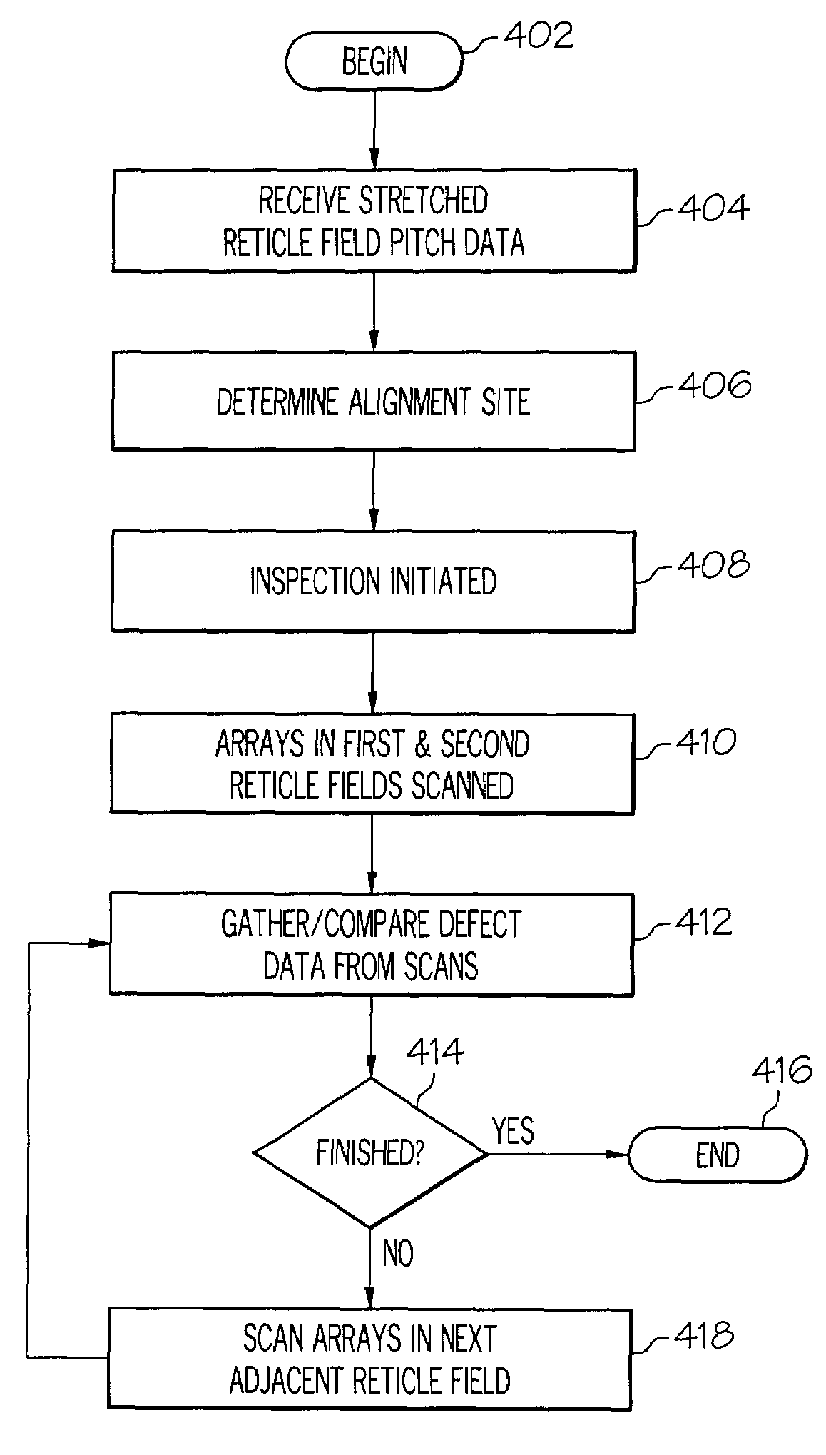
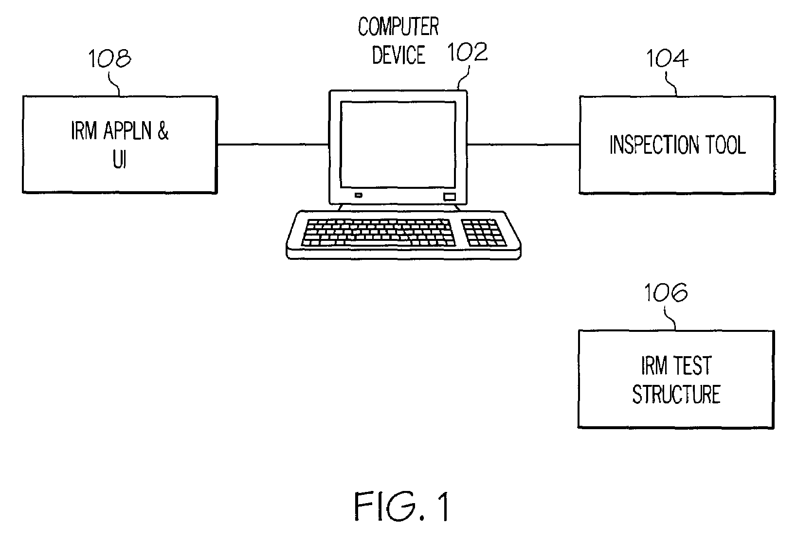
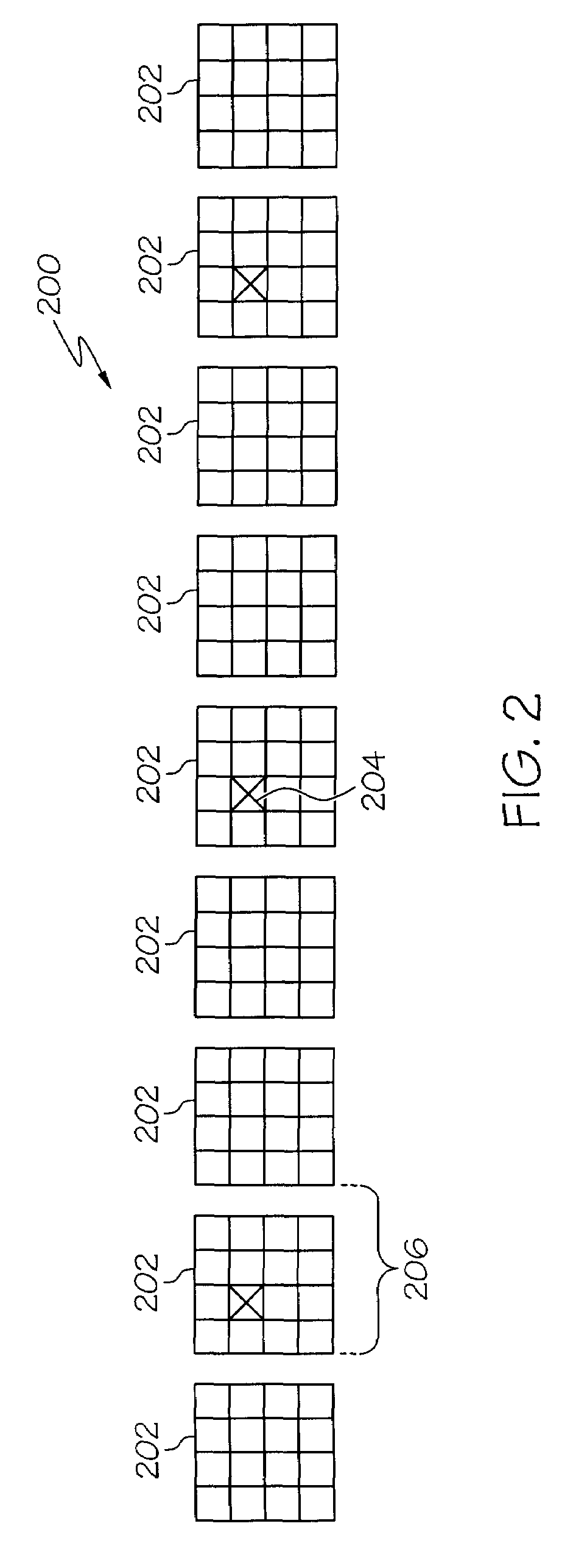
- A test structure with arrays spaced equidistantly on a semiconductor substrate, where every third array contains a programmed defect, and a modified reticle pitch extending one reticle field plus an adjacent field, allows for random mode inspection using a 'stretched reticle field pitch' to optimize inspection tool sensitivity effectively.

Semiconductor Manufacturing Quality Standards and Compliance
Semiconductor manufacturing quality standards serve as the foundational framework governing wafer inspection processes and defect identification protocols. The International Technology Roadmap for Semiconductors (ITRS) and its successor, the International Roadmap for Devices and Systems (IRDS), establish critical benchmarks for defect density limits, typically requiring less than 0.1 defects per square centimeter for advanced nodes below 7nm. These standards directly influence the sensitivity requirements and performance metrics that optimized inspection algorithms must achieve.
ISO 9001 quality management systems and semiconductor-specific standards like SEMI E10 for equipment automation provide structured approaches to implementing algorithmic improvements within existing manufacturing workflows. Compliance with these standards ensures that enhanced defect identification capabilities integrate seamlessly with established quality control processes while maintaining traceability and documentation requirements essential for regulatory approval.
The Automotive Electronics Council (AEC) standards, particularly AEC-Q100 for integrated circuits, impose stringent defect detection requirements that drive algorithm optimization toward zero-defect manufacturing goals. These automotive-grade specifications demand detection capabilities for defects as small as 10-20 nanometers, pushing inspection algorithms to achieve unprecedented sensitivity levels while maintaining acceptable false positive rates below 5%.
FDA regulations for medical device semiconductors and aerospace industry standards such as AS9100 establish additional compliance layers that influence algorithm development priorities. These regulations emphasize statistical process control and require inspection systems to demonstrate consistent performance across extended operational periods, necessitating robust algorithmic approaches that maintain accuracy under varying environmental conditions.
Environmental compliance standards including RoHS and REACH regulations impact the selection of materials and processes used in wafer fabrication, which subsequently affects the types of defects that inspection algorithms must identify. Algorithm optimization must account for new defect signatures emerging from lead-free soldering processes and alternative materials mandated by environmental regulations.
Quality standards also define acceptable sampling rates and inspection coverage requirements, with many specifications demanding 100% wafer inspection for critical applications. This comprehensive coverage requirement drives the need for high-throughput algorithmic solutions capable of processing entire wafer surfaces within manufacturing cycle time constraints while maintaining detection accuracy standards.
ISO 9001 quality management systems and semiconductor-specific standards like SEMI E10 for equipment automation provide structured approaches to implementing algorithmic improvements within existing manufacturing workflows. Compliance with these standards ensures that enhanced defect identification capabilities integrate seamlessly with established quality control processes while maintaining traceability and documentation requirements essential for regulatory approval.
The Automotive Electronics Council (AEC) standards, particularly AEC-Q100 for integrated circuits, impose stringent defect detection requirements that drive algorithm optimization toward zero-defect manufacturing goals. These automotive-grade specifications demand detection capabilities for defects as small as 10-20 nanometers, pushing inspection algorithms to achieve unprecedented sensitivity levels while maintaining acceptable false positive rates below 5%.
FDA regulations for medical device semiconductors and aerospace industry standards such as AS9100 establish additional compliance layers that influence algorithm development priorities. These regulations emphasize statistical process control and require inspection systems to demonstrate consistent performance across extended operational periods, necessitating robust algorithmic approaches that maintain accuracy under varying environmental conditions.
Environmental compliance standards including RoHS and REACH regulations impact the selection of materials and processes used in wafer fabrication, which subsequently affects the types of defects that inspection algorithms must identify. Algorithm optimization must account for new defect signatures emerging from lead-free soldering processes and alternative materials mandated by environmental regulations.
Quality standards also define acceptable sampling rates and inspection coverage requirements, with many specifications demanding 100% wafer inspection for critical applications. This comprehensive coverage requirement drives the need for high-throughput algorithmic solutions capable of processing entire wafer surfaces within manufacturing cycle time constraints while maintaining detection accuracy standards.
Cost-Benefit Analysis of Advanced Inspection Technologies
The economic evaluation of advanced wafer inspection technologies reveals a complex landscape where initial capital investments must be weighed against long-term operational benefits. Advanced optical inspection systems, including deep ultraviolet and electron beam technologies, typically require investments ranging from $5-15 million per unit, representing a significant upfront cost for semiconductor manufacturers. However, these systems demonstrate superior defect detection capabilities, particularly for sub-10nm process nodes where traditional inspection methods fall short.
The operational cost structure of advanced inspection technologies encompasses multiple factors beyond equipment acquisition. Maintenance costs typically account for 10-15% of the initial investment annually, while specialized operator training and certification programs add approximately $200,000-500,000 per facility. Energy consumption represents another significant factor, with high-resolution inspection systems consuming 50-80% more power than conventional alternatives, translating to increased operational expenses.
Return on investment calculations demonstrate compelling benefits when considering defect escape costs. Each critical defect that reaches final packaging can cost $10,000-50,000 in rework, yield loss, and customer impact. Advanced inspection algorithms capable of detecting 95-99% of critical defects versus 80-85% for standard systems can prevent substantial financial losses. For high-volume manufacturing facilities processing 10,000 wafers monthly, improved defect detection can save $2-8 million annually in yield recovery alone.
The productivity impact extends beyond direct cost savings through enhanced throughput capabilities. Next-generation inspection systems with optimized algorithms can process wafers 30-50% faster while maintaining higher detection accuracy. This improvement reduces bottlenecks in manufacturing flow and enables higher facility utilization rates, effectively increasing revenue potential without proportional infrastructure expansion.
Long-term strategic benefits include competitive positioning advantages and customer satisfaction improvements. Manufacturers implementing advanced inspection technologies report 20-40% reduction in customer returns and warranty claims, strengthening market reputation and enabling premium pricing strategies. Additionally, the data analytics capabilities of modern inspection systems provide valuable process insights that drive continuous improvement initiatives and support predictive maintenance programs, further enhancing overall operational efficiency and cost optimization.
The operational cost structure of advanced inspection technologies encompasses multiple factors beyond equipment acquisition. Maintenance costs typically account for 10-15% of the initial investment annually, while specialized operator training and certification programs add approximately $200,000-500,000 per facility. Energy consumption represents another significant factor, with high-resolution inspection systems consuming 50-80% more power than conventional alternatives, translating to increased operational expenses.
Return on investment calculations demonstrate compelling benefits when considering defect escape costs. Each critical defect that reaches final packaging can cost $10,000-50,000 in rework, yield loss, and customer impact. Advanced inspection algorithms capable of detecting 95-99% of critical defects versus 80-85% for standard systems can prevent substantial financial losses. For high-volume manufacturing facilities processing 10,000 wafers monthly, improved defect detection can save $2-8 million annually in yield recovery alone.
The productivity impact extends beyond direct cost savings through enhanced throughput capabilities. Next-generation inspection systems with optimized algorithms can process wafers 30-50% faster while maintaining higher detection accuracy. This improvement reduces bottlenecks in manufacturing flow and enables higher facility utilization rates, effectively increasing revenue potential without proportional infrastructure expansion.
Long-term strategic benefits include competitive positioning advantages and customer satisfaction improvements. Manufacturers implementing advanced inspection technologies report 20-40% reduction in customer returns and warranty claims, strengthening market reputation and enabling premium pricing strategies. Additionally, the data analytics capabilities of modern inspection systems provide valuable process insights that drive continuous improvement initiatives and support predictive maintenance programs, further enhancing overall operational efficiency and cost optimization.
Unlock deeper insights with Patsnap Eureka Quick Research — get a full tech report to explore trends and direct your research. Try now!
Generate Your Research Report Instantly with AI Agent
Supercharge your innovation with Patsnap Eureka AI Agent Platform!