

Optimizing Energy Efficiency in Continuous Wafer Inspection Processes
MAY 19, 20269 MIN READ
Generate Your Research Report Instantly with AI Agent
Patsnap Eureka helps you evaluate technical feasibility & market potential.
Wafer Inspection Energy Efficiency Background and Objectives
The semiconductor manufacturing industry has experienced unprecedented growth over the past decades, driven by the relentless demand for smaller, faster, and more powerful electronic devices. As integrated circuits continue to shrink following Moore's Law, the precision requirements for wafer inspection processes have intensified dramatically. Modern semiconductor fabrication facilities operate continuous inspection systems that examine wafers at multiple stages of production, ensuring defect-free products while maintaining high throughput rates.
Traditional wafer inspection systems consume substantial amounts of energy through high-intensity illumination sources, precision mechanical scanning systems, and sophisticated imaging equipment. These systems typically operate 24/7 in cleanroom environments, contributing significantly to the overall energy footprint of semiconductor manufacturing facilities. Current inspection processes can account for up to 15-20% of total fab energy consumption, representing both a substantial operational cost and environmental concern.
The evolution of wafer inspection technology has progressed from simple optical microscopy to advanced multi-modal inspection systems incorporating electron beam technology, deep ultraviolet illumination, and artificial intelligence-driven defect detection algorithms. While these technological advances have dramatically improved defect detection capabilities and inspection speed, they have simultaneously increased energy consumption requirements, creating a critical need for optimization strategies.
The primary objective of optimizing energy efficiency in continuous wafer inspection processes centers on developing innovative approaches that maintain or enhance inspection quality while significantly reducing power consumption. This involves reimagining fundamental aspects of inspection system design, including illumination strategies, sensor technologies, data processing algorithms, and system integration methodologies. The goal extends beyond simple energy reduction to encompass comprehensive sustainability improvements across the entire inspection workflow.
Key technical objectives include developing adaptive illumination systems that dynamically adjust power based on inspection requirements, implementing advanced signal processing techniques that reduce computational overhead, and creating intelligent scheduling algorithms that optimize inspection sequences for minimal energy usage. Additionally, the integration of machine learning approaches promises to enable predictive maintenance strategies that prevent energy-wasting system inefficiencies while extending equipment operational lifespans.
The strategic importance of this optimization effort extends beyond immediate cost savings to encompass regulatory compliance with increasingly stringent environmental standards and corporate sustainability commitments. As semiconductor manufacturing scales globally, energy-efficient inspection processes will become essential for maintaining competitive advantage while meeting environmental responsibility objectives in an industry facing growing scrutiny regarding its carbon footprint and resource utilization patterns.
Market Demand for Energy-Efficient Semiconductor Manufacturing
The semiconductor manufacturing industry is experiencing unprecedented demand for energy-efficient production processes, driven by multiple converging factors that are reshaping the market landscape. Environmental regulations across major manufacturing regions, including the European Union's Green Deal initiatives and China's carbon neutrality commitments, are compelling semiconductor manufacturers to adopt more sustainable production methodologies. These regulatory pressures are creating a mandatory shift toward energy optimization in all manufacturing processes, including wafer inspection operations.
Cost pressures represent another significant driver of market demand for energy-efficient semiconductor manufacturing. Energy consumption typically accounts for a substantial portion of total manufacturing costs in semiconductor facilities, with wafer inspection processes contributing significantly to overall power usage. As global energy prices continue to fluctuate and generally trend upward, manufacturers are increasingly focused on reducing operational expenses through improved energy efficiency. The continuous nature of wafer inspection processes makes them particularly attractive targets for energy optimization initiatives.
The rapid expansion of semiconductor applications across automotive, consumer electronics, and data center markets is intensifying production volumes while simultaneously demanding higher quality standards. This dual pressure creates a compelling need for inspection processes that can maintain or improve detection capabilities while reducing energy consumption per wafer processed. The automotive sector's transition to electric vehicles and autonomous driving systems is particularly driving demand for high-quality semiconductors produced through sustainable manufacturing processes.
Corporate sustainability commitments are becoming increasingly influential in shaping market demand. Major semiconductor companies have established ambitious carbon reduction targets, with many committing to carbon neutrality within the next two decades. These commitments are driving substantial investments in energy-efficient manufacturing technologies, including advanced wafer inspection systems that can deliver superior performance with reduced environmental impact.
The competitive landscape is also fostering demand for energy-efficient manufacturing capabilities. Companies that can demonstrate superior energy efficiency in their production processes gain competitive advantages through reduced operational costs and enhanced sustainability credentials. This competitive dynamic is accelerating adoption of energy-optimized inspection technologies across the industry.
Market research indicates strong growth potential for energy-efficient semiconductor manufacturing solutions, with particular emphasis on inspection processes that can deliver improved throughput while reducing power consumption. The convergence of regulatory requirements, cost pressures, and sustainability commitments is creating a robust and expanding market for innovative energy optimization technologies in continuous wafer inspection applications.
Current Energy Consumption Challenges in Wafer Inspection
Continuous wafer inspection processes in semiconductor manufacturing face significant energy consumption challenges that directly impact operational costs and environmental sustainability. The primary energy burden stems from high-power optical systems, including laser sources, LED arrays, and sophisticated imaging equipment that must operate continuously to maintain production throughput. These optical components typically consume 40-60% of the total inspection system energy, with laser-based defect detection systems requiring particularly intensive power levels to achieve the necessary resolution and sensitivity for nanometer-scale defect identification.
Thermal management represents another critical energy consumption challenge, as inspection equipment generates substantial heat that must be continuously removed to maintain measurement accuracy and component longevity. Precision cooling systems, including chillers, fans, and temperature control units, often account for 25-35% of total system energy usage. The need to maintain stable operating temperatures within ±0.1°C tolerance levels requires constant energy input, even during idle periods between wafer processing cycles.
Data processing and computational requirements contribute significantly to energy consumption challenges. Modern wafer inspection systems generate terabytes of image data daily, requiring powerful processors, high-speed memory systems, and extensive storage arrays that operate continuously. The real-time image analysis algorithms, pattern recognition software, and defect classification systems demand substantial computational resources, typically consuming 15-20% of total system energy. Graphics processing units and specialized AI accelerators further increase power requirements as inspection systems incorporate machine learning capabilities.
Mechanical subsystems, including precision stages, wafer handling robots, and vacuum systems, present additional energy efficiency challenges. These components must maintain extremely precise positioning accuracy while operating at high speeds to meet throughput requirements. The combination of servo motors, linear actuators, and vacuum pumps creates continuous energy demand that scales with production volume and inspection complexity.
Environmental control systems within cleanroom facilities compound energy consumption challenges by requiring specialized HVAC systems, air filtration, and humidity control that operate independently of production schedules. These facility-level energy requirements often exceed the direct equipment consumption, creating a multiplicative effect on overall energy efficiency concerns in wafer inspection operations.
Existing Energy Optimization Solutions for Wafer Inspection
01 Power management and energy optimization in inspection systems
Implementation of advanced power management techniques to reduce energy consumption during wafer inspection processes. This includes dynamic power scaling, sleep mode operations, and optimized power distribution systems that automatically adjust energy usage based on inspection requirements and system load conditions.- Power management and energy optimization in inspection systems: Advanced power management techniques are employed to optimize energy consumption during continuous wafer inspection processes. These methods include dynamic power scaling, intelligent sleep modes, and adaptive voltage control systems that reduce overall energy usage while maintaining inspection accuracy. The systems can automatically adjust power consumption based on inspection workload and operational requirements.
- Efficient illumination and optical systems for wafer inspection: Energy-efficient illumination technologies and optimized optical configurations are utilized to minimize power consumption in wafer inspection equipment. These systems incorporate LED-based lighting, adaptive brightness control, and optimized beam paths to reduce energy requirements while ensuring high-quality defect detection and measurement capabilities.
- Smart scheduling and workflow optimization: Intelligent scheduling algorithms and workflow optimization techniques are implemented to enhance energy efficiency in continuous inspection processes. These systems coordinate inspection sequences, minimize idle time, and optimize throughput to reduce overall energy consumption per wafer while maintaining production requirements and quality standards.
- Advanced sensor technologies and data processing efficiency: Low-power sensor technologies and efficient data processing methods are employed to reduce energy consumption during wafer inspection. These approaches include optimized image sensors, compressed data transmission, and edge computing solutions that minimize computational overhead while preserving inspection accuracy and speed.
- System integration and thermal management for energy conservation: Comprehensive system integration approaches and thermal management solutions are implemented to improve overall energy efficiency. These methods include heat recovery systems, optimized cooling strategies, and integrated control systems that coordinate multiple subsystems to minimize total energy consumption while maintaining optimal operating conditions.
02 Efficient illumination and optical systems
Development of energy-efficient lighting and optical components for wafer inspection, including LED-based illumination systems, optimized light sources, and advanced optical configurations that minimize power consumption while maintaining high-quality imaging and detection capabilities.Expand Specific Solutions03 Smart scheduling and process optimization algorithms
Implementation of intelligent algorithms that optimize inspection sequences, reduce unnecessary processing cycles, and coordinate multiple inspection tasks to minimize overall energy consumption. These systems use predictive analytics and machine learning to enhance operational efficiency.Expand Specific Solutions04 Hardware acceleration and processing efficiency
Utilization of specialized hardware components and processing architectures designed to perform inspection tasks with reduced energy requirements. This includes custom processors, parallel computing systems, and optimized data processing pipelines that maximize computational efficiency per unit of energy consumed.Expand Specific Solutions05 Thermal management and cooling optimization
Advanced thermal management systems that reduce energy consumption associated with cooling requirements during continuous wafer inspection operations. These solutions include improved heat dissipation methods, temperature monitoring systems, and adaptive cooling strategies that maintain optimal operating conditions while minimizing energy usage.Expand Specific Solutions
Key Players in Semiconductor Inspection Equipment Industry
The continuous wafer inspection energy efficiency optimization market represents a mature yet rapidly evolving sector within the broader semiconductor manufacturing ecosystem. The industry has reached a critical inflection point where established players like Applied Materials, Tokyo Electron, and Hitachi dominate traditional inspection technologies, while emerging companies such as Dongfang Jingyuan Electron and Skyverse Technology are introducing AI-driven solutions and advanced optical systems. Market size continues expanding driven by increasing wafer complexity and sustainability demands. Technology maturity varies significantly across segments, with conventional inspection methods being well-established while energy-optimized continuous monitoring systems remain in development phases. Companies like Samsung Electronics, TSMC, and GLOBALFOUNDRIES are driving demand as end-users, while specialized firms including Carl Zeiss SMT and Hamamatsu Photonics provide critical optical components, creating a multi-tiered competitive landscape where innovation in energy efficiency is becoming the primary differentiator.
Tokyo Electron Ltd.
Technical Solution: Tokyo Electron has implemented innovative energy management solutions in their wafer inspection systems through their proprietary Smart Energy Control (SEC) technology. This approach combines real-time power monitoring with predictive analytics to optimize energy consumption during continuous inspection processes. Their systems feature adaptive illumination control that adjusts light intensity based on wafer surface characteristics, reducing power consumption by approximately 35% while maintaining inspection accuracy. The company has also developed thermal management systems that recover waste heat for facility heating, improving overall energy efficiency. Their latest inspection platforms incorporate sleep mode capabilities during wafer handling transitions, further reducing energy consumption in high-volume manufacturing environments.
Strengths: Comprehensive energy management approach with heat recovery systems and strong process integration. Weaknesses: Limited global market presence compared to competitors and higher maintenance complexity.
Applied Materials, Inc.
Technical Solution: Applied Materials has developed advanced energy-efficient inspection systems that integrate AI-powered defect detection algorithms with optimized optical and electron beam technologies. Their PROVision e-beam inspection platform utilizes adaptive power management, reducing energy consumption by up to 40% compared to previous generations while maintaining high-resolution defect detection capabilities. The system employs intelligent beam control that dynamically adjusts electron beam parameters based on wafer regions, minimizing unnecessary power usage during non-critical inspection phases. Additionally, their SEMVision G7 platform incorporates machine learning algorithms that optimize scan patterns and reduce inspection time, leading to significant energy savings in continuous operation environments.
Strengths: Market-leading inspection technology with proven energy optimization capabilities and strong AI integration. Weaknesses: High initial investment costs and complex system integration requirements.
Core Innovations in Low-Power Continuous Inspection Systems
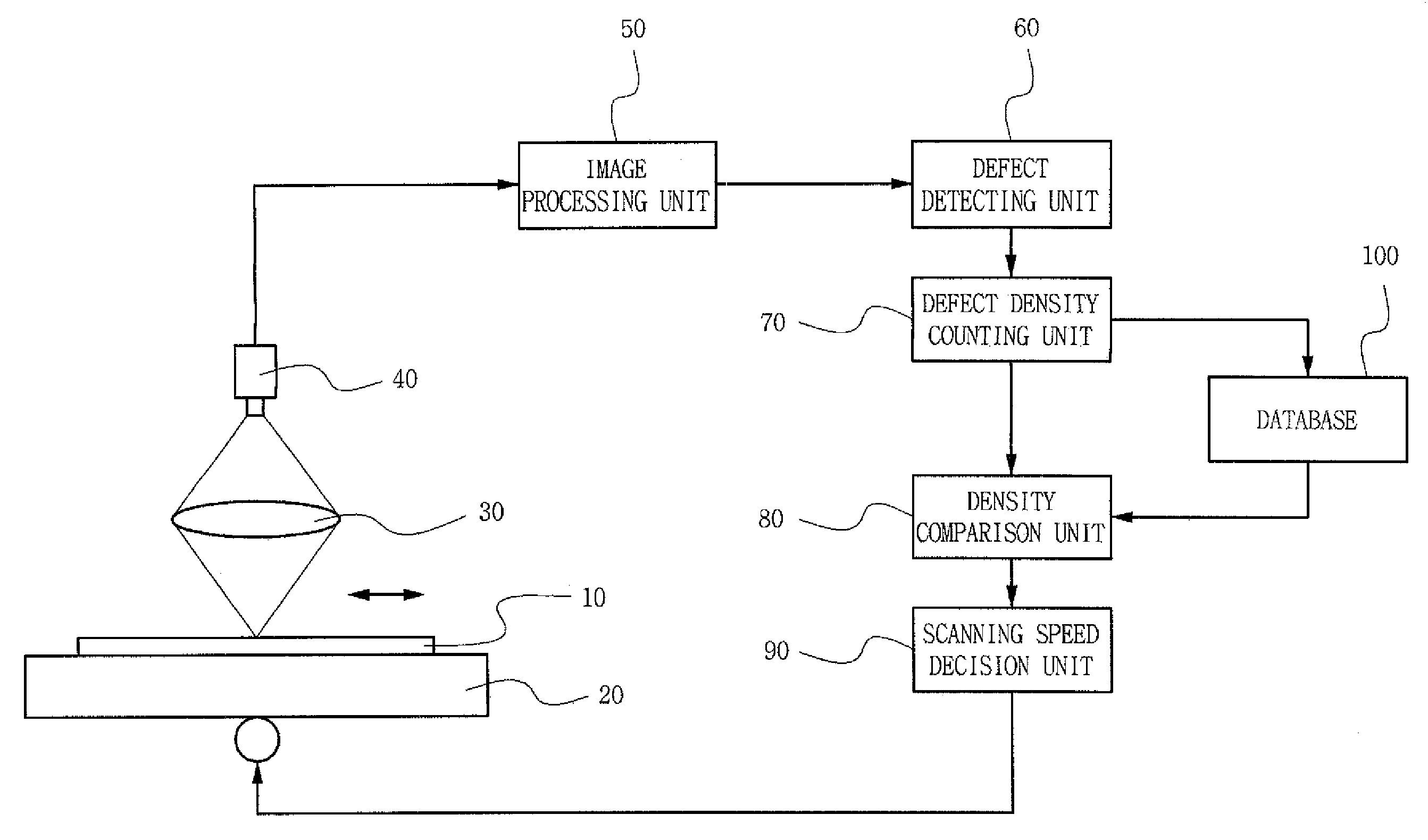
Apparatus and method for inspecting a surface of a wafer
PatentActiveUS7697130B2
Innovation
- A surface inspection apparatus and method that adjusts scanning speed based on defect density, using a stage with a moving wafer, an optical system for image projection, an image acquisition system, image processing, and a defect-detecting unit to compute and compare defect densities, thereby varying the scanning speed to enhance defect detection reliability and throughput.


Optical Mode Optimization for Wafer Inspection
PatentActiveUS20230367951A1
Innovation
- The method optimizes optical parameters through simulation rather than real wafer inspections, using a 3D model of the IC design layout to identify areas with potential defects, generating simulated optical images with candidate optical modes, and selecting the best mode for inspection, with retraining mechanisms to adapt to process changes.


Environmental Regulations for Semiconductor Manufacturing
The semiconductor manufacturing industry operates under increasingly stringent environmental regulations that directly impact continuous wafer inspection processes and their energy optimization strategies. These regulations encompass multiple jurisdictions and environmental aspects, creating a complex compliance landscape that manufacturers must navigate while pursuing energy efficiency improvements.
Air quality regulations represent a primary concern, with agencies like the EPA in the United States and similar bodies globally establishing strict limits on volatile organic compound emissions, particulate matter, and hazardous air pollutants. Continuous wafer inspection facilities must comply with National Emission Standards for Hazardous Air Pollutants, which often require advanced air filtration systems and emission monitoring equipment that consume significant energy. The challenge lies in balancing compliance requirements with energy optimization goals, as more sophisticated environmental controls typically demand higher power consumption.
Water usage and discharge regulations add another layer of complexity to energy efficiency optimization efforts. Semiconductor facilities face strict limits on water consumption and wastewater discharge quality under regulations such as the Clean Water Act. Continuous inspection processes often require ultrapure water systems and cooling mechanisms that are energy-intensive. Facilities must implement closed-loop water recycling systems and advanced treatment technologies to meet discharge standards, which can account for up to 30% of total facility energy consumption.
Chemical management regulations under frameworks like REACH in Europe and TSCA in the United States influence the selection of cleaning agents and process chemicals used in wafer inspection equipment. These regulations often favor environmentally safer alternatives that may require different processing conditions, potentially affecting energy consumption patterns. Compliance documentation and reporting requirements also necessitate additional monitoring systems and data collection infrastructure.
Greenhouse gas emission regulations, including carbon pricing mechanisms and mandatory reporting schemes, create direct financial incentives for energy efficiency improvements in continuous wafer inspection processes. Facilities subject to cap-and-trade programs or carbon taxes must carefully balance operational efficiency with environmental compliance costs. Many jurisdictions now require detailed energy audits and efficiency improvement plans as part of environmental permitting processes.
Waste management regulations governing electronic waste, chemical disposal, and hazardous materials handling impact equipment lifecycle decisions and maintenance practices in inspection facilities. Extended producer responsibility requirements and circular economy initiatives are driving manufacturers toward more sustainable equipment designs and operational practices that integrate environmental compliance with energy optimization objectives.
Cost-Benefit Analysis of Energy-Optimized Inspection Systems
The economic evaluation of energy-optimized wafer inspection systems reveals compelling financial advantages that extend beyond initial capital investments. Traditional continuous inspection systems typically consume 15-25% more energy than their optimized counterparts, translating to annual operational cost savings of $200,000-$500,000 for high-volume semiconductor facilities. These savings compound over the typical 7-10 year equipment lifecycle, generating substantial returns on investment.
Initial capital expenditure for energy-optimized inspection systems commands a premium of approximately 12-18% over conventional systems. However, this upfront investment is offset by reduced energy consumption, lower cooling requirements, and decreased maintenance costs. Advanced LED illumination systems, variable-speed motors, and intelligent power management contribute to 20-30% reduction in total energy consumption while maintaining inspection accuracy and throughput.
Operational benefits extend beyond direct energy savings to include reduced facility infrastructure requirements. Energy-efficient systems generate less heat, decreasing cleanroom cooling loads by 15-20% and reducing HVAC operational costs. Additionally, optimized systems demonstrate improved component longevity, with LED light sources lasting 3-5 times longer than traditional halogen alternatives, significantly reducing replacement costs and maintenance downtime.
The total cost of ownership analysis demonstrates payback periods of 18-24 months for most energy-optimized inspection implementations. Facilities processing over 10,000 wafers monthly achieve faster payback due to higher utilization rates. Environmental compliance benefits add further value, as reduced energy consumption helps meet corporate sustainability targets and may qualify for government incentives or carbon credit programs.
Risk mitigation represents another significant benefit, as energy-efficient systems typically exhibit lower failure rates and more predictable maintenance schedules. This reliability translates to reduced unplanned downtime costs, which can exceed $50,000 per hour in high-volume production environments. The combination of direct cost savings, operational improvements, and risk reduction creates a compelling business case for energy-optimized inspection system adoption across semiconductor manufacturing operations.
Unlock deeper insights with Patsnap Eureka Quick Research — get a full tech report to explore trends and direct your research. Try now!
Generate Your Research Report Instantly with AI Agent
Supercharge your innovation with Patsnap Eureka AI Agent Platform!