

Optimizing CVD Chamber Design for Dynamic Heating Uniformity
APR 8, 20269 MIN READ
Generate Your Research Report Instantly with AI Agent
PatSnap Eureka helps you evaluate technical feasibility & market potential.
CVD Chamber Heating Uniformity Background and Objectives
Chemical Vapor Deposition (CVD) has emerged as a cornerstone technology in semiconductor manufacturing, thin film production, and advanced materials synthesis since its commercial introduction in the 1960s. The process involves the chemical reaction of gaseous precursors on heated substrates to form solid thin films with precise thickness control and exceptional uniformity. As semiconductor devices have evolved toward smaller feature sizes and larger wafer diameters, the demands for heating uniformity within CVD chambers have intensified dramatically.
The evolution of CVD technology has been driven by the semiconductor industry's relentless pursuit of Moore's Law, requiring increasingly sophisticated process control mechanisms. Early CVD systems utilized simple resistance heating elements, but modern applications demand complex multi-zone heating systems capable of maintaining temperature variations within ±1°C across 300mm wafers. This precision requirement has become even more critical with the advent of 3D NAND structures and advanced logic devices operating at sub-7nm technology nodes.
Current market drivers include the exponential growth in memory device production, the proliferation of Internet of Things applications, and the emergence of artificial intelligence chips requiring specialized materials. These applications demand CVD processes capable of depositing ultra-thin films with atomic-level precision, making heating uniformity a fundamental enabler rather than merely a process optimization parameter.
The primary objective of optimizing CVD chamber design for dynamic heating uniformity centers on achieving real-time temperature control across the entire substrate surface during deposition processes. This involves developing advanced heating element configurations, implementing sophisticated thermal modeling algorithms, and integrating feedback control systems that can respond to process variations within milliseconds.
Secondary objectives include minimizing thermal stress-induced defects, reducing process cycle times through faster temperature ramping capabilities, and extending equipment lifetime by eliminating hot spots that cause premature component failure. The ultimate goal is establishing a robust platform technology that can adapt to diverse material systems while maintaining the stringent uniformity requirements demanded by next-generation semiconductor manufacturing processes.
These objectives align with industry roadmaps projecting continued scaling challenges and the need for innovative process technologies that can support emerging applications in quantum computing, neuromorphic devices, and advanced packaging solutions requiring unprecedented material property control.
Market Demand for Advanced CVD Equipment
The semiconductor industry's relentless pursuit of smaller node technologies and enhanced device performance has created substantial market demand for advanced CVD equipment with superior heating uniformity capabilities. As manufacturers transition to sub-7nm processes and explore next-generation materials like gallium nitride and silicon carbide, the requirements for precise temperature control during deposition have become increasingly stringent.
Market drivers stem primarily from the expanding applications of semiconductor devices across automotive electronics, 5G infrastructure, artificial intelligence processors, and Internet of Things devices. These applications demand higher performance chips with improved electrical characteristics, which directly correlates with the uniformity of thin film deposition processes. The automotive sector's shift toward electric vehicles and autonomous driving systems has particularly intensified demand for power semiconductors requiring exceptional material quality.
The compound semiconductor market represents a significant growth segment driving CVD equipment demand. Wide bandgap materials used in power electronics and RF applications require precise thermal management during epitaxial growth processes. Traditional CVD systems often struggle to maintain uniform heating across large wafer surfaces, creating opportunities for advanced chamber designs with dynamic heating capabilities.
Memory manufacturers face increasing pressure to achieve higher storage densities while maintaining yield rates. Three-dimensional NAND flash and emerging memory technologies like MRAM require multiple deposition steps with exacting temperature specifications. Non-uniform heating can result in thickness variations that compromise device performance and reduce manufacturing yields, making advanced CVD systems essential for competitive production.
The rise of heterogeneous integration and advanced packaging technologies has created new market segments requiring specialized CVD processes. These applications often involve depositing materials on substrates with varying thermal properties, necessitating dynamic heating control to compensate for thermal gradients and ensure uniform film characteristics across the entire substrate surface.
Geographically, the Asia-Pacific region dominates CVD equipment demand, driven by major foundries and memory manufacturers expanding production capacity. However, growing semiconductor manufacturing initiatives in North America and Europe are creating additional market opportunities for advanced CVD systems with enhanced heating uniformity features.
Equipment manufacturers are responding to these market demands by developing next-generation CVD systems incorporating advanced heating technologies, real-time temperature monitoring, and adaptive control algorithms to achieve unprecedented levels of thermal uniformity across various substrate sizes and materials.
Current CVD Chamber Design Challenges and Limitations
Current CVD chamber designs face significant thermal management challenges that directly impact process uniformity and product quality. Traditional heating systems often rely on resistive heating elements or lamp-based configurations that create inherent temperature gradients across the substrate surface. These gradients become particularly problematic as wafer sizes increase to 300mm and beyond, where even minor temperature variations can result in substantial film thickness non-uniformities and property variations across the substrate.
The complexity of achieving dynamic heating uniformity is compounded by the multi-zone heating requirements in modern CVD processes. Conventional chamber designs struggle to provide independent temperature control across different substrate regions while maintaining rapid thermal response capabilities. This limitation becomes critical during temperature ramping sequences and multi-step processes where precise temporal and spatial temperature control is essential for optimal film deposition.
Gas flow dynamics present another fundamental challenge in current CVD chamber architectures. The interaction between heating elements and gas distribution systems often creates unwanted thermal boundary layers and flow disturbances that compromise both temperature uniformity and precursor delivery consistency. Traditional showerhead designs, while effective for gas distribution, can create shadowing effects that interfere with radiant heating patterns, leading to localized temperature variations.
Thermal mass distribution represents a persistent design constraint in existing CVD chambers. Heavy heating elements and support structures create thermal inertia that limits the system's ability to respond quickly to temperature setpoint changes. This sluggish thermal response not only reduces process flexibility but also makes it difficult to implement advanced temperature control algorithms that could compensate for spatial non-uniformities through dynamic heating adjustments.
Chamber geometry limitations further restrict optimization possibilities in current designs. The need to accommodate multiple heating zones, gas injection systems, and substrate handling mechanisms within confined spaces often results in compromised thermal designs. Traditional cylindrical or rectangular chamber geometries may not provide optimal heat distribution patterns, particularly when considering the complex interplay between radiant, conductive, and convective heat transfer mechanisms.
Sensor placement and feedback control systems in existing CVD chambers often lack the spatial resolution necessary for true dynamic heating uniformity. Limited temperature monitoring points and slow sensor response times prevent real-time compensation for thermal non-uniformities. Additionally, the harsh chemical environment within CVD chambers restricts sensor placement options and can degrade measurement accuracy over time, further limiting the effectiveness of closed-loop temperature control systems.
Existing Dynamic Heating Solutions
01 Multi-zone heating element design for uniform temperature distribution
CVD chambers can achieve heating uniformity through the implementation of multi-zone heating elements with independent temperature control. This approach allows for precise adjustment of heat distribution across different regions of the chamber, compensating for heat loss variations and ensuring consistent substrate temperature. The heating elements are strategically positioned and individually controlled to create uniform thermal profiles across the processing area.- Multi-zone heating element design for temperature control: CVD chambers can achieve heating uniformity through the implementation of multi-zone heating elements that allow independent temperature control in different regions. This approach enables precise adjustment of heat distribution across the chamber, compensating for thermal gradients and ensuring uniform substrate temperature. The heating zones can be concentrically arranged or segmented to address specific hot or cold spots within the processing area.
- Optimized heater geometry and placement: The geometric configuration and positioning of heating elements significantly impacts temperature uniformity in CVD chambers. Strategic placement of heaters, including radial positioning and distance from substrates, can minimize temperature variations. Design considerations include heater shape, surface area distribution, and thermal coupling with chamber components to achieve balanced heat transfer throughout the processing volume.
- Thermal shielding and insulation structures: Implementing thermal shields and insulation components helps maintain heating uniformity by controlling heat loss and radiation patterns within CVD chambers. These structures can include reflective barriers, heat distribution plates, and insulating materials strategically positioned to redirect thermal energy and reduce edge effects. Such designs prevent excessive heat dissipation in certain areas while promoting even temperature distribution across the substrate.
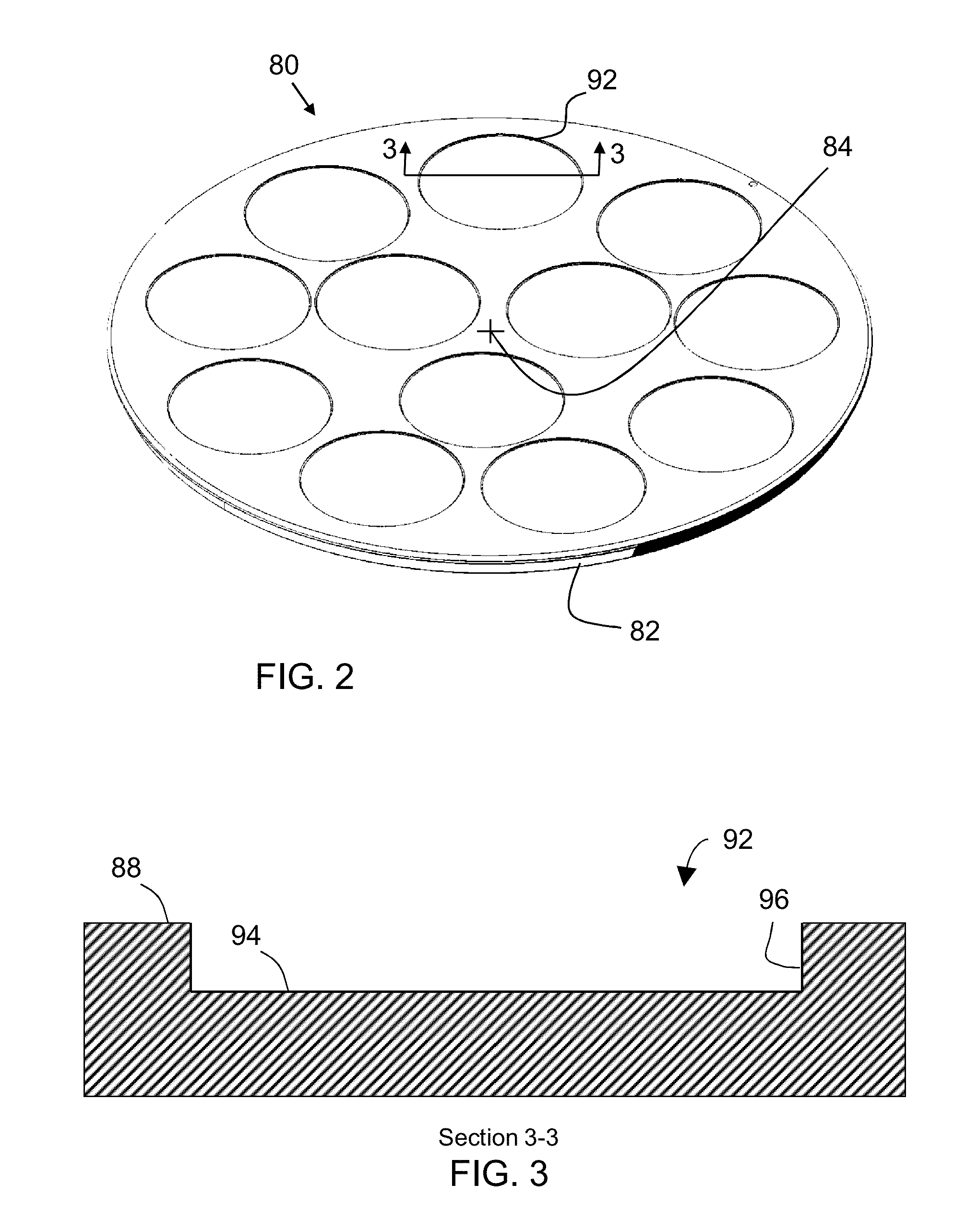
- Substrate support and susceptor design: The design of substrate supports and susceptors plays a critical role in achieving uniform heating in CVD processes. Features such as material selection, thickness variation, thermal mass distribution, and contact geometry with heating elements influence heat transfer to the substrate. Advanced susceptor designs may incorporate variable thickness profiles or embedded heating elements to compensate for inherent temperature non-uniformities.
- Temperature monitoring and feedback control systems: Active temperature control systems utilizing multiple sensors and feedback mechanisms enable real-time adjustment of heating parameters to maintain uniformity. These systems monitor temperature at various chamber locations and dynamically adjust power delivery to different heating zones. Advanced control algorithms can predict and compensate for thermal variations, ensuring consistent processing conditions throughout the deposition cycle.
02 Optimized heater geometry and configuration
Heating uniformity can be improved through specialized heater geometries and configurations that account for edge effects and thermal gradients. This includes the use of segmented heaters, spiral patterns, or concentric ring designs that provide differential heating power to different zones. The geometric optimization ensures that heat flux is appropriately distributed to counteract natural temperature variations within the chamber.Expand Specific Solutions03 Thermal shielding and insulation structures
Implementation of thermal shielding and insulation structures helps maintain heating uniformity by minimizing heat loss and preventing unwanted thermal radiation. These structures include reflective shields, insulation layers, and thermal barriers strategically placed within the chamber to direct heat flow and reduce temperature gradients. The design ensures that heat is retained in the processing zone and distributed evenly across the substrate.Expand Specific Solutions04 Temperature monitoring and feedback control systems
Advanced temperature monitoring systems with multiple sensors and feedback control mechanisms enable real-time adjustment of heating parameters to maintain uniformity. These systems continuously measure temperature at various locations within the chamber and automatically adjust power delivery to individual heating zones. The closed-loop control ensures consistent thermal conditions throughout the deposition process.Expand Specific Solutions05 Substrate support and rotation mechanisms
Heating uniformity can be enhanced through specialized substrate support structures and rotation mechanisms that promote even heat distribution. These include susceptors with optimized thermal properties, rotating substrate holders, and lift pin arrangements that ensure consistent thermal contact. The mechanical design facilitates uniform heat transfer from the heating elements to the substrate surface, eliminating hot spots and cold zones.Expand Specific Solutions
Key Players in CVD Equipment Industry
The CVD chamber design optimization market represents a mature yet rapidly evolving sector within the broader semiconductor equipment industry, currently valued at approximately $15-20 billion globally. The industry is in a consolidation phase, dominated by established players like Applied Materials, AIXTRON SE, and Veeco Instruments, who possess decades of expertise in thermal management and deposition technologies. Technology maturity varies significantly across market segments, with companies like Eugene Technology and Advanced Micro Fabrication Equipment driving innovation in next-generation heating uniformity solutions, while traditional leaders focus on scaling existing technologies. Asian manufacturers including Beijing NAURA Microelectronics and SMIC-Beijing are rapidly advancing their capabilities, creating competitive pressure on established Western firms. The market shows strong growth potential driven by increasing demand for advanced semiconductors, though technical barriers remain high, requiring substantial R&D investments in thermal modeling, chamber materials, and process control systems to achieve optimal heating uniformity across diverse substrate sizes and materials.
Beijing NAURA Microelectronics Equipment Co., Ltd.
Technical Solution: NAURA has developed indigenous CVD chamber technologies focusing on multi-zone heating systems with advanced thermal control capabilities. Their approach incorporates distributed heating elements with independent zone control, enabling precise temperature management across large substrate areas. The company's chambers feature sophisticated susceptor designs with embedded heating elements and real-time temperature monitoring systems. NAURA's thermal management solutions include computational modeling for heat distribution optimization and advanced control algorithms for dynamic heating adjustment. Their systems utilize multiple temperature sensors and feedback control mechanisms to maintain uniform heating profiles during various CVD processes. The company has implemented proprietary heating control software that enables real-time adjustment of heating parameters based on process conditions and substrate characteristics.
Strengths: Cost-effective solutions with strong local market presence and customizable heating control systems for specific applications. Weaknesses: Limited global market penetration and relatively newer technology compared to established international competitors.
Applied Materials, Inc.
Technical Solution: Applied Materials has developed advanced CVD chamber designs featuring multi-zone heating systems with independent temperature control capabilities. Their Centura platform incorporates sophisticated thermal management solutions including radiant heating elements with real-time temperature monitoring and feedback control systems. The company's approach utilizes computational fluid dynamics modeling to optimize gas flow patterns and heat distribution, ensuring uniform temperature profiles across wafer surfaces. Their chambers feature advanced susceptor designs with embedded heating elements and pyrometric temperature sensing for precise thermal control. The integration of AI-driven process control algorithms enables dynamic adjustment of heating parameters based on real-time process conditions, achieving temperature uniformity within ±2°C across 300mm wafers during deposition processes.
Strengths: Market-leading position with comprehensive thermal control solutions and proven scalability for high-volume manufacturing. Weaknesses: High capital costs and complex system integration requirements may limit adoption for smaller fabs.
Core Innovations in Thermal Management Systems
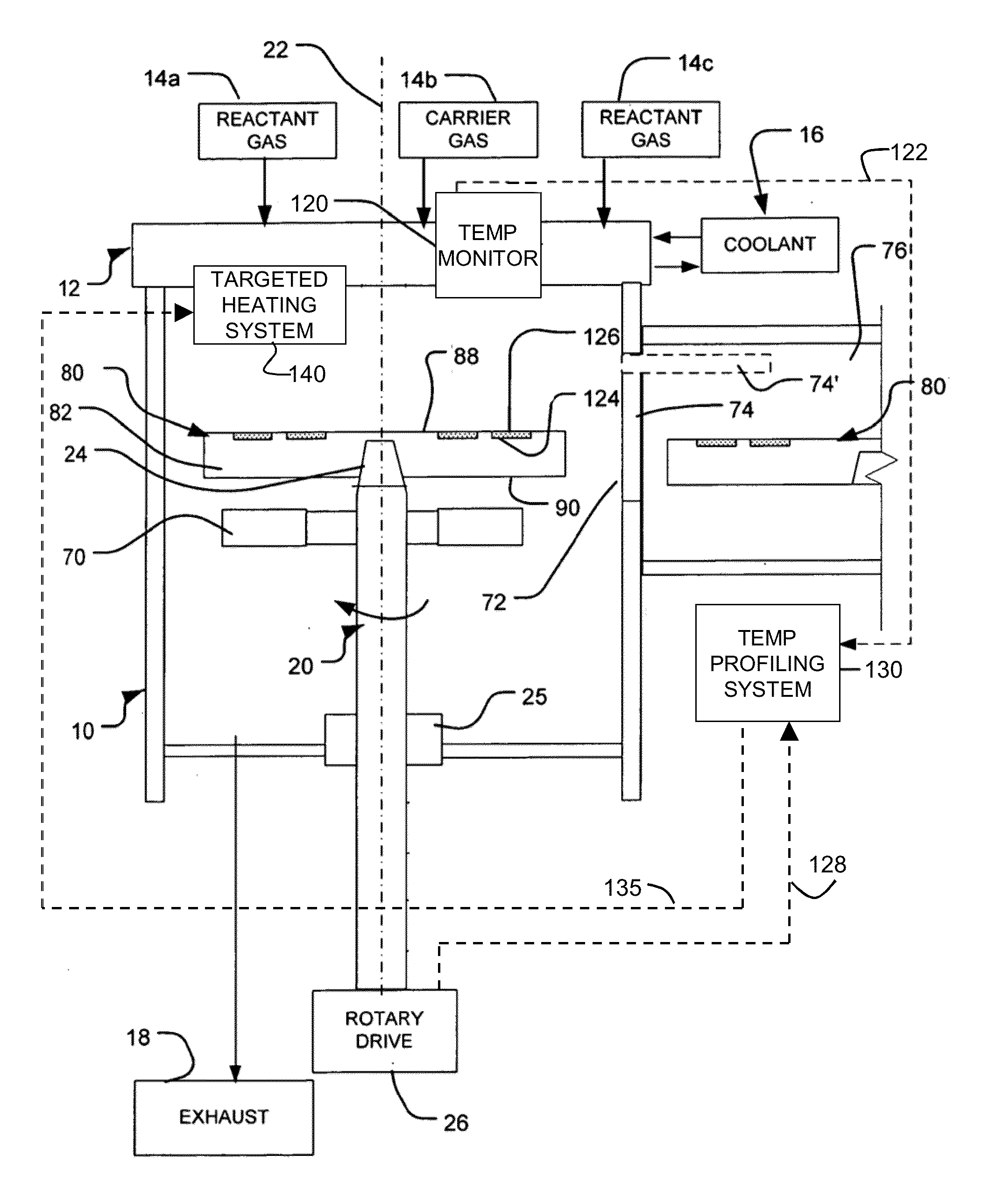
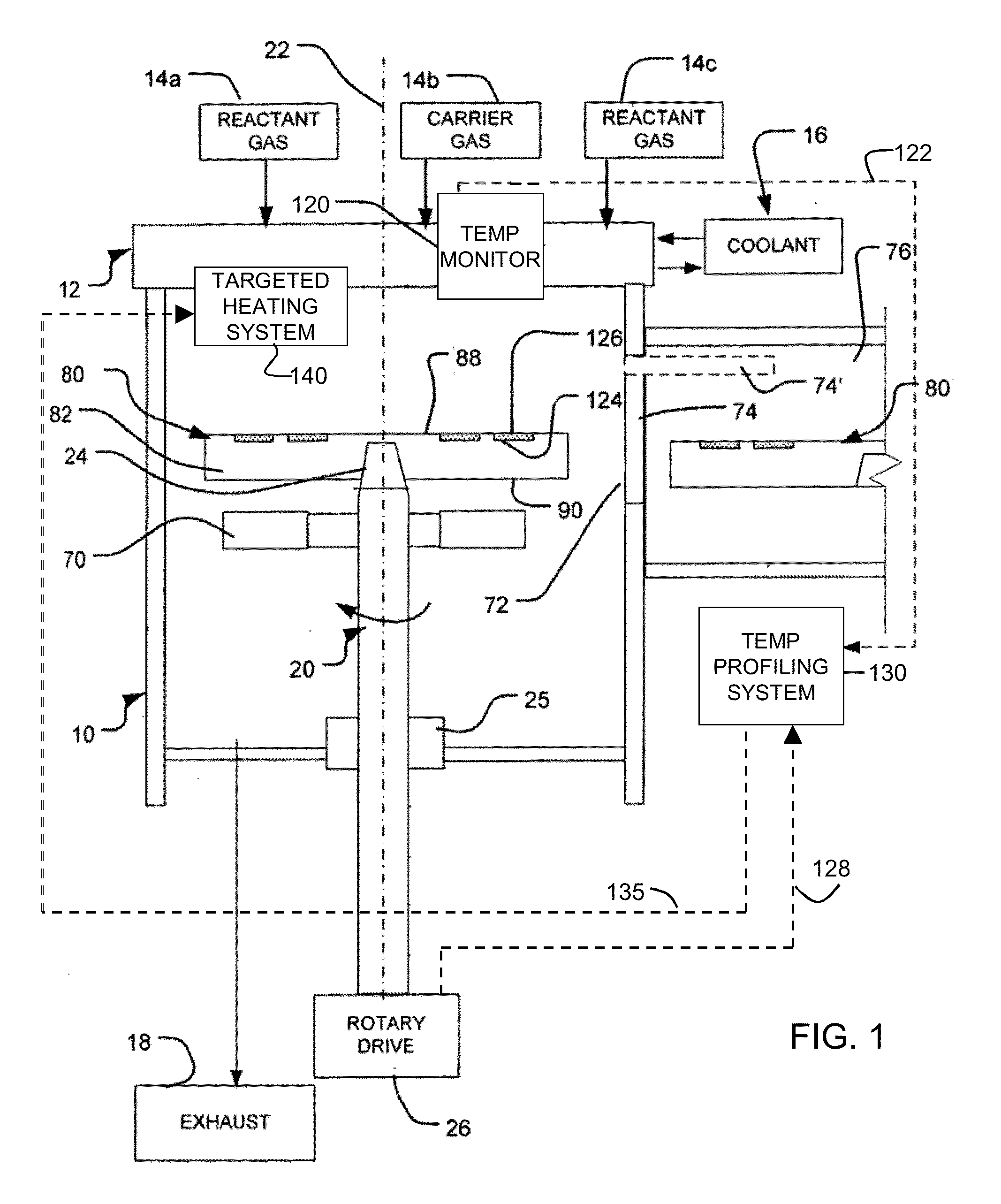
Targeted temperature compensation in chemical vapor deposition systems
PatentInactiveUS20130167769A1
Innovation
- A CVD system with a localized temperature monitoring and targeted heating system that dynamically corrects thermal non-uniformities by generating temperature profiles and applying selective heat to cold spots using an ultraviolet pulsed laser, ensuring uniform thermal distribution during the CVD process.

Process-specific wafer carrier correction to improve thermal uniformity in chemical vapor deposition systems and processes
PatentWO2017031106A1
Innovation
- A system that customizes wafer carriers using thermal modeling and simulation to optimize pocket floor design, applying structural corrections based on computational models to enhance thermal uniformity without requiring measurements of fabricated devices, utilizing a computing platform with engines for thermal model generation, simulation, and pocket floor correction.


Process Control and Monitoring Standards
Process control and monitoring standards for CVD chamber design optimization represent a critical framework that ensures consistent dynamic heating uniformity across semiconductor manufacturing operations. These standards encompass real-time temperature monitoring protocols, automated feedback control systems, and comprehensive data acquisition methodologies that collectively maintain thermal stability within specified tolerances.
Temperature monitoring standards require implementation of multi-point sensing arrays strategically positioned throughout the chamber volume. Industry-standard thermocouple configurations typically include radial and axial measurement points, with sampling frequencies exceeding 10 Hz to capture rapid thermal transients. Advanced monitoring systems integrate infrared pyrometry and resistance temperature detectors to provide redundant temperature validation across different measurement principles.
Control loop standards mandate closed-loop feedback systems with proportional-integral-derivative algorithms specifically tuned for CVD thermal dynamics. Response time requirements typically specify correction actions within 2-3 seconds of detecting temperature deviations exceeding ±2°C from setpoint values. These control standards also define heating zone independence criteria, ensuring individual zone adjustments do not adversely affect neighboring regions.
Data logging and traceability standards require comprehensive recording of all thermal parameters, including heating element power consumption, gas flow rates, and chamber pressure correlations. Statistical process control methodologies must demonstrate temperature uniformity within ±1% across the substrate surface, with capability indices exceeding 1.33 for critical process parameters.
Calibration standards establish regular verification protocols for all sensing and control equipment, typically requiring monthly calibration cycles for production environments. These standards also define acceptable drift tolerances and corrective action procedures when monitoring systems exceed specified accuracy limits.
Safety interlock standards integrate emergency shutdown procedures triggered by temperature excursions beyond safe operating limits. These protective measures include automatic power reduction sequences and inert gas purging protocols to prevent equipment damage and ensure operator safety during abnormal thermal conditions.
Energy Efficiency and Environmental Impact
Energy efficiency represents a critical performance metric for CVD chamber operations, directly impacting manufacturing costs and operational sustainability. Traditional heating systems in CVD chambers often exhibit significant energy losses through radiation, conduction, and convection pathways. Dynamic heating uniformity optimization addresses these inefficiencies by implementing intelligent thermal management strategies that reduce overall power consumption while maintaining precise temperature control across the substrate surface.
Advanced chamber designs incorporate multi-zone heating elements with independent control capabilities, enabling localized energy delivery based on real-time thermal mapping. This approach eliminates energy waste associated with overheating specific regions to compensate for cold spots elsewhere. Predictive heating algorithms further enhance efficiency by anticipating thermal requirements and adjusting power distribution proactively, reducing energy spikes and maintaining steady-state conditions with minimal power fluctuations.
The environmental impact of CVD processes extends beyond energy consumption to encompass waste heat management and resource utilization. Optimized chamber designs integrate heat recovery systems that capture and redirect thermal energy for preheating incoming gases or maintaining auxiliary systems. This closed-loop approach significantly reduces the overall environmental footprint while improving process economics.
Emission reduction strategies focus on minimizing volatile organic compounds and particulate matter release through enhanced chamber sealing and exhaust management systems. Dynamic heating uniformity contributes to reduced process variability, leading to fewer defective products and decreased material waste. Improved temperature control also enables lower processing temperatures for certain applications, reducing energy requirements and extending equipment lifespan.
Lifecycle assessment considerations reveal that energy-efficient CVD chambers demonstrate substantially lower carbon footprints compared to conventional systems. The integration of renewable energy sources becomes more feasible with optimized power consumption profiles, supporting corporate sustainability initiatives. Additionally, reduced thermal stress on chamber components through uniform heating extends equipment durability, minimizing replacement frequency and associated manufacturing environmental impacts.
Regulatory compliance increasingly demands environmental performance documentation, making energy efficiency optimization a strategic necessity rather than merely an operational improvement. Advanced monitoring systems provide real-time energy consumption data and environmental impact metrics, enabling continuous optimization and regulatory reporting capabilities.
Unlock deeper insights with PatSnap Eureka Quick Research — get a full tech report to explore trends and direct your research. Try now!
Generate Your Research Report Instantly with AI Agent
Supercharge your innovation with PatSnap Eureka AI Agent Platform!