

Optimizing Deposition Chamber Geometry For PVD
APR 8, 20269 MIN READ
Generate Your Research Report Instantly with AI Agent
PatSnap Eureka helps you evaluate technical feasibility & market potential.
PVD Chamber Geometry Background and Objectives
Physical Vapor Deposition (PVD) technology has evolved significantly since its inception in the 1930s, transitioning from simple evaporation techniques to sophisticated sputtering and ion beam deposition systems. The fundamental principle involves the physical transfer of material from a target source to a substrate through vapor phase transport, enabling precise thin film formation with exceptional control over thickness, composition, and microstructure.
The evolution of PVD chamber design has been driven by increasingly demanding applications across semiconductor manufacturing, optical coatings, decorative finishes, and advanced materials engineering. Early chamber configurations were relatively simple, focusing primarily on basic material transport. However, as industry requirements intensified, the need for optimized chamber geometries became paramount to achieve uniform deposition, minimize contamination, and enhance process efficiency.
Modern PVD applications require unprecedented levels of precision and uniformity. Semiconductor devices demand atomic-level thickness control across large wafer surfaces, while optical coatings necessitate exceptional uniformity to maintain consistent refractive indices. These stringent requirements have positioned chamber geometry optimization as a critical technological frontier, directly impacting yield, performance, and manufacturing economics.
The primary objective of optimizing PVD chamber geometry centers on achieving superior deposition uniformity across substrate surfaces while maintaining high deposition rates and material utilization efficiency. This involves strategic positioning of targets, substrates, and auxiliary components to create optimal flux distributions and minimize shadowing effects that can compromise film quality.
Secondary objectives include minimizing particle contamination through improved gas flow dynamics, reducing cross-contamination between different materials, and enhancing process repeatability. Advanced chamber designs also target improved target utilization efficiency, extending operational lifetimes and reducing material waste, which directly impacts manufacturing costs.
Temperature management represents another crucial objective, as optimized geometries must facilitate effective thermal control to prevent substrate damage while maintaining optimal deposition conditions. This requires careful consideration of heating element placement, cooling system integration, and thermal isolation strategies.
The ultimate goal encompasses developing chamber architectures that can accommodate diverse substrate sizes and geometries while maintaining consistent performance parameters. This flexibility is essential for modern manufacturing environments where product portfolios frequently evolve, requiring adaptable deposition systems that can efficiently handle varying production requirements without compromising quality standards.
Market Demand for Advanced PVD Coating Solutions
The global market for advanced PVD coating solutions is experiencing robust growth driven by increasing demand across multiple high-technology sectors. Semiconductor manufacturing represents one of the most significant demand drivers, where precise thin-film deposition is critical for producing advanced microprocessors, memory devices, and power electronics. The continuous miniaturization of electronic components and the transition to next-generation technologies such as 5G, artificial intelligence chips, and quantum computing devices are creating unprecedented requirements for coating uniformity and precision.
Automotive industry transformation toward electric vehicles and autonomous driving systems has emerged as another major growth catalyst. Advanced PVD coatings are essential for manufacturing high-performance batteries, electric motor components, and sophisticated sensor systems. The industry's shift toward lightweight materials and enhanced durability requirements further amplifies the need for optimized deposition processes that can deliver superior coating properties with minimal material waste.
Aerospace and defense applications continue to drive demand for specialized PVD coating solutions, particularly for turbine engine components, satellite systems, and advanced weaponry. These applications require coatings with exceptional thermal resistance, corrosion protection, and mechanical durability, necessitating precise control over deposition parameters that can only be achieved through optimized chamber geometries.
The renewable energy sector, particularly solar photovoltaic and wind power industries, represents a rapidly expanding market segment. Solar panel manufacturing requires uniform thin-film deposition across large substrate areas, while wind turbine components benefit from protective coatings that extend operational lifespans in harsh environmental conditions.
Medical device manufacturing has become increasingly dependent on advanced PVD coatings for biocompatible implants, surgical instruments, and diagnostic equipment. The growing aging population and increasing healthcare expenditure globally are driving sustained demand for high-quality medical devices with superior surface properties.
Market dynamics indicate a clear preference for PVD systems that can deliver enhanced throughput, improved coating uniformity, and reduced operational costs. Equipment manufacturers are responding by developing innovative chamber designs that optimize plasma distribution, substrate heating, and target utilization efficiency. The integration of advanced process monitoring and control systems is becoming a standard requirement for meeting stringent quality specifications across all application sectors.
Current PVD Chamber Design Challenges and Limitations
Physical Vapor Deposition (PVD) chamber design faces significant challenges in achieving uniform film thickness across large substrates while maintaining high deposition rates. Traditional chamber geometries often result in non-uniform coating distribution, with thickness variations exceeding 5-10% across wafer surfaces, particularly problematic for advanced semiconductor applications requiring sub-nanometer precision.
Thermal management represents a critical limitation in current PVD systems. Conventional chamber designs struggle to maintain consistent temperature profiles during high-power sputtering processes, leading to substrate warping and stress-induced defects. The asymmetric heat distribution caused by standard magnetron configurations creates hot spots that compromise film quality and reduce process repeatability.
Target utilization efficiency remains suboptimal in existing chamber architectures. Standard planar magnetron designs typically achieve only 20-30% target material utilization before requiring replacement, resulting in significant material waste and increased operational costs. The magnetic field configuration in conventional chambers creates preferential erosion patterns that limit target lifetime and affect deposition uniformity over time.
Contamination control poses ongoing challenges due to inadequate chamber geometry optimization. Current designs often feature dead zones where reactive gases accumulate, leading to particle generation and film contamination. The positioning of pumping ports and gas injection systems in traditional chambers creates turbulent flow patterns that compromise process cleanliness and yield.
Scalability limitations become apparent when adapting existing chamber designs for larger substrate sizes or higher throughput requirements. Conventional PVD chambers designed for 200mm wafers face significant engineering challenges when scaled to 300mm or larger formats, with uniformity and process control becoming increasingly difficult to maintain.
Process flexibility constraints in current chamber designs limit the ability to accommodate diverse material systems and deposition requirements. Fixed target-to-substrate distances and rigid magnetic field configurations restrict the optimization potential for different applications, forcing compromises between deposition rate, uniformity, and film properties.
Gas flow dynamics in existing chambers often exhibit poor distribution characteristics, with inadequate mixing and residence time control. This limitation affects reactive sputtering processes where precise stoichiometry control is essential, leading to compositional variations across the substrate surface and batch-to-batch inconsistencies.
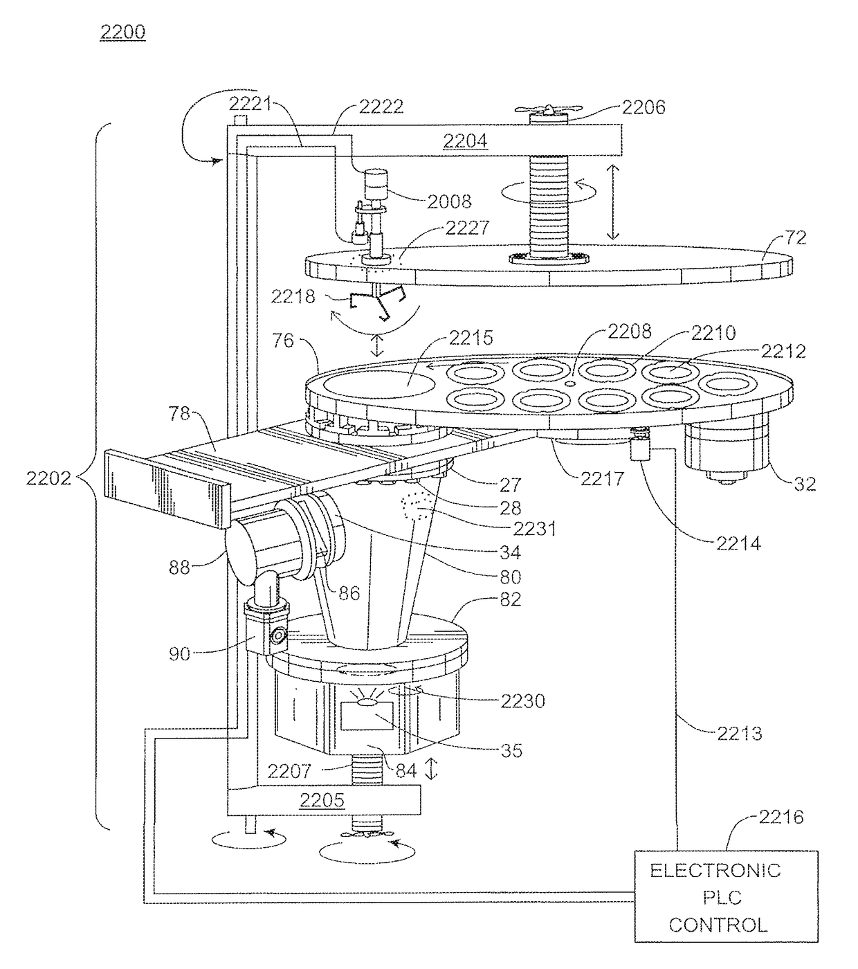
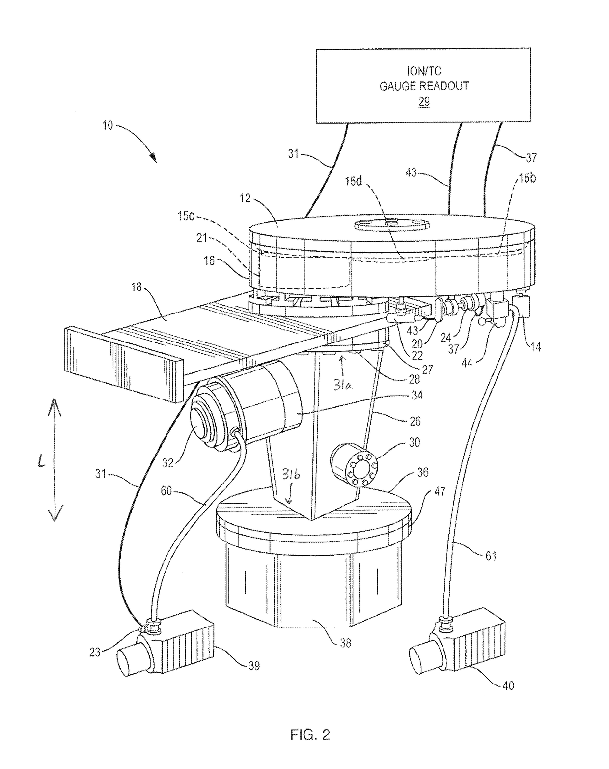
Existing Chamber Geometry Optimization Solutions
01 Chamber configuration with optimized substrate positioning
PVD deposition chambers can be designed with specific geometric configurations to optimize substrate positioning relative to the target material. The chamber geometry includes arrangements for substrate holders, rotation mechanisms, and distance control between substrate and target to ensure uniform coating thickness. These configurations may incorporate tilting mechanisms and multi-axis positioning systems to achieve desired deposition angles and coverage patterns.- Chamber configuration with optimized substrate positioning: PVD deposition chambers can be designed with specific geometric configurations to optimize substrate positioning relative to the target material. The chamber geometry includes arrangements for substrate holders, rotation mechanisms, and distance control between substrate and target to ensure uniform coating thickness. These configurations may incorporate tilting mechanisms and multi-axis positioning systems to achieve better deposition uniformity across the substrate surface.
- Target and source arrangement geometry: The geometric arrangement of targets and deposition sources within the chamber significantly affects deposition characteristics. This includes the positioning of multiple targets, their angular orientation, and spacing relative to the substrate. Various configurations such as planar, cylindrical, or conical target arrangements can be employed to control the flux distribution and deposition rate across the substrate area.
- Chamber wall and shield design: The internal geometry of chamber walls and protective shields plays a crucial role in controlling particle trajectories and preventing contamination. Shield designs include specific angles, curvatures, and aperture configurations that direct material flux while minimizing unwanted deposition on chamber components. The geometric features help maintain process stability and reduce maintenance requirements.
- Gas flow and pressure distribution geometry: Chamber geometry incorporates specific features for controlling gas flow patterns and pressure distribution during deposition. This includes the design of gas inlet and outlet positions, baffle arrangements, and pumping port configurations. The geometric design ensures uniform gas distribution, proper evacuation, and optimal working pressure throughout the deposition zone to achieve consistent film properties.
- Heating and cooling system integration: The chamber geometry includes integrated heating and cooling elements positioned to maintain optimal temperature control during deposition. This encompasses the geometric design of heating elements, cooling channels, and thermal shields arranged to provide uniform temperature distribution across the substrate. The spatial arrangement of these thermal management components is critical for process control and film quality.
02 Target and magnetron arrangement geometry
The geometric arrangement of targets and magnetron assemblies within the deposition chamber significantly affects deposition uniformity and efficiency. Chamber designs incorporate specific positioning of planar or cylindrical magnetrons, target-to-substrate spacing, and angular orientations. The geometry may include multiple target configurations, rotatable magnetrons, and optimized magnetic field distributions to enhance plasma confinement and material utilization.Expand Specific Solutions03 Chamber wall and shield geometry
The internal geometry of chamber walls and protective shields plays a crucial role in controlling deposition patterns and preventing contamination. Design features include shaped chamber walls, removable shields with specific contours, and geometric arrangements that minimize particle generation and optimize gas flow. The shield geometry helps direct material flux and protects chamber components from unwanted coating buildup.Expand Specific Solutions04 Gas distribution and flow geometry
Chamber geometry incorporates specific gas inlet and outlet configurations to achieve optimal gas distribution and pressure uniformity. Design elements include strategically positioned gas injection ports, baffle arrangements, and exhaust geometries that promote laminar flow patterns. The geometric design of gas distribution systems ensures uniform plasma generation and efficient removal of reaction byproducts throughout the deposition zone.Expand Specific Solutions05 Multi-chamber and cluster tool geometry
Advanced PVD systems utilize multi-chamber geometric configurations where multiple deposition chambers are arranged in cluster formations. The geometry includes transfer chambers, load-lock arrangements, and interconnecting passages that enable sequential processing without breaking vacuum. These geometric layouts optimize substrate handling, reduce contamination, and enable multi-layer deposition processes with different materials in separate chambers.Expand Specific Solutions
Key Players in PVD Equipment Manufacturing Industry
The PVD deposition chamber geometry optimization market represents a mature segment within the broader semiconductor equipment industry, currently valued at approximately $65 billion globally. The industry is in a consolidation phase, dominated by established equipment manufacturers who control critical fabrication technologies. Technology maturity varies significantly across market participants, with Applied Materials, Tokyo Electron, and Novellus Systems leading in advanced PVD system development and chamber design optimization. Taiwan Semiconductor Manufacturing and United Microelectronics represent major foundry customers driving demand for enhanced deposition uniformity and throughput. Chinese players including Beijing NAURA, Shanghai Bitong Semiconductor, and SMIC are rapidly advancing their capabilities, while research institutions like Zhejiang University contribute fundamental innovations. The competitive landscape shows clear technological stratification, where established leaders maintain advantages in precision engineering and process control, while emerging players focus on cost-effective solutions and specialized applications.
Applied Materials, Inc.
Technical Solution: Applied Materials has developed advanced chamber geometry optimization technologies for PVD systems, including the Endura platform with multi-chamber architecture that enables precise control of deposition uniformity across wafer surfaces. Their chamber designs incorporate sophisticated gas flow dynamics modeling and target-to-substrate distance optimization to achieve better than 2% thickness uniformity on 300mm wafers. The company utilizes computational fluid dynamics (CFD) simulations combined with plasma modeling to optimize chamber geometries for specific applications, including advanced node semiconductor manufacturing and emerging materials deposition. Their chambers feature adjustable magnetron configurations and optimized gas injection systems that can be tailored for different target materials and deposition requirements.
Strengths: Market-leading uniformity control, extensive R&D capabilities, comprehensive process optimization tools. Weaknesses: High equipment costs, complex system integration requirements.
Beijing NAURA Microelectronics Equipment Co., Ltd.
Technical Solution: NAURA has developed cost-effective PVD chamber geometries optimized for high-volume manufacturing with focus on target utilization efficiency and process stability. Their chamber designs incorporate advanced magnetron sputtering configurations with optimized magnetic field distributions to enhance plasma density uniformity. The company's systems feature innovative gas injection schemes and chamber wall conditioning protocols to minimize cross-contamination between different materials. NAURA's chambers utilize proprietary substrate rotation mechanisms and heating systems to achieve consistent film properties across large substrate areas. Their designs emphasize ease of maintenance and reduced operational costs while maintaining competitive deposition uniformity and throughput performance for mainstream semiconductor applications.
Strengths: Cost-effective solutions, good target utilization efficiency, simplified maintenance procedures. Weaknesses: Limited advanced node capabilities, smaller global market presence compared to established players.
Core Innovations in PVD Chamber Design Patents
Physical vapor deposition in-chamber electro-magnet
PatentWO2019217046A1
Innovation
- A PVD chamber equipped with a coil portion of an electromagnet that can be energized with direct current (DC) power to modify plasma distribution and density, allowing for dynamic adjustment of the magnetic field to enhance film uniformity without requiring redesign of chamber components.


Physical vapor deposition apparatus having a tapered chamber
PatentActiveUS9920418B1
Innovation
- A PVD apparatus with a Tapered Load-Locked Chamber (TLC) configuration, comprising a load-lock deposition chamber, a high vacuum chamber, and a source chamber, utilizing a tapered high vacuum chamber and dual-axis spinning wafer planetary to reduce pump-down time and energy consumption, while allowing for efficient coating of multiple wafers without increasing the apparatus' footprint or energy usage.

Environmental Regulations for PVD Manufacturing
The Physical Vapor Deposition (PVD) manufacturing industry operates under increasingly stringent environmental regulations that directly impact chamber geometry optimization strategies. These regulations primarily focus on controlling emissions of volatile organic compounds, particulate matter, and hazardous air pollutants that can be released during the deposition process. The geometric design of deposition chambers must therefore incorporate features that minimize environmental impact while maintaining process efficiency.
Current regulatory frameworks, including the Clean Air Act in the United States and similar legislation in Europe and Asia, mandate specific emission limits for PVD operations. These regulations require manufacturers to implement best available control technologies, which often necessitate modifications to chamber geometry to accommodate advanced filtration and exhaust systems. The chamber design must ensure proper gas flow patterns that facilitate effective capture and treatment of process emissions before they reach the atmosphere.
Waste management regulations significantly influence chamber geometry considerations, particularly regarding the collection and handling of target materials and process byproducts. Chamber designs must incorporate features that enable efficient recovery of valuable materials while preventing cross-contamination. This includes optimized substrate positioning systems and collection mechanisms that comply with hazardous waste classification requirements under regulations such as RCRA in the United States.
Energy efficiency standards are becoming increasingly important in PVD manufacturing regulations, driving innovations in chamber thermal management and geometry optimization. Regulatory bodies are implementing energy consumption limits that require manufacturers to design chambers with improved heat distribution and reduced power requirements. This has led to the development of advanced chamber geometries that incorporate thermal barriers and optimized heating element placement.
Occupational safety regulations also impact chamber geometry design, requiring adequate ventilation systems and safety interlocks that must be integrated into the chamber structure. These safety requirements often dictate minimum clearances, access points, and emergency shutdown capabilities that influence overall chamber configuration and internal component arrangement.
Future regulatory trends indicate stricter controls on greenhouse gas emissions and resource utilization, which will likely require further optimization of chamber geometry to achieve compliance while maintaining competitive manufacturing capabilities.
Process Control Integration in Modern PVD Systems
Process control integration represents a critical advancement in modern Physical Vapor Deposition systems, fundamentally transforming how chamber geometry optimization is achieved and maintained. Contemporary PVD systems employ sophisticated feedback mechanisms that continuously monitor deposition parameters and automatically adjust process variables to compensate for geometric variations and maintain optimal performance across different chamber configurations.
Advanced sensor networks form the backbone of integrated process control, utilizing real-time monitoring of plasma density, substrate temperature, and deposition rate at multiple chamber locations. These sensors provide continuous feedback on how geometric parameters influence process uniformity, enabling dynamic adjustments to power distribution, gas flow patterns, and magnetic field configurations. The integration of optical emission spectroscopy and mass spectrometry allows for precise control of species flux and energy distribution throughout the chamber volume.
Machine learning algorithms have become increasingly prevalent in process control integration, analyzing vast datasets from multiple deposition runs to identify optimal parameter combinations for specific chamber geometries. These systems can predict and preemptively adjust for geometric-induced variations, significantly improving process repeatability and yield. Predictive maintenance capabilities also help identify when chamber geometry changes due to material buildup or component wear might affect deposition quality.
Multi-zone control systems represent another significant advancement, allowing independent regulation of different chamber regions to compensate for geometric asymmetries or non-uniformities. These systems can dynamically adjust local heating, gas injection, and plasma generation to maintain consistent deposition conditions across the entire substrate surface, regardless of chamber geometric constraints.
The integration of digital twin technology enables virtual process optimization, where chamber geometry modifications can be simulated and validated before physical implementation. This approach significantly reduces development time and costs while ensuring optimal process control strategies are established for new chamber designs.
Unlock deeper insights with PatSnap Eureka Quick Research — get a full tech report to explore trends and direct your research. Try now!
Generate Your Research Report Instantly with AI Agent
Supercharge your innovation with PatSnap Eureka AI Agent Platform!