

Optimizing Deposition Time For PVD Efficiency
APR 8, 20269 MIN READ
Generate Your Research Report Instantly with AI Agent
Patsnap Eureka helps you evaluate technical feasibility & market potential.
PVD Technology Background and Deposition Time Optimization Goals
Physical Vapor Deposition (PVD) technology has emerged as a cornerstone manufacturing process in modern semiconductor, optical, and advanced materials industries since its commercial introduction in the 1960s. This vacuum-based coating technique involves the physical transfer of material from a solid source to a substrate through various mechanisms including sputtering, evaporation, and ion plating. The technology has evolved from simple thermal evaporation systems to sophisticated multi-target magnetron sputtering platforms capable of depositing complex multilayer structures with atomic-level precision.
The fundamental principle of PVD relies on creating a vapor phase of the target material in a controlled vacuum environment, followed by condensation onto the substrate surface. This process enables the formation of thin films with exceptional uniformity, adhesion, and material properties that are often superior to bulk materials. Over the decades, PVD has become indispensable for applications ranging from semiconductor device fabrication and hard coating deposition to decorative finishes and optical component manufacturing.
Deposition time optimization represents a critical parameter in PVD process efficiency, directly impacting both production throughput and economic viability. The relationship between deposition time and film quality is complex, involving multiple interdependent variables including target power, chamber pressure, substrate temperature, and gas flow rates. Excessive deposition times can lead to increased energy consumption, reduced equipment utilization, and potential film stress issues, while insufficient deposition periods may result in inadequate film thickness, poor adhesion, or incomplete coverage.
The primary optimization goal centers on achieving the minimum deposition time required to meet specific film quality criteria while maximizing equipment productivity. This involves establishing precise correlations between deposition rate, film microstructure, and functional properties. Advanced process control strategies aim to maintain consistent deposition rates through real-time monitoring and feedback systems, enabling predictable time-to-thickness relationships.
Contemporary optimization efforts focus on developing intelligent process control algorithms that can dynamically adjust deposition parameters to maintain optimal efficiency. These systems integrate machine learning approaches with traditional process physics to predict and compensate for variations in deposition behavior, ultimately achieving faster cycle times without compromising film quality or reliability standards.
Market Demand for Enhanced PVD Process Efficiency
The semiconductor industry continues to drive unprecedented demand for enhanced PVD process efficiency as device miniaturization accelerates and manufacturing volumes expand globally. Advanced semiconductor nodes below 7nm require increasingly precise thin film deposition with minimal defects, creating substantial pressure on manufacturers to optimize every aspect of their PVD processes. The growing complexity of three-dimensional device architectures, including FinFETs and gate-all-around transistors, necessitates superior film uniformity and step coverage that can only be achieved through optimized deposition parameters.
Consumer electronics markets are experiencing explosive growth in applications requiring high-performance thin films, particularly in display technologies, optical coatings, and energy storage devices. The proliferation of OLED displays, augmented reality systems, and flexible electronics has created new requirements for PVD processes that can deliver consistent quality while maintaining economic viability. These applications demand precise control over film thickness, composition, and microstructure, making deposition time optimization a critical competitive advantage.
Automotive industry transformation toward electric vehicles and autonomous driving systems has generated substantial demand for advanced sensor technologies and power electronics. These applications require specialized coatings with exceptional durability and performance characteristics, driving the need for PVD processes that can efficiently produce high-quality films at scale. The automotive sector's emphasis on cost reduction while maintaining stringent quality standards creates strong market pressure for process optimization.
Renewable energy markets, particularly solar photovoltaics and energy storage systems, represent rapidly expanding opportunities for optimized PVD processes. Solar cell manufacturers require cost-effective deposition methods that can produce high-efficiency transparent conductive oxides and barrier layers. The competitive nature of renewable energy markets makes process efficiency improvements directly translatable to market advantages.
Manufacturing cost pressures across all sectors continue to intensify as global competition increases and profit margins compress. Equipment utilization rates, energy consumption, and material waste reduction have become primary concerns for PVD system operators. The ability to reduce deposition times while maintaining or improving film quality directly impacts manufacturing economics and competitive positioning in the marketplace.
Current PVD Deposition Challenges and Time Constraints
Physical Vapor Deposition processes face significant challenges in achieving optimal deposition times while maintaining high efficiency and quality standards. The fundamental constraint lies in balancing deposition rate with film quality, as faster deposition often compromises structural integrity, adhesion, and uniformity. Current PVD systems struggle with the inherent trade-off between throughput demands and the physical limitations of vapor transport and condensation mechanisms.
Temperature management represents a critical bottleneck in PVD time optimization. Substrate heating requirements for enhanced adhesion and crystallinity directly conflict with rapid processing goals. Many applications require precise temperature profiles that cannot be accelerated without compromising film properties. The thermal mass of substrates and chamber components creates additional delays during heating and cooling cycles, particularly problematic for batch processing operations.
Target utilization efficiency poses another significant time constraint. Sputtering targets experience non-uniform erosion patterns, leading to reduced deposition rates over time and necessitating frequent target replacements or repositioning. This degradation not only extends individual process times but also introduces substantial downtime for maintenance operations. The race-track erosion pattern in magnetron sputtering systems particularly limits effective target lifetime and consistent deposition rates.
Chamber conditioning and cleaning procedures consume considerable time between different material depositions or when switching between processes. Cross-contamination prevention requires thorough cleaning protocols, often involving multiple pump-down cycles and conditioning runs. These necessary procedures can account for 30-50% of total system utilization time, significantly impacting overall throughput efficiency.
Vacuum system limitations create fundamental time constraints through pump-down cycles and pressure recovery periods. Achieving ultra-high vacuum conditions necessary for high-quality depositions requires substantial time investment. Leak detection, outgassing management, and pressure stabilization procedures cannot be significantly accelerated without compromising process reliability and film quality.
Process parameter optimization remains challenging due to the complex interdependencies between power, pressure, gas flow rates, and substrate positioning. Real-time monitoring and control systems often lack the sophistication needed for dynamic parameter adjustment during deposition, forcing operators to rely on conservative, time-intensive process recipes that ensure repeatability at the expense of efficiency.
Current Solutions for PVD Deposition Time Management
01 Control of deposition time through process parameters
PVD deposition time can be optimized by controlling various process parameters such as temperature, pressure, and power input. The deposition rate is directly influenced by these parameters, which determine the thickness and quality of the deposited film. Precise control of these variables allows for accurate prediction and adjustment of the total deposition time required to achieve desired film characteristics.- Control and optimization of PVD deposition time parameters: Methods and systems for controlling and optimizing the duration of physical vapor deposition processes to achieve desired film thickness and quality. This involves monitoring and adjusting deposition time based on real-time feedback, process conditions, and target specifications. Advanced control algorithms and sensors are employed to ensure precise timing control throughout the deposition cycle.
- Multi-stage PVD deposition with variable time intervals: Techniques involving multiple deposition stages with different time durations to create layered structures or gradient compositions. Each stage may have optimized timing parameters to achieve specific material properties, adhesion characteristics, or functional requirements. This approach allows for complex coating architectures with enhanced performance.
- Apparatus design for improved deposition time efficiency: Equipment configurations and chamber designs that enhance deposition efficiency and reduce overall process time. These include rotating substrate holders, optimized target arrangements, and improved vacuum systems that enable faster deposition rates while maintaining film quality. The designs focus on maximizing throughput and minimizing non-productive time.
- Real-time monitoring and endpoint detection for PVD processes: Systems and methods for monitoring deposition progress in real-time and determining optimal endpoint timing. These utilize optical sensors, thickness measurement tools, or spectroscopic analysis to detect when desired film properties are achieved. Automated endpoint detection ensures consistent results and prevents over-deposition or under-deposition.
- Temperature and time correlation in PVD coating processes: Methods addressing the relationship between substrate temperature, deposition time, and resulting film characteristics. Optimization strategies balance heating time, deposition duration, and cooling periods to achieve desired microstructure and properties. This includes pre-heating protocols and time-temperature profiles that enhance adhesion and reduce defects.
02 Multi-layer deposition with varying time intervals
In multi-layer PVD processes, different layers may require different deposition times to achieve optimal film properties. The deposition time for each layer can be independently controlled to create complex coating structures with specific functional properties. This approach allows for the creation of gradient layers or alternating material compositions by adjusting the duration of each deposition cycle.Expand Specific Solutions03 Real-time monitoring and adjustment of deposition time
Advanced PVD systems incorporate real-time monitoring capabilities to track film thickness and deposition rate during the process. These monitoring systems enable dynamic adjustment of deposition time based on actual film growth measurements, ensuring consistent quality and reducing waste. Feedback control mechanisms can automatically terminate the deposition process when target thickness is achieved.Expand Specific Solutions04 Substrate rotation and deposition time optimization
The relationship between substrate rotation speed and deposition time is critical for achieving uniform film thickness across large or complex substrate geometries. Rotation mechanisms ensure even exposure of all substrate surfaces to the deposition source, which may require longer total deposition times but results in improved uniformity. The optimization of rotation parameters in conjunction with deposition time is essential for high-quality coating applications.Expand Specific Solutions05 Equipment design for reduced deposition time
Novel PVD equipment designs focus on reducing overall deposition time while maintaining or improving film quality. These designs may incorporate multiple deposition sources, enhanced vacuum systems, or improved target-substrate geometries to increase deposition rates. Equipment modifications that enable faster processing times can significantly improve manufacturing throughput and reduce production costs.Expand Specific Solutions
Key Players in PVD Equipment and Process Optimization
The PVD deposition time optimization field represents a mature technology sector experiencing steady growth driven by semiconductor miniaturization and advanced manufacturing demands. The industry operates in a consolidation phase with established market leaders like Applied Materials and Taiwan Semiconductor Manufacturing Co. dominating equipment supply and foundry services respectively. Market size continues expanding due to increasing demand from automotive, IoT, and 5G applications. Technology maturity varies significantly across players - while Applied Materials and TSMC demonstrate advanced process control capabilities, emerging companies like Beijing NAURA and SMIC are rapidly developing competitive solutions. Research institutions including Fraunhofer-Gesellschaft and University of California contribute fundamental innovations, while specialized firms like CVD Equipment Corp. and Oerlikon focus on niche applications. The competitive landscape shows geographic diversification with strong Asian presence through TSMC, SMIC, and Murata Manufacturing, European contributions from Oerlikon and research institutes, and North American leadership in equipment manufacturing, indicating a globally distributed but technologically concentrated market structure.
Applied Materials, Inc.
Technical Solution: Applied Materials has developed advanced PVD systems with real-time process monitoring and adaptive control algorithms to optimize deposition time. Their Endura platform incorporates predictive maintenance capabilities and multi-chamber architecture that enables parallel processing to maximize throughput while maintaining film quality. The company utilizes machine learning algorithms to analyze historical deposition data and automatically adjust process parameters including power, pressure, and target utilization to achieve optimal deposition rates. Their systems feature advanced plasma control technology and proprietary target materials that enhance deposition efficiency by up to 30% compared to conventional methods. The integration of in-situ monitoring tools allows for real-time thickness measurement and process termination at precise endpoints, reducing over-deposition and material waste.
Strengths: Market leader with comprehensive PVD solutions, advanced automation and AI integration, extensive R&D capabilities. Weaknesses: High equipment costs, complex system integration requirements.
Taiwan Semiconductor Manufacturing Co., Ltd.
Technical Solution: TSMC has implemented sophisticated deposition time optimization strategies across their advanced node manufacturing processes. Their approach combines statistical process control with machine learning models to predict optimal deposition times based on wafer characteristics, chamber conditions, and target film specifications. The company has developed proprietary algorithms that analyze real-time chamber telemetry data including plasma impedance, optical emission spectroscopy signals, and chamber pressure variations to determine precise endpoint detection. TSMC's optimization methodology has achieved significant improvements in cycle time reduction while maintaining stringent film uniformity requirements for advanced semiconductor devices. Their integrated approach includes predictive maintenance scheduling and chamber matching algorithms that ensure consistent deposition performance across multiple production tools.
Strengths: Leading-edge process technology expertise, massive production scale enabling extensive data collection, strong integration capabilities. Weaknesses: Focus primarily on semiconductor applications, limited equipment manufacturing capabilities.
Core Innovations in PVD Time-Efficiency Technologies
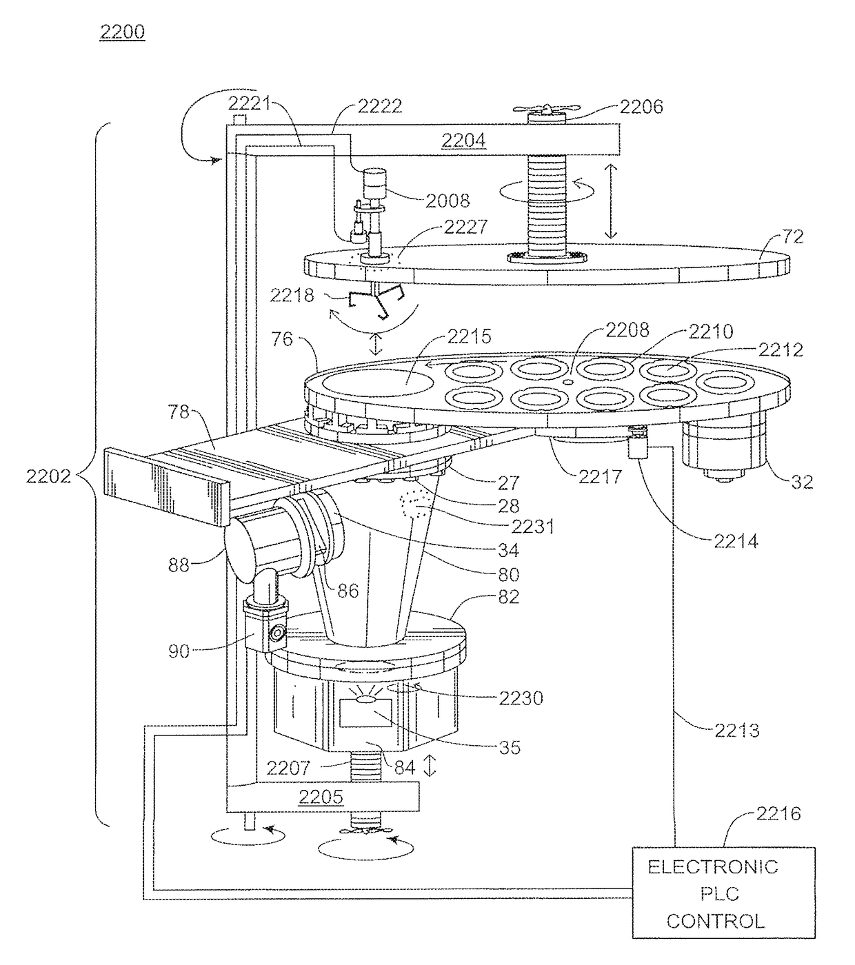
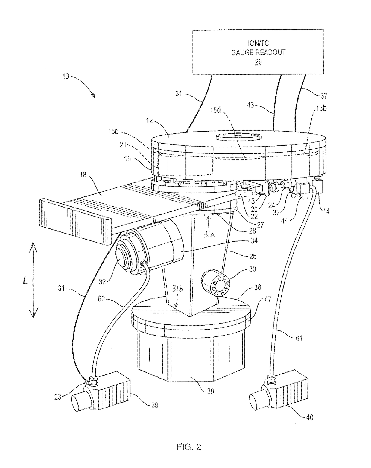
Physical vapor deposition apparatus having a tapered chamber
PatentActiveUS9920418B1
Innovation
- A PVD apparatus with a Tapered Load-Locked Chamber (TLC) configuration, comprising a load-lock deposition chamber, a high vacuum chamber, and a source chamber, utilizing a tapered high vacuum chamber and dual-axis spinning wafer planetary to reduce pump-down time and energy consumption, while allowing for efficient coating of multiple wafers without increasing the apparatus' footprint or energy usage.

Methods and apparatus for physical vapor deposition (PVD) dielectric deposition
PatentWO2021034736A1
Innovation
- A method and apparatus that involve sputtering a dielectric target with a first dielectric constant to form a layer on the inner surface of the shield, which is pre-coated with an aluminum oxide coating having a second dielectric constant similar to the target, reducing the burn-in time and matching the dielectric constants, thereby improving deposition uniformity and reducing processing delays.


Energy Efficiency Standards for PVD Manufacturing
Energy efficiency standards for Physical Vapor Deposition (PVD) manufacturing have emerged as critical regulatory frameworks that directly influence deposition time optimization strategies. These standards establish baseline performance metrics that manufacturers must achieve while maintaining production quality, creating a complex balance between energy consumption and process efficiency.
The International Organization for Standardization (ISO) 14001 environmental management standards and ISO 50001 energy management systems provide foundational frameworks for PVD operations. These standards mandate continuous monitoring of energy consumption per unit of deposited material, establishing key performance indicators that directly correlate with deposition time parameters. Manufacturers must demonstrate measurable improvements in energy efficiency while maintaining coating quality specifications.
Regional energy efficiency regulations vary significantly across major manufacturing hubs. The European Union's Energy Efficiency Directive requires industrial facilities to conduct energy audits every four years, with specific attention to process optimization opportunities. In the United States, the Department of Energy's Better Buildings Challenge encourages voluntary adoption of energy intensity reduction targets, typically ranging from 2.5% to 4% annually for manufacturing processes.
Compliance with these standards necessitates sophisticated process control systems that can dynamically adjust deposition parameters based on real-time energy consumption data. Modern PVD systems integrate power monitoring capabilities that track energy usage across different process phases, enabling operators to identify optimal deposition time windows that minimize energy consumption while achieving target film properties.
The implementation of energy efficiency standards has driven technological innovations in PVD equipment design. Manufacturers now prioritize systems with improved power factor correction, variable frequency drives for pump systems, and advanced thermal management solutions that reduce overall energy requirements. These technological advances enable shorter deposition cycles without compromising film quality, directly supporting deposition time optimization objectives.
Certification programs such as ENERGY STAR for industrial equipment and LEED manufacturing credits provide additional incentives for adopting energy-efficient PVD processes. These programs often require documentation of energy performance improvements, creating systematic approaches to deposition time optimization that align with broader sustainability goals while maintaining competitive manufacturing costs.
Cost-Benefit Analysis of PVD Process Optimization
The cost-benefit analysis of PVD process optimization through deposition time control reveals significant economic advantages across multiple operational dimensions. Initial capital investments in advanced process control systems and real-time monitoring equipment typically range from $200,000 to $500,000 per production line, depending on system complexity and integration requirements. However, these upfront costs are generally recovered within 12-18 months through improved operational efficiency and reduced material waste.
Direct cost savings emerge primarily from enhanced material utilization efficiency. Optimized deposition timing reduces target material consumption by 15-25% while maintaining coating quality specifications. For high-volume production facilities processing precious metals or specialized alloys, this translates to annual savings of $300,000 to $800,000 per production line. Additionally, reduced chamber cleaning frequency and extended component lifespans contribute to lower maintenance costs.
Energy consumption optimization represents another substantial benefit area. Precise deposition time control eliminates unnecessary processing cycles, reducing power consumption by 20-30% during coating operations. Combined with improved chamber utilization rates, facilities typically observe 18-22% reductions in overall energy costs. These savings become particularly significant for operations running multiple shifts or processing large substrate volumes.
Productivity gains through optimized cycle times directly impact manufacturing throughput and labor efficiency. Reduced processing times enable 25-35% increases in daily production capacity without additional equipment investments. This enhanced throughput capability supports revenue growth while distributing fixed costs across larger production volumes, improving overall profit margins.
Quality-related cost benefits include reduced rework rates, lower scrap generation, and improved yield consistency. Optimized deposition parameters minimize coating defects by 40-50%, significantly reducing quality control costs and customer returns. The improved process repeatability also enables tighter specification control, supporting premium product positioning and higher selling prices.
Risk mitigation benefits encompass reduced process variability, improved equipment reliability, and enhanced regulatory compliance. These factors contribute to lower insurance costs, reduced liability exposure, and improved customer satisfaction metrics, providing additional long-term economic value beyond direct operational savings.
Unlock deeper insights with Patsnap Eureka Quick Research — get a full tech report to explore trends and direct your research. Try now!
Generate Your Research Report Instantly with AI Agent
Supercharge your innovation with Patsnap Eureka AI Agent Platform!