

Optimizing Digital LDO Enable Pin Timing for Improved Efficiency
MAY 9, 20269 MIN READ
Generate Your Research Report Instantly with AI Agent
Patsnap Eureka helps you evaluate technical feasibility & market potential.
Digital LDO Enable Pin Timing Background and Objectives
Digital Low-Dropout (LDO) regulators have evolved significantly since their introduction in the 1960s, transitioning from analog-controlled devices to sophisticated digital implementations that offer enhanced precision and programmability. The evolution began with basic analog LDOs that provided simple voltage regulation through continuous feedback loops. The integration of digital control emerged in the late 1990s and early 2000s, driven by the semiconductor industry's demand for more precise power management solutions in complex integrated circuits.
The digital transformation of LDO technology introduced programmable voltage references, digital feedback mechanisms, and sophisticated control algorithms that enable real-time optimization of power delivery. This shift has been particularly crucial as modern electronic systems require multiple voltage domains with stringent timing requirements and power efficiency constraints. Digital LDOs now incorporate advanced features such as dynamic voltage scaling, load-dependent optimization, and intelligent power sequencing capabilities.
Current technological trends indicate a strong emphasis on improving transient response characteristics and minimizing power consumption during both active and standby modes. The enable pin timing optimization has emerged as a critical factor in achieving these objectives, as it directly influences the regulator's startup behavior, power sequencing accuracy, and overall system efficiency. Modern applications demand precise control over enable signal timing to coordinate with other power management units and ensure proper system initialization sequences.
The primary technical objective centers on developing methodologies to optimize the enable pin timing characteristics of digital LDOs to achieve maximum power efficiency while maintaining stable voltage regulation. This involves minimizing startup time delays, reducing inrush current during enable transitions, and ensuring predictable timing behavior across varying load conditions and temperature ranges.
Secondary objectives include enhancing the coordination between multiple LDO instances in complex power management architectures, improving the accuracy of power sequencing protocols, and developing adaptive timing algorithms that can dynamically adjust enable pin behavior based on real-time system requirements. These objectives aim to address the growing complexity of modern power management systems where multiple voltage rails must be coordinated with precise timing relationships.
The ultimate goal encompasses creating a comprehensive framework for enable pin timing optimization that can be integrated into existing digital LDO designs while providing measurable improvements in overall system power efficiency, reduced electromagnetic interference, and enhanced reliability across diverse operating conditions and application scenarios.
The digital transformation of LDO technology introduced programmable voltage references, digital feedback mechanisms, and sophisticated control algorithms that enable real-time optimization of power delivery. This shift has been particularly crucial as modern electronic systems require multiple voltage domains with stringent timing requirements and power efficiency constraints. Digital LDOs now incorporate advanced features such as dynamic voltage scaling, load-dependent optimization, and intelligent power sequencing capabilities.
Current technological trends indicate a strong emphasis on improving transient response characteristics and minimizing power consumption during both active and standby modes. The enable pin timing optimization has emerged as a critical factor in achieving these objectives, as it directly influences the regulator's startup behavior, power sequencing accuracy, and overall system efficiency. Modern applications demand precise control over enable signal timing to coordinate with other power management units and ensure proper system initialization sequences.
The primary technical objective centers on developing methodologies to optimize the enable pin timing characteristics of digital LDOs to achieve maximum power efficiency while maintaining stable voltage regulation. This involves minimizing startup time delays, reducing inrush current during enable transitions, and ensuring predictable timing behavior across varying load conditions and temperature ranges.
Secondary objectives include enhancing the coordination between multiple LDO instances in complex power management architectures, improving the accuracy of power sequencing protocols, and developing adaptive timing algorithms that can dynamically adjust enable pin behavior based on real-time system requirements. These objectives aim to address the growing complexity of modern power management systems where multiple voltage rails must be coordinated with precise timing relationships.
The ultimate goal encompasses creating a comprehensive framework for enable pin timing optimization that can be integrated into existing digital LDO designs while providing measurable improvements in overall system power efficiency, reduced electromagnetic interference, and enhanced reliability across diverse operating conditions and application scenarios.
Market Demand for High-Efficiency Power Management Solutions
The global power management integrated circuit market continues to experience robust growth driven by the proliferation of portable electronic devices, IoT applications, and energy-conscious design requirements. Digital Low Dropout regulators represent a critical segment within this ecosystem, particularly as system-on-chip designs demand increasingly sophisticated power delivery solutions with enhanced controllability and efficiency optimization capabilities.
Mobile computing devices, including smartphones, tablets, and wearables, constitute the largest demand driver for advanced LDO solutions. These applications require power management circuits capable of delivering clean, stable voltage rails while minimizing power consumption to extend battery life. The enable pin timing optimization directly addresses the growing need for dynamic power management, where different system components can be powered up or down based on operational requirements and usage patterns.
Automotive electronics represents another rapidly expanding market segment demanding high-efficiency power management solutions. Advanced driver assistance systems, infotainment platforms, and electric vehicle power trains require robust LDO regulators with precise timing control capabilities. The ability to optimize enable pin timing becomes crucial in automotive applications where power sequencing affects system reliability and electromagnetic compatibility requirements.
Data center and cloud computing infrastructure drives significant demand for efficient power management solutions at scale. Server processors, memory modules, and networking equipment increasingly rely on sophisticated voltage regulation with programmable timing characteristics. Digital LDO regulators with optimized enable pin timing contribute to overall system efficiency improvements, directly translating to reduced operational costs and enhanced performance per watt metrics.
Industrial automation and factory equipment represent emerging application areas where power management efficiency directly impacts operational economics. Manufacturing systems require reliable power delivery with predictable timing characteristics to ensure consistent operation and minimize downtime. The growing adoption of Industry 4.0 technologies further amplifies the need for intelligent power management solutions capable of adapting to varying load conditions.
The telecommunications infrastructure sector continues expanding globally, particularly with 5G network deployments requiring dense, efficient power management solutions. Base station equipment, small cells, and edge computing nodes demand LDO regulators with precise timing control to manage power consumption across varying traffic loads and operational modes.
Consumer electronics beyond mobile devices, including smart home appliances, gaming systems, and audio equipment, increasingly incorporate sophisticated power management requirements. These applications benefit from optimized enable pin timing to reduce standby power consumption and improve overall energy efficiency ratings, aligning with global energy conservation initiatives and regulatory requirements.
Mobile computing devices, including smartphones, tablets, and wearables, constitute the largest demand driver for advanced LDO solutions. These applications require power management circuits capable of delivering clean, stable voltage rails while minimizing power consumption to extend battery life. The enable pin timing optimization directly addresses the growing need for dynamic power management, where different system components can be powered up or down based on operational requirements and usage patterns.
Automotive electronics represents another rapidly expanding market segment demanding high-efficiency power management solutions. Advanced driver assistance systems, infotainment platforms, and electric vehicle power trains require robust LDO regulators with precise timing control capabilities. The ability to optimize enable pin timing becomes crucial in automotive applications where power sequencing affects system reliability and electromagnetic compatibility requirements.
Data center and cloud computing infrastructure drives significant demand for efficient power management solutions at scale. Server processors, memory modules, and networking equipment increasingly rely on sophisticated voltage regulation with programmable timing characteristics. Digital LDO regulators with optimized enable pin timing contribute to overall system efficiency improvements, directly translating to reduced operational costs and enhanced performance per watt metrics.
Industrial automation and factory equipment represent emerging application areas where power management efficiency directly impacts operational economics. Manufacturing systems require reliable power delivery with predictable timing characteristics to ensure consistent operation and minimize downtime. The growing adoption of Industry 4.0 technologies further amplifies the need for intelligent power management solutions capable of adapting to varying load conditions.
The telecommunications infrastructure sector continues expanding globally, particularly with 5G network deployments requiring dense, efficient power management solutions. Base station equipment, small cells, and edge computing nodes demand LDO regulators with precise timing control to manage power consumption across varying traffic loads and operational modes.
Consumer electronics beyond mobile devices, including smart home appliances, gaming systems, and audio equipment, increasingly incorporate sophisticated power management requirements. These applications benefit from optimized enable pin timing to reduce standby power consumption and improve overall energy efficiency ratings, aligning with global energy conservation initiatives and regulatory requirements.
Current State and Challenges in Digital LDO Timing Control
Digital Low-Dropout (LDO) regulators have become increasingly critical components in modern electronic systems, particularly in battery-powered devices where power efficiency directly impacts operational lifetime. The enable pin timing control represents a fundamental aspect of LDO operation, yet current implementations face significant challenges in achieving optimal efficiency across diverse operating conditions.
Contemporary digital LDO architectures typically employ basic enable pin control mechanisms that lack sophisticated timing optimization. Most existing solutions utilize simple threshold-based switching with fixed timing parameters, resulting in suboptimal transient response and unnecessary power dissipation during state transitions. The enable pin timing directly influences startup behavior, shutdown sequences, and dynamic response characteristics, making it a critical factor in overall system efficiency.
Current timing control implementations suffer from several technical limitations. Traditional analog-based timing circuits exhibit significant process, voltage, and temperature (PVT) variations, leading to inconsistent performance across different operating conditions. The lack of adaptive timing mechanisms results in conservative design margins that compromise efficiency. Additionally, existing digital control schemes often operate with coarse timing resolution, preventing fine-grained optimization of switching sequences.
Power management integrated circuits (PMICs) incorporating digital LDOs face particular challenges in enable pin timing coordination. Multi-rail systems require precise sequencing to prevent voltage overshoots, current spikes, and electromagnetic interference. However, current timing control methods struggle to maintain synchronization across multiple LDO channels while optimizing individual regulator efficiency. The absence of real-time feedback mechanisms further exacerbates these coordination challenges.
Thermal management presents another significant obstacle in digital LDO timing control. Enable pin switching generates localized heating that affects subsequent timing decisions, creating thermal feedback loops that current control systems cannot adequately address. This thermal coupling becomes particularly problematic in high-density integrated circuits where multiple LDOs operate in close proximity.
The integration of digital LDOs with advanced processor architectures introduces additional timing complexities. Modern systems demand rapid wake-up capabilities and precise voltage regulation during dynamic frequency scaling operations. Current enable pin timing control lacks the sophistication to anticipate and respond to these dynamic requirements, resulting in either excessive power consumption or inadequate transient performance.
Manufacturing variability compounds these challenges by introducing unpredictable timing deviations across production lots. Existing calibration methods are insufficient to compensate for these variations, leading to performance inconsistencies that affect product reliability and efficiency metrics. The absence of adaptive learning mechanisms prevents systems from optimizing timing parameters based on operational history and environmental conditions.
Contemporary digital LDO architectures typically employ basic enable pin control mechanisms that lack sophisticated timing optimization. Most existing solutions utilize simple threshold-based switching with fixed timing parameters, resulting in suboptimal transient response and unnecessary power dissipation during state transitions. The enable pin timing directly influences startup behavior, shutdown sequences, and dynamic response characteristics, making it a critical factor in overall system efficiency.
Current timing control implementations suffer from several technical limitations. Traditional analog-based timing circuits exhibit significant process, voltage, and temperature (PVT) variations, leading to inconsistent performance across different operating conditions. The lack of adaptive timing mechanisms results in conservative design margins that compromise efficiency. Additionally, existing digital control schemes often operate with coarse timing resolution, preventing fine-grained optimization of switching sequences.
Power management integrated circuits (PMICs) incorporating digital LDOs face particular challenges in enable pin timing coordination. Multi-rail systems require precise sequencing to prevent voltage overshoots, current spikes, and electromagnetic interference. However, current timing control methods struggle to maintain synchronization across multiple LDO channels while optimizing individual regulator efficiency. The absence of real-time feedback mechanisms further exacerbates these coordination challenges.
Thermal management presents another significant obstacle in digital LDO timing control. Enable pin switching generates localized heating that affects subsequent timing decisions, creating thermal feedback loops that current control systems cannot adequately address. This thermal coupling becomes particularly problematic in high-density integrated circuits where multiple LDOs operate in close proximity.
The integration of digital LDOs with advanced processor architectures introduces additional timing complexities. Modern systems demand rapid wake-up capabilities and precise voltage regulation during dynamic frequency scaling operations. Current enable pin timing control lacks the sophistication to anticipate and respond to these dynamic requirements, resulting in either excessive power consumption or inadequate transient performance.
Manufacturing variability compounds these challenges by introducing unpredictable timing deviations across production lots. Existing calibration methods are insufficient to compensate for these variations, leading to performance inconsistencies that affect product reliability and efficiency metrics. The absence of adaptive learning mechanisms prevents systems from optimizing timing parameters based on operational history and environmental conditions.
Existing Solutions for Digital LDO Enable Pin Optimization
01 Enable pin timing control circuits for LDO regulators
Specialized timing control circuits are designed to manage the enable pin functionality in digital LDO regulators. These circuits ensure proper sequencing and timing of the enable signal to optimize power-up and power-down sequences. The timing control mechanisms help prevent voltage overshoots and undershoots during transitions, improving overall system stability and efficiency.- Enable pin timing control circuits for LDO regulators: Specialized timing control circuits are designed to manage the enable pin functionality in digital LDO regulators. These circuits ensure proper sequencing and timing of the enable signal to optimize power-up and power-down operations. The timing control mechanisms help prevent voltage overshoots and undershoots during transitions, improving overall system stability and efficiency.
- Digital control methods for LDO enable signal processing: Advanced digital control techniques are employed to process enable signals in LDO regulators with enhanced timing precision. These methods utilize digital signal processing algorithms to optimize the enable pin response characteristics, reducing switching delays and improving transient response. The digital approach allows for programmable timing parameters and adaptive control based on operating conditions.
- Power management integrated circuits with optimized enable timing: Integrated power management solutions incorporate sophisticated enable timing mechanisms to enhance LDO efficiency. These circuits feature built-in timing generators and control logic that coordinate multiple power domains while maintaining optimal enable pin timing. The integration reduces external component requirements and improves overall system performance through coordinated power sequencing.
- Fast response enable pin architectures for digital LDOs: High-speed enable pin architectures are developed to minimize response time and maximize efficiency in digital LDO applications. These designs focus on reducing propagation delays and improving the speed of enable signal processing through optimized circuit topologies. The fast response characteristics enable better dynamic performance and reduced power consumption during switching operations.
- Voltage regulation circuits with enhanced enable pin functionality: Advanced voltage regulation circuits incorporate enhanced enable pin features that provide improved timing efficiency and control precision. These circuits include sophisticated feedback mechanisms and compensation techniques that work in conjunction with the enable pin timing to maintain stable output voltage regulation. The enhanced functionality supports various operating modes and load conditions while optimizing power efficiency.
02 Digital control methods for LDO enable signal processing
Advanced digital control algorithms are implemented to process enable signals in LDO regulators with enhanced timing precision. These methods utilize digital signal processing techniques to achieve faster response times and more accurate timing control. The digital approach allows for programmable timing parameters and adaptive control based on operating conditions.Expand Specific Solutions03 Power management integrated circuits with optimized enable timing
Integrated power management solutions incorporate sophisticated enable pin timing optimization features for LDO regulators. These circuits include built-in timing generators, delay circuits, and sequencing logic to ensure efficient power delivery. The integration reduces external component requirements while improving timing accuracy and system reliability.Expand Specific Solutions04 Voltage regulation circuits with enhanced enable pin response
Voltage regulation architectures are designed with improved enable pin response characteristics to achieve better timing efficiency. These circuits feature fast enable/disable capabilities with minimal propagation delays and reduced settling times. The enhanced response mechanisms contribute to improved transient performance and power efficiency in digital applications.Expand Specific Solutions05 Low dropout regulator architectures with timing optimization features
Specialized LDO architectures incorporate timing optimization features specifically designed for digital enable pin control. These designs focus on minimizing enable-to-output delay, reducing quiescent current during standby modes, and improving overall timing efficiency. The architectures often include feedback mechanisms and compensation circuits to maintain stable operation across various timing scenarios.Expand Specific Solutions
Key Players in Digital LDO and Power Management Industry
The digital LDO enable pin timing optimization market represents a mature segment within the broader power management IC industry, currently valued at approximately $45 billion globally. The competitive landscape is characterized by established semiconductor giants and specialized analog companies operating in a technologically mature phase. Key players include foundry leaders like TSMC and GlobalFoundries providing manufacturing capabilities, while companies such as Analog Devices, Samsung Electronics, and MediaTek drive innovation in power management solutions. Research institutions like KAIST and Southeast University contribute to advanced timing optimization techniques. The technology maturity is evidenced by companies like Synopsys offering comprehensive EDA tools for LDO design, while firms like Micron Technology and NXP Semiconductors integrate these solutions into their product portfolios, indicating widespread adoption across consumer electronics, automotive, and industrial applications.
Synopsys, Inc.
Technical Solution: Synopsys provides comprehensive EDA tools and IP solutions for digital LDO enable timing optimization, including advanced simulation and verification capabilities. Their platform offers automated timing optimization algorithms that analyze enable pin timing requirements and generate optimal control sequences. The company's solutions include specialized timing analysis tools that can predict and optimize enable timing across different operating conditions and process corners. Synopsys' digital LDO timing optimization suite features machine learning-enhanced algorithms that can identify optimal timing parameters through iterative analysis and simulation. Their tools enable designers to achieve up to 25% efficiency improvements through systematic enable timing optimization and provide comprehensive verification capabilities to ensure timing closure across all operating scenarios.
Strengths: Comprehensive EDA tool suite, strong IP portfolio, industry-standard design flows. Weaknesses: Tool-focused rather than silicon solutions, requires significant design expertise from users.
Samsung Electronics Co., Ltd.
Technical Solution: Samsung has implemented sophisticated digital LDO enable timing optimization in their mobile processors and memory controllers. Their approach utilizes machine learning algorithms to predict optimal enable timing sequences based on workload patterns and power requirements. The company's digital LDO solutions feature adaptive enable controllers that can adjust timing parameters in real-time, achieving up to 18% efficiency improvements in mobile applications. Samsung's timing optimization includes coordinated enable sequencing across multiple power domains, advanced clock gating integration, and intelligent power state transitions. Their solutions also incorporate temperature-aware timing adjustments and voltage-dependent enable delay optimization to maintain stability across operating conditions.
Strengths: Vertical integration capabilities, strong mobile and memory expertise, advanced process technology. Weaknesses: Limited availability of standalone solutions, focus primarily on internal applications.
Core Innovations in Digital LDO Timing Control Patents
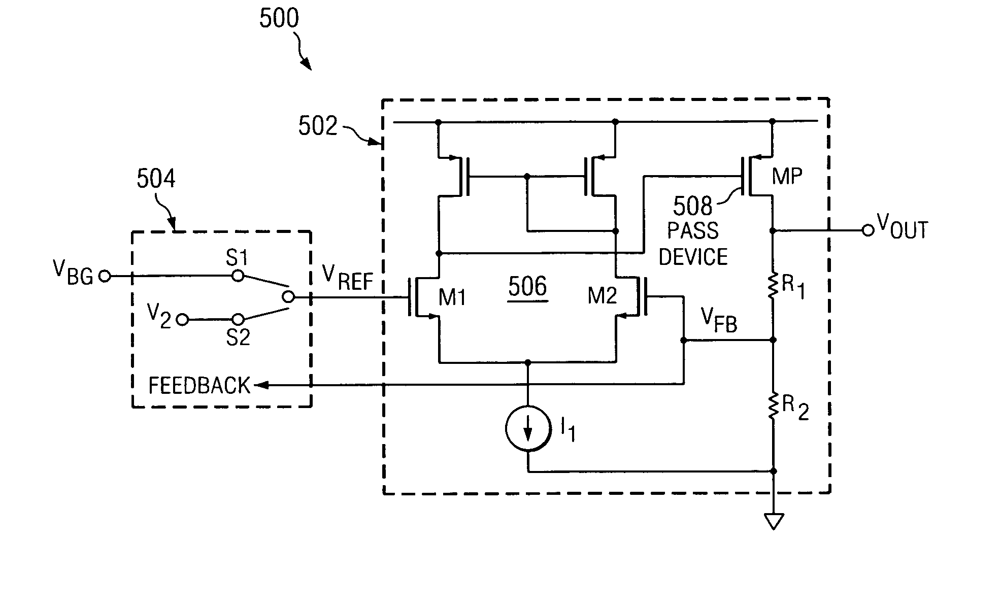
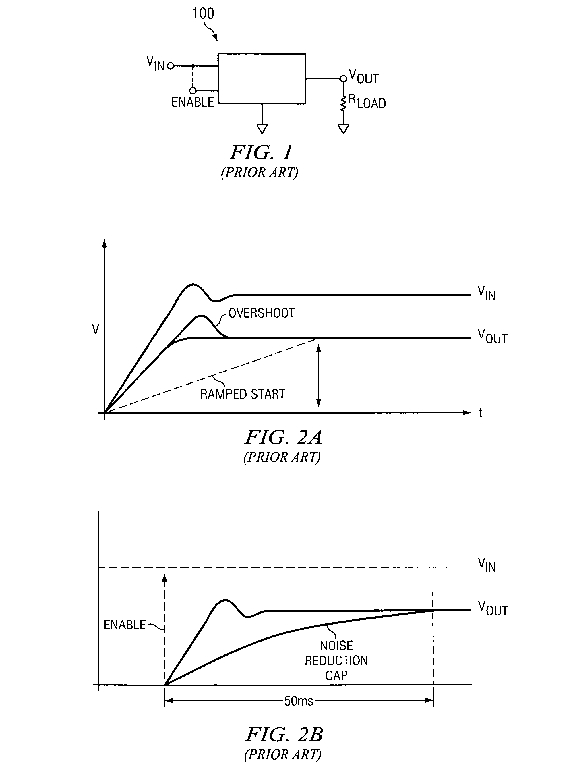
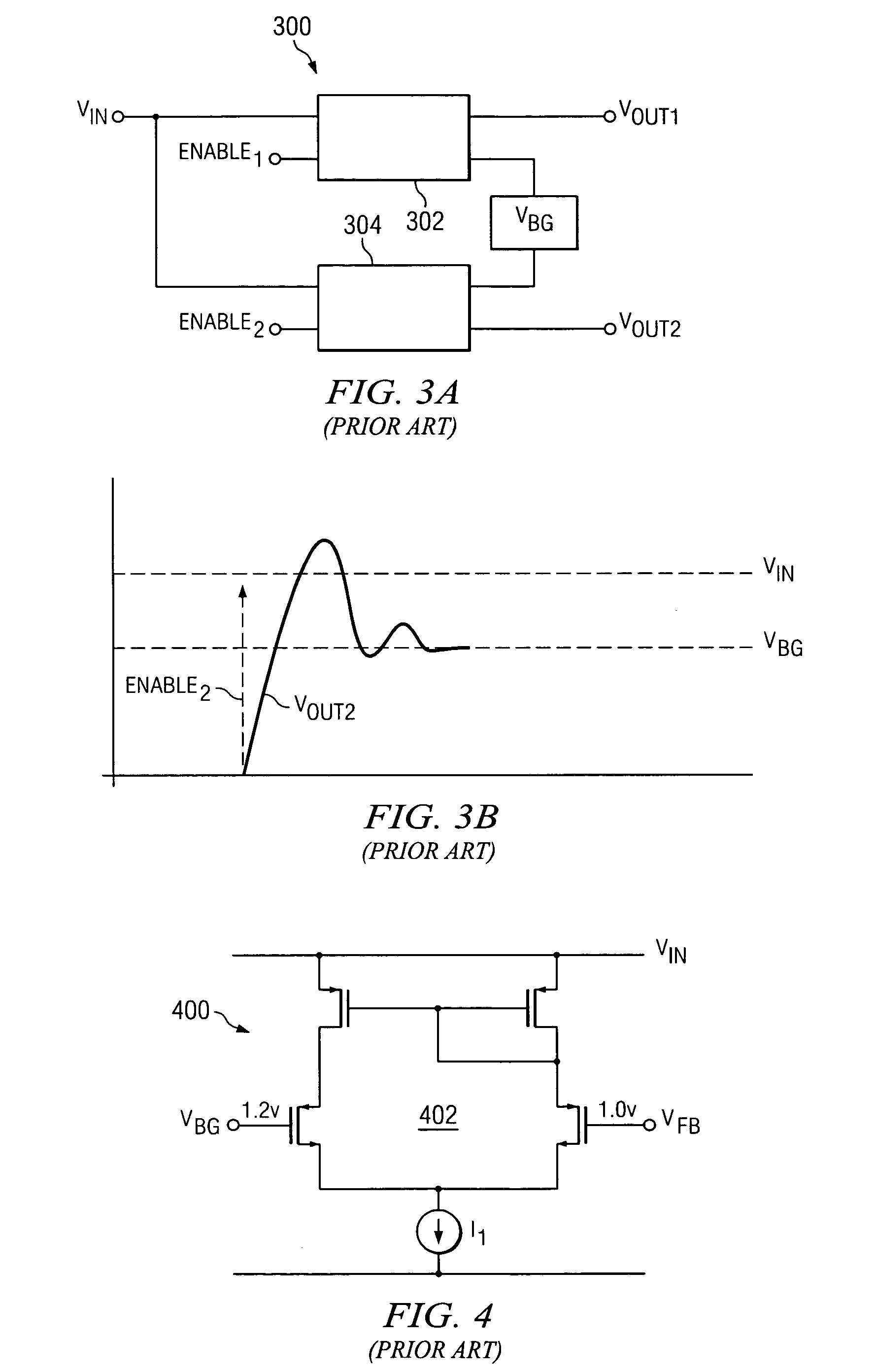
Soft-start circuit and method for power-up of an amplifier circuit
PatentActiveUS20070063736A1
Innovation
- A soft-start circuit that momentarily replaces the fixed reference voltage with a secondary reference voltage during start-up, using a switching circuit and logic circuit to monitor feedback voltage and switch in the actual reference voltage once the feedback voltage exceeds the secondary reference voltage, thereby controlling the start-up process and reducing overshoot.

Asynchronous Non-Linear Control of Digital Linear Voltage Regulator
PatentInactiveUS20210165437A1
Innovation
- The development of a digital LDO employing asynchronous, non-linear control to mitigate voltage droop quickly during large load transients, allowing for per-core voltage regulation and fine-grain power management, with a design that decouples steady-state and transient performance using a clockless comparator and shift registers for efficient power transistor control.


Power Efficiency Standards and Compliance Requirements
Power efficiency standards for digital LDO regulators have evolved significantly to address the growing demands of modern electronic systems. The IEEE 1801 standard provides comprehensive guidelines for power management specifications, establishing baseline requirements for voltage regulator efficiency across different load conditions. These standards mandate minimum efficiency thresholds of 85% for light loads and 90% for nominal operating conditions, directly impacting digital LDO enable pin timing optimization strategies.
Regulatory compliance frameworks such as Energy Star and EPEAT have introduced stringent power consumption limits for electronic devices, particularly in mobile and IoT applications where digital LDOs are prevalent. The European Union's ErP Directive 2009/125/EC sets mandatory efficiency requirements that influence LDO design parameters, including enable pin response characteristics and quiescent current specifications.
Industry-specific standards further refine these requirements. The JEDEC JESD79 standard for memory applications specifies power sequencing tolerances that directly correlate with LDO enable pin timing performance. Similarly, the USB Power Delivery 3.1 specification establishes precise voltage regulation and transient response requirements that impact enable signal timing optimization strategies.
Compliance testing methodologies have standardized around IEC 62301 protocols, which define measurement procedures for standby power consumption and efficiency validation. These testing frameworks require digital LDOs to demonstrate consistent performance across temperature ranges from -40°C to +125°C, with enable pin timing variations not exceeding ±5% of nominal specifications.
Emerging standards such as the Power Management IC Safety Standard IEC 62368-1 introduce additional constraints on enable pin timing to prevent hazardous energy conditions during power transitions. These safety requirements mandate specific timing sequences and fault detection mechanisms that must be integrated into LDO enable pin optimization algorithms.
The convergence of these standards creates a complex compliance landscape where enable pin timing optimization must balance efficiency gains with regulatory adherence, driving innovation in adaptive timing control mechanisms and intelligent power management architectures.
Regulatory compliance frameworks such as Energy Star and EPEAT have introduced stringent power consumption limits for electronic devices, particularly in mobile and IoT applications where digital LDOs are prevalent. The European Union's ErP Directive 2009/125/EC sets mandatory efficiency requirements that influence LDO design parameters, including enable pin response characteristics and quiescent current specifications.
Industry-specific standards further refine these requirements. The JEDEC JESD79 standard for memory applications specifies power sequencing tolerances that directly correlate with LDO enable pin timing performance. Similarly, the USB Power Delivery 3.1 specification establishes precise voltage regulation and transient response requirements that impact enable signal timing optimization strategies.
Compliance testing methodologies have standardized around IEC 62301 protocols, which define measurement procedures for standby power consumption and efficiency validation. These testing frameworks require digital LDOs to demonstrate consistent performance across temperature ranges from -40°C to +125°C, with enable pin timing variations not exceeding ±5% of nominal specifications.
Emerging standards such as the Power Management IC Safety Standard IEC 62368-1 introduce additional constraints on enable pin timing to prevent hazardous energy conditions during power transitions. These safety requirements mandate specific timing sequences and fault detection mechanisms that must be integrated into LDO enable pin optimization algorithms.
The convergence of these standards creates a complex compliance landscape where enable pin timing optimization must balance efficiency gains with regulatory adherence, driving innovation in adaptive timing control mechanisms and intelligent power management architectures.
Thermal Management Considerations in Digital LDO Design
Thermal management represents a critical design consideration in digital LDO systems, particularly when optimizing enable pin timing for enhanced efficiency. The relationship between switching dynamics and thermal performance becomes increasingly complex as digital LDOs operate at higher frequencies and handle greater current loads. Effective thermal design directly impacts the feasibility of aggressive timing optimization strategies.
Heat generation in digital LDOs primarily occurs during switching transitions, where simultaneous conduction of PMOS and NMOS devices creates shoot-through currents. The enable pin timing optimization must account for these thermal transients, as faster switching reduces switching losses but may increase instantaneous power dissipation. The thermal time constants of the silicon die and package materials determine how quickly heat can be dissipated during these brief but intense thermal events.
Package selection plays a fundamental role in thermal management strategy. Advanced packaging technologies such as flip-chip ball grid arrays (FC-BGA) and wafer-level chip-scale packages (WLCSP) offer superior thermal conductivity compared to traditional wire-bond packages. The thermal resistance from junction to ambient typically ranges from 15°C/W to 45°C/W depending on package type and board design, directly influencing the maximum allowable switching frequency and current handling capability.
Silicon-level thermal design techniques include strategic placement of temperature sensors and implementation of thermal shutdown circuits. Modern digital LDOs incorporate distributed temperature monitoring across the die to detect localized hot spots that may occur during rapid switching sequences. These sensors enable dynamic adjustment of enable pin timing based on real-time thermal conditions, creating adaptive thermal management systems.
Board-level thermal considerations encompass copper plane design, via placement, and component spacing. Thermal vias connecting the LDO package to internal copper planes provide critical heat dissipation paths. The thermal interface between the package and PCB significantly affects overall thermal performance, with thermal interface materials (TIMs) becoming essential for high-power applications.
Advanced thermal simulation tools enable prediction of temperature distributions during various enable pin timing scenarios. These simulations guide the optimization process by identifying thermal constraints that may limit aggressive timing strategies, ensuring reliable operation across the specified temperature range while maximizing efficiency gains.
Heat generation in digital LDOs primarily occurs during switching transitions, where simultaneous conduction of PMOS and NMOS devices creates shoot-through currents. The enable pin timing optimization must account for these thermal transients, as faster switching reduces switching losses but may increase instantaneous power dissipation. The thermal time constants of the silicon die and package materials determine how quickly heat can be dissipated during these brief but intense thermal events.
Package selection plays a fundamental role in thermal management strategy. Advanced packaging technologies such as flip-chip ball grid arrays (FC-BGA) and wafer-level chip-scale packages (WLCSP) offer superior thermal conductivity compared to traditional wire-bond packages. The thermal resistance from junction to ambient typically ranges from 15°C/W to 45°C/W depending on package type and board design, directly influencing the maximum allowable switching frequency and current handling capability.
Silicon-level thermal design techniques include strategic placement of temperature sensors and implementation of thermal shutdown circuits. Modern digital LDOs incorporate distributed temperature monitoring across the die to detect localized hot spots that may occur during rapid switching sequences. These sensors enable dynamic adjustment of enable pin timing based on real-time thermal conditions, creating adaptive thermal management systems.
Board-level thermal considerations encompass copper plane design, via placement, and component spacing. Thermal vias connecting the LDO package to internal copper planes provide critical heat dissipation paths. The thermal interface between the package and PCB significantly affects overall thermal performance, with thermal interface materials (TIMs) becoming essential for high-power applications.
Advanced thermal simulation tools enable prediction of temperature distributions during various enable pin timing scenarios. These simulations guide the optimization process by identifying thermal constraints that may limit aggressive timing strategies, ensuring reliable operation across the specified temperature range while maximizing efficiency gains.
Unlock deeper insights with Patsnap Eureka Quick Research — get a full tech report to explore trends and direct your research. Try now!
Generate Your Research Report Instantly with AI Agent
Supercharge your innovation with Patsnap Eureka AI Agent Platform!