

Improving Digital LDO Stability with Capacitor Layout Optimization
MAY 9, 20269 MIN READ
Generate Your Research Report Instantly with AI Agent
PatSnap Eureka helps you evaluate technical feasibility & market potential.
Digital LDO Stability Background and Technical Objectives
Digital Low-Dropout (LDO) regulators have evolved significantly since their inception in the 1970s, transitioning from purely analog designs to sophisticated digital implementations that offer enhanced programmability and integration capabilities. The fundamental principle of LDO operation involves maintaining a stable output voltage despite variations in input voltage and load current through continuous feedback control. Traditional analog LDOs utilize operational amplifiers and pass transistors to achieve regulation, while digital LDOs incorporate digital control loops, pulse-width modulation, and advanced feedback mechanisms to enhance performance metrics.
The evolution toward digital LDO architectures has been driven by the increasing demand for power management solutions in System-on-Chip (SoC) applications, where multiple voltage domains require precise regulation with minimal area overhead. Digital LDOs offer superior process scalability, reduced design complexity in advanced CMOS nodes, and enhanced integration with digital control systems. However, this transition has introduced new challenges related to stability, particularly concerning loop dynamics and transient response characteristics.
Stability in digital LDO systems represents a critical design parameter that directly impacts system reliability and performance. Unlike analog counterparts, digital LDOs face unique stability challenges arising from quantization effects, sampling delays, and discrete-time control mechanisms. The stability margin determines the regulator's ability to maintain consistent output voltage under varying load conditions while preventing oscillations that could compromise system functionality.
Capacitor layout optimization has emerged as a pivotal factor in achieving optimal digital LDO stability. The physical arrangement, sizing, and placement of decoupling and compensation capacitors significantly influence the frequency response characteristics and phase margins of the control loop. Parasitic inductances and resistances introduced by suboptimal layout practices can create unwanted poles and zeros in the transfer function, potentially leading to instability or degraded transient performance.
The primary technical objective focuses on developing systematic methodologies for capacitor layout optimization that enhance digital LDO stability margins while maintaining compact silicon area requirements. This involves establishing design guidelines for capacitor placement relative to the pass device and control circuitry, optimizing interconnect routing to minimize parasitic effects, and implementing layout techniques that improve power supply rejection ratio and load transient response.
Secondary objectives include developing predictive models that correlate layout parameters with stability metrics, enabling designers to evaluate stability implications during the layout phase. Additionally, the research aims to establish trade-off relationships between layout optimization, silicon area utilization, and manufacturing yield considerations, ensuring practical applicability in commercial IC development environments.
Market Demand for High-Performance Digital LDO Solutions
The semiconductor industry is experiencing unprecedented demand for high-performance digital Low Dropout Regulators (LDOs) driven by the proliferation of advanced electronic systems requiring precise power management. Modern applications spanning artificial intelligence processors, 5G infrastructure, automotive electronics, and Internet of Things devices necessitate power regulation solutions that deliver exceptional stability, fast transient response, and minimal noise characteristics.
Digital LDOs have emerged as critical components in System-on-Chip architectures where multiple voltage domains require independent regulation with tight voltage tolerances. The increasing complexity of integrated circuits, particularly in advanced process nodes below 7nm, has amplified the importance of power supply integrity. Applications demanding high computational performance while maintaining energy efficiency create substantial market pull for digital LDO solutions that can dynamically adjust to varying load conditions.
The automotive sector represents a particularly robust growth driver, with electric vehicles and autonomous driving systems requiring reliable power management under extreme operating conditions. These applications demand digital LDOs capable of maintaining stability across wide temperature ranges while supporting rapid load transients from processors, sensors, and communication modules.
Data center and cloud computing infrastructure constitute another significant market segment, where power efficiency directly impacts operational costs and environmental sustainability. High-performance digital LDOs enable fine-grained power management in server processors and memory subsystems, contributing to overall system efficiency improvements.
Mobile and portable device markets continue expanding, with consumers expecting longer battery life and faster performance from smartphones, tablets, and wearable devices. Digital LDOs supporting multiple voltage rails with minimal quiescent current consumption address these requirements while enabling compact form factors.
The growing adoption of edge computing and artificial intelligence accelerators in various applications creates additional demand for specialized power management solutions. These systems require digital LDOs capable of supporting high-frequency switching loads while maintaining voltage regulation accuracy essential for reliable operation of sensitive analog and mixed-signal circuits.
Market dynamics indicate sustained growth in demand for digital LDO solutions that can address stability challenges through innovative design approaches, including optimized capacitor layouts that enhance transient response and reduce output voltage variations across diverse operating conditions.
Current Digital LDO Stability Issues and Layout Challenges
Digital Low-Dropout (LDO) regulators face significant stability challenges that directly impact their performance in modern electronic systems. The primary stability concern stems from the inherent feedback loop dynamics, where phase margin degradation can lead to oscillations and poor transient response. Traditional analog LDOs rely on compensation capacitors and careful loop design, but digital LDOs introduce additional complexity through quantization effects and discrete-time control mechanisms.
The quantization noise inherent in digital control systems creates a fundamental stability challenge. Unlike analog LDOs with continuous feedback, digital variants operate with discrete voltage steps determined by the resolution of their digital-to-analog converters. This quantization introduces limit cycle oscillations and can cause the output voltage to hunt around the target value, particularly under light load conditions where the feedback sensitivity is highest.
Loop delay presents another critical stability issue in digital LDO architectures. The digital control path introduces multiple clock cycle delays through analog-to-digital conversion, digital processing, and digital-to-analog conversion stages. These delays shift the phase response and can push the system toward instability, especially at higher switching frequencies where the delay becomes a significant fraction of the control period.
Capacitor layout optimization emerges as a crucial factor in addressing these stability challenges. The physical placement and routing of decoupling capacitors directly affects the parasitic inductance and resistance in the power delivery path. Poor layout practices can introduce unwanted poles and zeros in the transfer function, degrading phase margin and potentially causing high-frequency oscillations.
The effective series resistance (ESR) and effective series inductance (ESL) of capacitors become particularly problematic in digital LDO applications. High ESL can create resonant peaks that interact with the digital control loop, while inadequate ESR can remove beneficial damping. The layout must carefully balance these parasitic elements to maintain stability across varying load conditions.
Ground bounce and supply noise coupling through inadequate layout practices further exacerbate stability issues. Digital switching activities can couple into the analog feedback path through shared ground impedances or inadequate power supply decoupling. This coupling can trigger false feedback responses and destabilize the regulation loop.
Temperature and process variations add another layer of complexity to digital LDO stability. The discrete nature of digital control makes these systems more sensitive to component variations that affect the loop characteristics. Layout optimization must account for these variations to ensure robust stability across all operating conditions and manufacturing tolerances.
Existing Capacitor Layout Solutions for LDO Stability
01 Digital control loop compensation techniques
Digital LDO regulators employ advanced control loop compensation methods to maintain stability across varying load conditions. These techniques include digital PID controllers, adaptive compensation algorithms, and predictive control methods that adjust the feedback loop parameters in real-time to prevent oscillations and ensure stable output voltage regulation.- Digital control loop compensation techniques: Digital LDO regulators employ advanced control loop compensation methods to maintain stability across varying load conditions. These techniques include digital PID controllers, adaptive compensation algorithms, and predictive control schemes that adjust the regulator's response in real-time. The digital implementation allows for precise tuning of compensation parameters and enables complex control strategies that are difficult to achieve with analog circuits.
- Load transient response optimization: Stability enhancement in digital LDOs focuses on improving transient response during rapid load changes. This involves implementing fast detection circuits, predictive load sensing, and dynamic bandwidth adjustment mechanisms. The digital architecture enables sophisticated algorithms that can anticipate load variations and preemptively adjust the output to minimize voltage droops and overshoots.
- Digital feedback and error correction systems: Advanced digital feedback mechanisms are employed to ensure precise voltage regulation and system stability. These systems utilize high-resolution analog-to-digital converters, digital signal processing algorithms, and error correction techniques to maintain accurate output voltage control. The digital approach allows for complex feedback strategies including multi-loop control and adaptive filtering.
- Power management and efficiency optimization: Digital LDO stability is enhanced through intelligent power management techniques that optimize efficiency while maintaining regulation performance. These methods include dynamic voltage scaling, adaptive biasing, and smart power sequencing. The digital control enables real-time monitoring of power consumption and automatic adjustment of operating parameters to achieve optimal efficiency without compromising stability.
- Temperature and process variation compensation: Digital LDO regulators incorporate sophisticated compensation mechanisms to maintain stability across temperature variations and process corners. These techniques include digital temperature sensing, adaptive reference generation, and process-aware calibration algorithms. The digital implementation allows for precise characterization and real-time adjustment of circuit parameters to ensure consistent performance across all operating conditions.
02 Load transient response optimization
Stability enhancement through improved load transient response involves implementing fast-response digital control algorithms and dynamic current sensing mechanisms. These approaches enable rapid detection of load changes and quick adjustment of the regulation loop to minimize voltage droops and overshoots during transient events.Expand Specific Solutions03 Digital feedback and error correction systems
Advanced digital feedback mechanisms incorporate error detection and correction algorithms to maintain LDO stability. These systems utilize digital signal processing techniques, multi-bit ADCs for precise voltage monitoring, and sophisticated error amplification methods to achieve accurate voltage regulation with minimal noise and improved stability margins.Expand Specific Solutions04 Power supply rejection and noise immunity
Digital LDO stability is enhanced through improved power supply rejection ratio techniques and noise immunity mechanisms. These include digital filtering algorithms, supply voltage feedforward compensation, and adaptive bandwidth control that automatically adjusts the regulator's response to supply variations and external noise sources.Expand Specific Solutions05 Temperature and process variation compensation
Stability across temperature and process variations is achieved through digital calibration and compensation techniques. These methods include temperature coefficient correction algorithms, process corner detection and adjustment, and adaptive biasing schemes that maintain consistent performance and stability across different operating conditions and manufacturing variations.Expand Specific Solutions
Key Players in Digital LDO and Power Management IC Industry
The digital LDO stability improvement through capacitor layout optimization represents a rapidly evolving segment within the broader power management IC market, currently valued at approximately $40 billion globally. The industry is in a mature growth phase, driven by increasing demand for efficient power solutions in mobile devices, IoT applications, and automotive electronics. Technology maturity varies significantly across market participants, with established semiconductor giants like Texas Instruments, Infineon Technologies, Qualcomm, and Samsung Display leading in advanced implementation capabilities. Asian companies including SK Hynix, GigaDevice Semiconductor, and Renesas Design demonstrate strong technical competencies, while research institutions such as University of Electronic Science & Technology of China, Hong Kong University of Science & Technology, and Indian Institute of Technology Madras contribute fundamental research breakthroughs. The competitive landscape shows consolidation around companies with comprehensive analog design expertise and advanced process technologies, positioning digital LDO optimization as a critical differentiator in next-generation power management solutions.
Texas Instruments Incorporated
Technical Solution: Texas Instruments has developed advanced digital LDO architectures with integrated capacitor layout optimization techniques. Their approach focuses on minimizing parasitic inductance and resistance through strategic placement of decoupling capacitors in close proximity to the LDO output stage. The company employs multi-layer PCB design methodologies with dedicated power and ground planes to reduce noise coupling. Their digital LDO controllers incorporate adaptive feedback compensation that accounts for capacitor ESR variations across temperature and frequency ranges. TI's solutions feature programmable output voltage regulation with fast transient response capabilities, utilizing optimized capacitor networks that maintain stability margins above 60 degrees phase margin across all operating conditions.
Strengths: Extensive analog design expertise, comprehensive simulation tools, proven track record in power management ICs. Weaknesses: Higher cost compared to discrete solutions, limited customization options for specialized applications.
Renesas Design (UK) Ltd.
Technical Solution: Renesas has developed comprehensive digital LDO stability enhancement solutions through systematic capacitor layout optimization approaches. Their methodology combines traditional analog design principles with modern digital control techniques to achieve optimal stability performance across varying load conditions. The company's approach utilizes advanced SPICE modeling and electromagnetic simulation tools to characterize parasitic effects and optimize capacitor placement strategies. Renesas implements multi-phase digital LDO architectures with distributed capacitor networks that provide enhanced transient response and improved stability margins. Their solutions feature programmable compensation networks and adaptive control algorithms that maintain stability across process, voltage, and temperature variations. The capacitor layout optimization includes consideration of package parasitic effects, board-level routing constraints, and thermal management requirements for automotive and industrial applications.
Strengths: Strong automotive and industrial market presence, comprehensive analog and digital design capabilities, proven reliability. Weaknesses: Limited presence in high-performance computing markets, longer development cycles compared to specialized competitors.
Core Innovations in Digital LDO Capacitor Layout Design
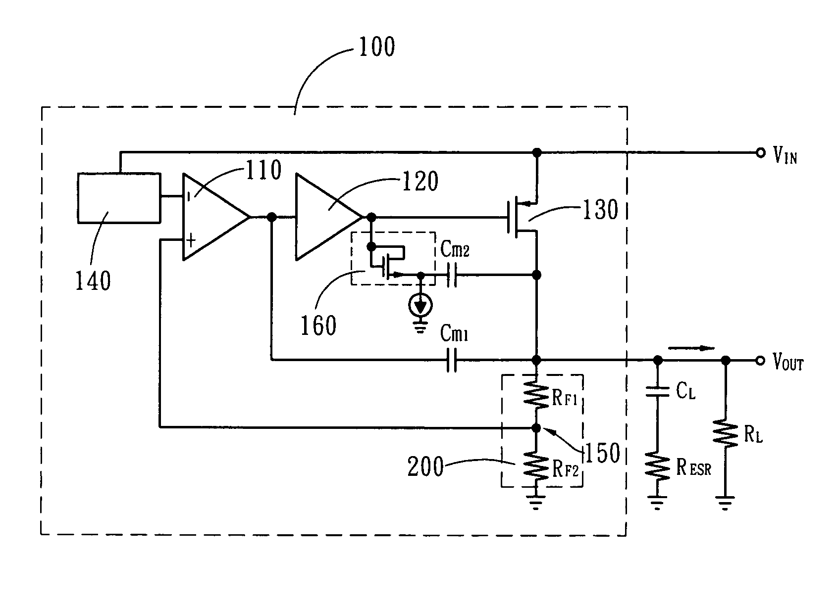
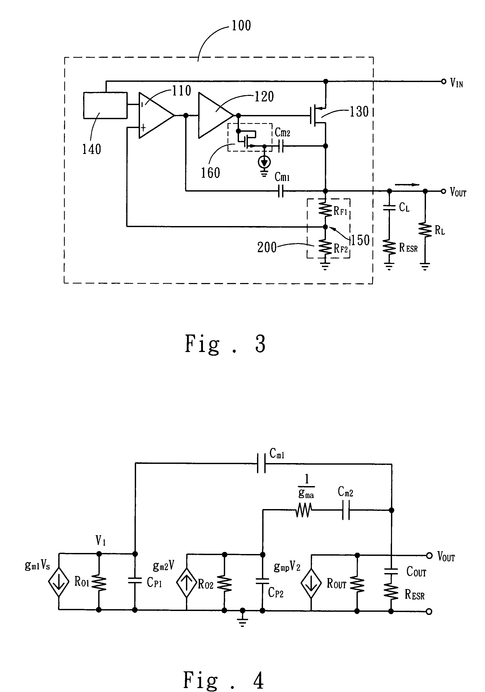
Low dropout linear voltage regulator with an active resistance for frequency compensation to improve stability
PatentInactiveUS7710091B2
Innovation
- The use of nested Miller compensation with pole-splitting and the addition of an active resistor in the feedback path, along with a capacitor-sharing technique to reduce Miller capacitance, allows for superior stability without large output capacitors and enhances damping factor control, extending bandwidth and accelerating voltage stabilization.
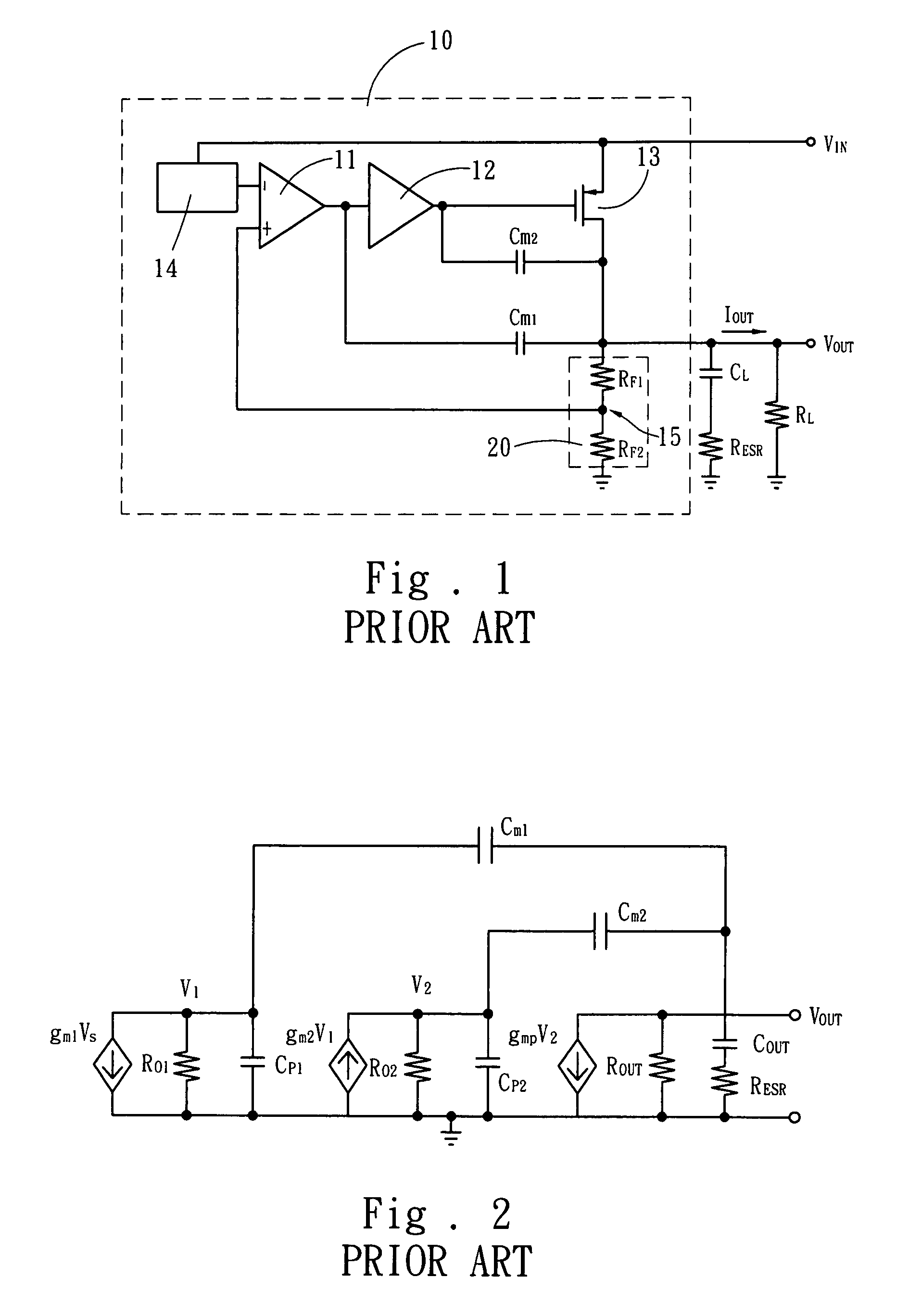

Low dropout regulator with stability compensation circuit
PatentInactiveUS7902801B2
Innovation
- A low dropout voltage regulator with a stability compensation circuit that includes a voltage dependent compensation capacitor and a parasitic pole reshaping PMOS transistor, which adjusts capacitance with load current to track the second pole and maintain a good phase margin, reducing power consumption and eliminating ESR dependence.


EMI/EMC Compliance Requirements for Power Management ICs
Digital Low-Dropout (LDO) regulators in power management integrated circuits must comply with stringent electromagnetic interference (EMI) and electromagnetic compatibility (EMC) standards to ensure reliable operation in complex electronic environments. The primary regulatory frameworks governing these requirements include CISPR 25 for automotive applications, FCC Part 15 for consumer electronics, and IEC 61000 series for industrial applications. These standards define acceptable limits for conducted and radiated emissions while establishing immunity thresholds against external electromagnetic disturbances.
Conducted emissions represent a critical compliance challenge for digital LDOs, particularly in the frequency range of 150 kHz to 30 MHz. The switching nature of digital control loops generates harmonic content that can propagate through power supply lines and ground connections. Regulatory limits typically restrict conducted emissions to levels below 66-56 dBμV across this frequency spectrum, with automotive applications requiring even stricter limits of 46-36 dBμV. The capacitor layout optimization directly impacts these conducted emission levels by influencing current loop areas and parasitic inductances.
Radiated emissions compliance focuses on the 30 MHz to 1 GHz frequency range, where digital LDO switching frequencies and their harmonics can create significant electromagnetic field radiation. Class B limits for consumer applications restrict radiated emissions to 40 dBμV/m at 3 meters for frequencies above 30 MHz, while Class A industrial limits allow 46 dBμV/m. The physical arrangement of decoupling capacitors and their connection paths significantly affects the antenna-like behavior of circuit traces and component leads.
Immunity requirements ensure digital LDOs maintain stable operation despite external electromagnetic interference. Key immunity tests include electrostatic discharge (ESD) up to 8 kV contact discharge, radio frequency interference (RFI) with field strengths up to 10 V/m, and conducted immunity tests with injection levels reaching 10 V. Proper capacitor placement and grounding strategies are essential for maintaining regulation accuracy and preventing oscillations during these disturbance events.
Compliance verification requires comprehensive testing using calibrated equipment in accredited facilities. Pre-compliance testing during development phases helps identify potential issues early, while final certification testing validates conformance to applicable standards. The capacitor layout optimization strategy must consider these EMI/EMC requirements from the initial design phase to avoid costly redesigns and ensure successful regulatory approval for commercial deployment.
Thermal Management Considerations in Digital LDO Design
Thermal management represents a critical design consideration in digital LDO circuits, particularly when implementing capacitor layout optimization strategies for stability enhancement. The inherent switching nature of digital LDOs generates significant heat dissipation, which directly impacts both the performance of output capacitors and overall system stability. Temperature variations affect capacitor characteristics, including equivalent series resistance (ESR) and capacitance values, thereby influencing the feedback loop dynamics and transient response performance.
The placement of output capacitors in relation to heat-generating components requires careful thermal analysis to prevent localized hot spots that could degrade capacitor performance. Ceramic capacitors, commonly used in digital LDO applications, exhibit temperature-dependent dielectric properties that can shift the pole-zero locations in the control loop transfer function. This thermal sensitivity necessitates strategic placement of capacitors away from high-power switching elements while maintaining optimal electrical connectivity for stability purposes.
Power dissipation in digital LDOs occurs primarily during switching transitions and load transients, creating thermal gradients across the integrated circuit substrate. These gradients can cause differential thermal expansion, potentially affecting the parasitic inductances and resistances associated with capacitor connections. The thermal coefficient of capacitance becomes particularly significant in applications requiring precise voltage regulation across wide temperature ranges.
Effective thermal management strategies include implementing thermal vias beneath critical components, utilizing ground planes for heat spreading, and considering the thermal impedance paths from junction to ambient. The capacitor layout must account for thermal coupling between adjacent components while ensuring adequate thermal isolation where necessary. Advanced packaging techniques such as exposed pad configurations and thermal interface materials can significantly improve heat dissipation characteristics.
Temperature monitoring and compensation circuits may be integrated into the digital LDO design to adjust control parameters based on thermal conditions. This approach enables dynamic optimization of the stability margins as operating conditions change, ensuring robust performance across the specified temperature range while maintaining the benefits of optimized capacitor placement for enhanced stability.
Unlock deeper insights with PatSnap Eureka Quick Research — get a full tech report to explore trends and direct your research. Try now!
Generate Your Research Report Instantly with AI Agent
Supercharge your innovation with PatSnap Eureka AI Agent Platform!