Optimizing Gate Bias in Forksheet Transistors
APR 9, 20269 MIN READ
Generate Your Research Report Instantly with AI Agent
PatSnap Eureka helps you evaluate technical feasibility & market potential.
Forksheet Transistor Gate Bias Background and Objectives
Forksheet transistors represent a revolutionary advancement in semiconductor device architecture, emerging as a critical solution to address the fundamental challenges of continued scaling in advanced CMOS technology nodes. This innovative three-dimensional transistor structure features vertically stacked nanosheets with gates wrapped around both sides, enabling superior electrostatic control while maintaining high current drive capability in increasingly miniaturized dimensions.
The evolution of transistor technology has progressed through several key phases, from planar devices to FinFETs, and now to nanosheet architectures including forksheet designs. This progression reflects the industry's relentless pursuit of Moore's Law continuation, where traditional scaling approaches have encountered significant physical and electrical limitations. Forksheet transistors specifically address the critical need for improved area efficiency and reduced parasitic capacitances in sub-3nm technology nodes.
Gate bias optimization in forksheet transistors has emerged as a paramount technical challenge due to the complex three-dimensional electrostatic interactions inherent in this architecture. Unlike conventional planar or FinFET devices, forksheet transistors require sophisticated bias management strategies to achieve optimal performance across multiple operational parameters simultaneously. The unique geometry creates intricate electric field distributions that significantly impact device characteristics including threshold voltage control, subthreshold swing, and drain-induced barrier lowering.
Current industry trends indicate an urgent need for advanced gate bias methodologies that can effectively manage the trade-offs between performance, power consumption, and reliability in forksheet devices. The semiconductor industry's transition toward 2nm and beyond technology nodes demands innovative approaches to gate bias optimization that can deliver the required performance improvements while maintaining manufacturing feasibility and cost-effectiveness.
The primary technical objectives for gate bias optimization in forksheet transistors encompass achieving precise threshold voltage tuning across process variations, minimizing short-channel effects through optimized electrostatic control, and maximizing current drive capability while reducing off-state leakage. Additionally, the optimization must address thermal management considerations and ensure long-term device reliability under various operational stress conditions.
These objectives align with broader industry goals of enabling next-generation computing applications including artificial intelligence accelerators, high-performance processors, and ultra-low-power mobile devices. The successful development of optimized gate bias techniques for forksheet transistors will directly contribute to advancing semiconductor technology capabilities and maintaining the trajectory of performance improvements essential for future electronic systems.
Market Demand for Advanced Semiconductor Devices
The semiconductor industry is experiencing unprecedented demand driven by the proliferation of artificial intelligence, high-performance computing, and advanced mobile applications. These emerging technologies require transistors with superior performance characteristics, including reduced power consumption, enhanced switching speeds, and improved scalability. Forksheet transistors represent a critical advancement in addressing these requirements, particularly as the industry approaches the physical limits of traditional FinFET architectures.
Data centers and cloud computing infrastructure constitute a primary market driver for advanced semiconductor devices incorporating optimized gate bias technologies. The exponential growth in AI workloads and machine learning applications demands processors capable of handling massive parallel computations while maintaining energy efficiency. Forksheet transistors with optimized gate bias configurations offer significant advantages in power management and thermal performance, making them essential for next-generation server processors and accelerators.
The mobile device market continues to push boundaries for semiconductor performance and power efficiency. Smartphones, tablets, and wearable devices require increasingly sophisticated processors that can deliver high performance while preserving battery life. Optimized gate bias in forksheet transistors enables better control over leakage currents and dynamic power consumption, directly addressing consumer demands for longer battery life and enhanced device capabilities.
Automotive electronics represent another rapidly expanding market segment driving demand for advanced semiconductor solutions. The transition toward electric vehicles and autonomous driving systems requires robust, high-performance computing platforms capable of real-time processing. Forksheet transistors with optimized gate bias characteristics provide the reliability and performance necessary for safety-critical automotive applications while meeting stringent power efficiency requirements.
The Internet of Things ecosystem creates substantial demand for ultra-low-power semiconductor devices that can operate efficiently in resource-constrained environments. Edge computing applications require processors that can perform complex computations locally while minimizing power consumption. Gate bias optimization in forksheet transistors enables precise control over device characteristics, allowing manufacturers to tailor performance for specific IoT applications.
Emerging applications in quantum computing, neuromorphic processing, and advanced communication systems further expand the market demand for sophisticated semiconductor technologies. These applications require transistors with exceptional precision and control capabilities, making gate bias optimization techniques increasingly valuable for achieving desired performance characteristics in specialized computing architectures.
Current State and Challenges in Gate Bias Control
Forksheet transistors represent a cutting-edge advancement in semiconductor technology, designed to address the scaling challenges faced by conventional FinFET structures. These devices feature a unique architecture where the gate material wraps around thin silicon sheets, creating multiple channels that enhance current drive capability while maintaining excellent electrostatic control. However, the complex three-dimensional geometry of forksheet transistors introduces significant challenges in gate bias optimization that differ substantially from traditional planar or FinFET devices.
Current gate bias control methodologies in forksheet transistors rely heavily on conventional CMOS design principles, which often prove inadequate for the unique electrical characteristics of these advanced structures. The multi-channel nature of forksheet devices creates non-uniform electric field distributions across different regions of the transistor, leading to threshold voltage variations and suboptimal performance characteristics. Existing bias control schemes struggle to account for the complex interactions between adjacent channels and the three-dimensional electrostatic coupling effects inherent in the forksheet architecture.
One of the primary technical challenges lies in achieving uniform threshold voltage control across all channels within a single forksheet transistor. The outer channels typically exhibit different electrical behavior compared to inner channels due to varying gate coupling strengths and parasitic effects. This non-uniformity results in uneven current distribution during device operation, potentially degrading overall transistor performance and reliability. Current bias optimization techniques lack the sophistication to address these multi-channel variations effectively.
Process variation sensitivity presents another significant obstacle in gate bias optimization for forksheet transistors. The narrow dimensions and complex geometry make these devices particularly susceptible to manufacturing variations, including sheet thickness fluctuations, gate alignment errors, and doping concentration variations. These process-induced variations directly impact the optimal gate bias conditions, requiring adaptive bias control strategies that current methodologies cannot adequately provide.
Temperature-dependent bias optimization remains an underexplored area in forksheet transistor technology. The thermal behavior of these devices differs from conventional transistors due to their unique heat dissipation characteristics and temperature-dependent mobility variations across multiple channels. Existing bias control systems lack comprehensive temperature compensation mechanisms specifically designed for forksheet architectures.
The integration of forksheet transistors into circuit-level applications reveals additional challenges in bias optimization. Circuit designers currently lack robust design guidelines and simulation models that accurately predict optimal bias conditions under various operating scenarios. This limitation hampers the development of efficient bias control circuits and limits the practical deployment of forksheet transistor technology in advanced semiconductor applications.
Existing Gate Bias Optimization Solutions
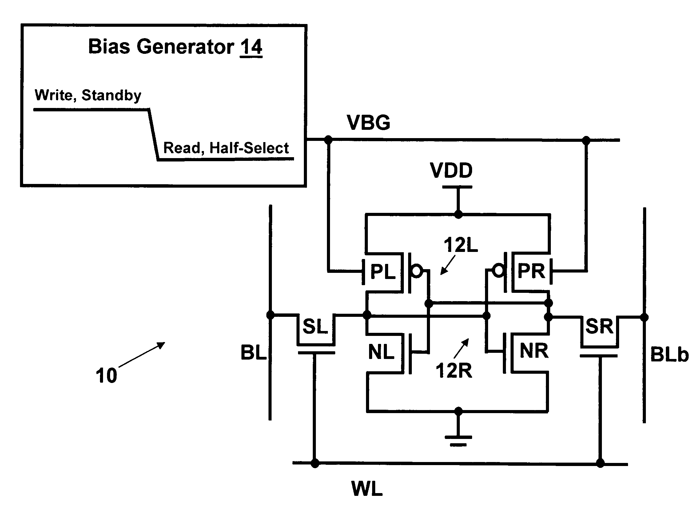
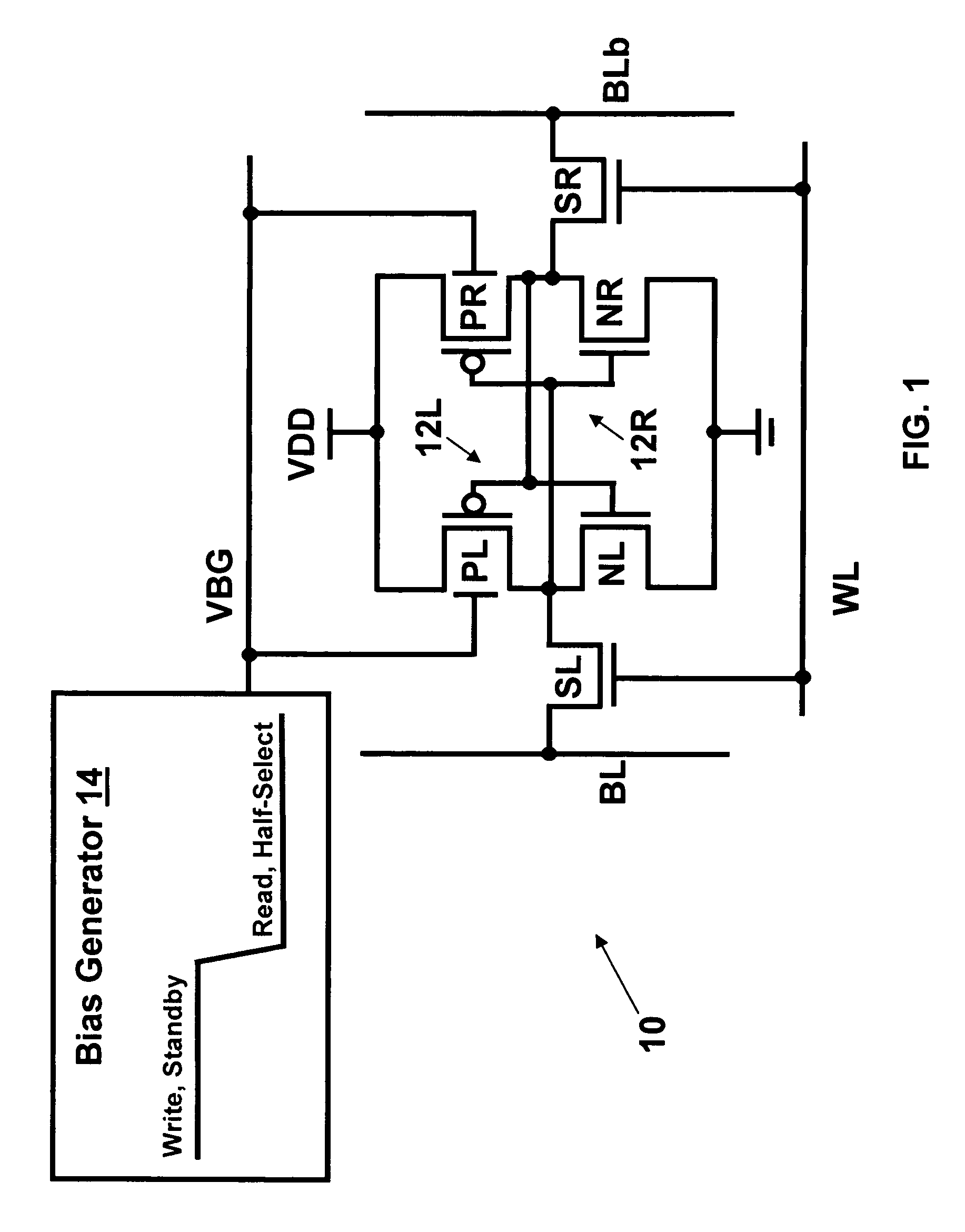
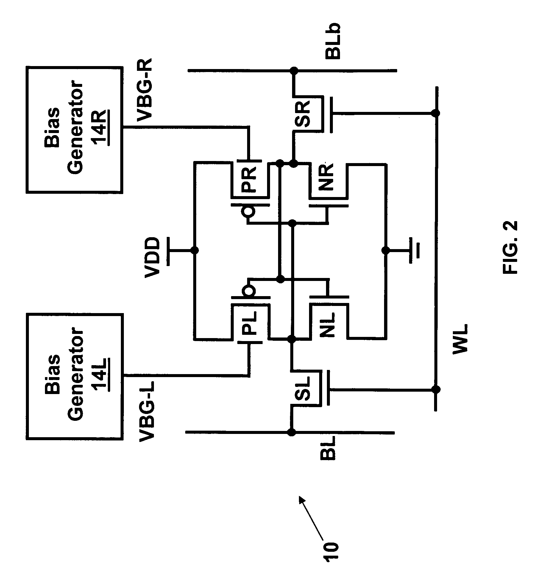
01 Independent gate bias control in forksheet transistors
Forksheet transistors can be designed with independent gate bias control mechanisms that allow separate voltage application to different gate structures. This enables precise control over transistor performance characteristics such as threshold voltage and drive current. The independent biasing capability is achieved through isolated gate electrodes and dedicated bias circuitry, allowing optimization of n-type and p-type devices independently within the forksheet architecture.- Gate bias control structures in forksheet transistors: Forksheet transistors utilize specialized gate bias control structures to manage the electrical characteristics of the device. These structures enable independent control of multiple gates, allowing for optimized threshold voltage adjustment and improved device performance. The gate bias control can be implemented through dedicated bias lines and contact structures that provide precise voltage control to the gate electrodes.
- Threshold voltage adjustment through body biasing: Body biasing techniques are employed in forksheet transistor architectures to dynamically adjust threshold voltages. This approach involves applying bias voltages to the substrate or body regions of the transistor, enabling fine-tuning of device characteristics for different operating modes. The body bias can be applied through isolated wells or dedicated bias contacts to achieve optimal performance across various operating conditions.
- Multi-gate bias configuration for performance optimization: Forksheet transistors incorporate multi-gate configurations where different bias voltages can be applied to separate gate structures. This enables independent control of different transistor regions, allowing for enhanced electrostatic control and reduced short-channel effects. The multi-gate bias approach provides flexibility in optimizing drive current, leakage current, and switching speed characteristics.
- Gate work function engineering for bias optimization: Gate work function engineering is utilized in forksheet transistors to optimize the built-in bias characteristics. Different gate materials or material combinations are selected to achieve desired threshold voltages without requiring excessive external bias. This approach involves using metal gates with specific work functions or multi-layer gate stacks to establish optimal electrostatic conditions.
- Bias voltage distribution networks for forksheet arrays: Specialized bias voltage distribution networks are designed to deliver appropriate gate bias voltages across arrays of forksheet transistors. These networks include routing structures, voltage regulators, and switching elements that ensure uniform and stable bias conditions throughout the integrated circuit. The distribution system minimizes voltage drops and provides isolation between different bias domains to maintain device performance consistency.
02 Back gate biasing techniques for forksheet structures
Back gate biasing methods are employed in forksheet transistor designs to modulate channel conductivity and control leakage currents. These techniques involve applying bias voltages to substrate or buried gate structures positioned beneath the active channel regions. Back gate bias can be used to dynamically adjust transistor characteristics during operation, providing additional degrees of freedom for performance optimization and power management.Expand Specific Solutions03 Gate work function engineering for threshold voltage control
Gate work function engineering is utilized in forksheet transistors to establish appropriate threshold voltages through material selection and gate stack design. Different metal gate materials with varying work functions are strategically positioned to achieve desired electrical characteristics. This approach enables precise threshold voltage targeting without relying solely on channel doping, which is particularly important in advanced forksheet architectures where dimensional scaling limits traditional doping techniques.Expand Specific Solutions04 Dynamic gate bias modulation for performance enhancement
Dynamic gate bias modulation techniques are implemented to adaptively adjust transistor performance based on operational requirements. These methods involve varying gate bias voltages in response to circuit conditions, workload demands, or power constraints. The dynamic biasing approach allows forksheet transistors to operate in different modes, balancing between high performance and low power consumption, and can be controlled through on-chip bias generation circuits or external control signals.Expand Specific Solutions05 Gate dielectric optimization for bias stability
Gate dielectric materials and structures are optimized in forksheet transistors to ensure stable operation under various bias conditions. High-k dielectric materials are employed to reduce gate leakage while maintaining adequate gate control. The dielectric stack design addresses bias temperature instability and charge trapping effects that can degrade transistor performance over time. Interface engineering between the gate dielectric and channel material is critical for achieving reliable bias characteristics and minimizing threshold voltage shifts.Expand Specific Solutions
Key Players in Advanced Semiconductor Manufacturing
The forksheet transistor gate bias optimization field represents an emerging segment within advanced semiconductor manufacturing, currently in the early development stage with significant growth potential. The market remains nascent as the industry transitions from FinFET to next-generation architectures, with forksheet technology positioned as a critical enabler for sub-3nm nodes. Technology maturity varies considerably among key players, with Samsung Electronics, TSMC, and Intel leading foundational research and early implementation. GlobalFoundries, IBM, and SMIC contribute specialized manufacturing expertise, while Qualcomm and Huawei drive application-specific requirements. The competitive landscape shows established semiconductor giants leveraging existing capabilities alongside emerging players like Innoscience focusing on specialized device optimization, creating a dynamic ecosystem where traditional foundries compete with integrated device manufacturers for technological leadership in this transformative transistor architecture.
Samsung Electronics Co., Ltd.
Technical Solution: Samsung has implemented a comprehensive gate bias optimization strategy for forksheet transistors that leverages their advanced 3nm process technology capabilities. Their approach utilizes multi-threshold voltage options through work function metal tuning, combined with optimized gate stack materials including high-k dielectrics with improved interface quality. Samsung's solution incorporates adaptive body biasing techniques specifically designed for the forksheet geometry, enabling dynamic threshold voltage adjustment for power and performance optimization. The company has developed proprietary gate contact schemes that minimize parasitic resistance while maintaining excellent electrostatic control over the channel region, particularly important for the thin silicon sheets in forksheet devices.
Strengths: Leading-edge manufacturing capabilities with high-volume production experience and strong R&D investment. Weaknesses: Intense competition in foundry market, complex manufacturing processes increase cost structure.
International Business Machines Corp.
Technical Solution: IBM has developed advanced gate bias optimization techniques for forksheet transistors through their comprehensive process-device co-optimization approach. Their methodology focuses on implementing dual work function metal gates with precise threshold voltage tuning capabilities, enabling independent control of NFET and PFET characteristics within the forksheet architecture. IBM's solution incorporates advanced gate stack engineering with high-k dielectrics and optimized interface treatments to minimize gate leakage while maintaining excellent electrostatic control. Their approach includes sophisticated bias schemes that leverage the unique geometry of forksheet devices to achieve superior short channel control and reduced variability compared to conventional FinFET structures.
Strengths: Pioneer in forksheet technology development with strong research foundation and advanced process capabilities. Weaknesses: Limited manufacturing scale compared to pure-play foundries, higher development costs.
Core Innovations in Forksheet Gate Control
Dynamic control of back gate bias in a FinFET SRAM cell
PatentInactiveUS7681628B2
Innovation
- Dynamic control of back gate bias voltage on pull-up pFETs in FinFET SRAM cells using a bias voltage generator that adjusts based on operational modes, optimizing threshold voltage and reducing leakage currents.

Bipolar transistor operating method with base charge controlled by back gate bias
PatentInactiveUS5627401A
Innovation
- A bipolar transistor with a silicon-on-insulator-on-silicon (SOIS) configuration and a back gate contact structure that applies a back gate bias voltage, reducing the sensitivity of the active base charge to collector-base bias by bypassing the sensitive portion of the base region, allowing independent control of the base charge and reducing base-collector resistance.


Manufacturing Process Integration Considerations
The manufacturing process integration for optimizing gate bias in forksheet transistors presents unique challenges that require careful coordination across multiple fabrication stages. The forksheet architecture demands precise control over the gate formation process, particularly in managing the dual-gate structure that defines the technology's core advantage. Critical integration points include the initial fin formation, where silicon nanosheets must be precisely patterned to enable subsequent gate wrapping, and the gate stack deposition, which requires uniform coverage around the complex three-dimensional geometry.
Thermal budget management becomes particularly crucial during gate bias optimization processes. The multiple annealing steps required for dopant activation and interface quality improvement must be carefully sequenced to prevent degradation of the delicate nanosheet structures. Integration teams must balance the thermal requirements for optimal gate bias characteristics against the structural integrity of the forksheet geometry, often requiring novel low-temperature processing techniques or rapid thermal annealing protocols.
The interconnect integration phase introduces additional complexity when implementing optimized gate bias schemes. Metal gate work function tuning, essential for achieving desired threshold voltages, must be coordinated with the overall backend-of-line processing flow. This includes managing stress effects from overlying dielectric layers and ensuring compatibility with standard via formation processes. The unique geometry of forksheet devices also necessitates modified chemical mechanical polishing procedures to achieve proper gate height uniformity.
Process monitoring and control systems require significant adaptation to accommodate forksheet-specific requirements. Traditional metrology techniques may prove inadequate for measuring critical dimensions within the complex gate structure, necessitating advanced characterization methods such as high-resolution transmission electron microscopy or specialized electrical test structures. Real-time process control algorithms must be developed to maintain consistent gate bias optimization across wafer-to-wafer and lot-to-lot variations.
Yield optimization strategies must address the increased process complexity inherent in forksheet manufacturing. Statistical process control methods need enhancement to account for the additional variables introduced by gate bias optimization procedures. Integration engineers must develop robust design rules that ensure manufacturability while preserving the performance benefits achieved through optimized gate biasing, requiring close collaboration between device design and process development teams.
Power Efficiency and Performance Trade-offs
The optimization of gate bias in forksheet transistors presents a fundamental trade-off between power efficiency and performance characteristics that significantly impacts device design decisions. This balance becomes increasingly critical as semiconductor manufacturers push toward advanced node technologies where power consumption and switching speed requirements must be carefully balanced to meet diverse application demands.
Power efficiency in forksheet transistors is primarily governed by the static and dynamic power consumption characteristics under varying gate bias conditions. Lower gate bias voltages typically reduce leakage currents, thereby minimizing static power dissipation during standby operations. However, this reduction in bias voltage directly impacts the transistor's drive current capability, leading to slower switching transitions and reduced overall performance metrics.
The performance aspect of this trade-off manifests through several key parameters including switching speed, drive current strength, and signal integrity. Higher gate bias voltages enhance the transistor's ability to deliver strong drive currents, enabling faster rise and fall times during switching operations. This improved performance comes at the cost of increased power consumption, both through higher leakage currents and elevated dynamic switching power due to faster transition rates.
Dynamic power considerations reveal additional complexity in the trade-off relationship. While optimized gate bias can reduce switching energy per transition, the relationship between bias voltage and capacitive charging currents creates non-linear power scaling effects. The forksheet architecture's unique gate coupling characteristics further complicate this relationship, as bias optimization must account for inter-gate interference and parasitic coupling effects.
Temperature dependencies introduce another dimension to the power-performance trade-off analysis. Gate bias optimization strategies that perform well at nominal operating conditions may exhibit degraded efficiency or performance characteristics under elevated temperature conditions. The temperature coefficient of threshold voltage in forksheet devices requires bias compensation schemes that maintain optimal trade-off balance across the full operating temperature range.
Process variation sensitivity adds practical constraints to theoretical optimization approaches. Manufacturing variations in gate work function, oxide thickness, and channel doping profiles create statistical distributions in optimal bias points across device populations. Robust optimization strategies must account for these variations while maintaining acceptable yield rates and performance consistency across production lots.
Unlock deeper insights with PatSnap Eureka Quick Research — get a full tech report to explore trends and direct your research. Try now!
Generate Your Research Report Instantly with AI Agent
Supercharge your innovation with PatSnap Eureka AI Agent Platform!