Photonic Tensor Cores vs E-Beam Processors: AI Flexibility Comparison
MAY 11, 202610 MIN READ
Generate Your Research Report Instantly with AI Agent
PatSnap Eureka helps you evaluate technical feasibility & market potential.
Photonic and E-Beam AI Processing Background and Goals
The evolution of artificial intelligence processing has reached a critical juncture where traditional electronic architectures face fundamental limitations in meeting the exponentially growing computational demands of modern AI workloads. As Moore's Law approaches its physical boundaries, the semiconductor industry has witnessed the emergence of revolutionary processing paradigms that transcend conventional silicon-based approaches. Two particularly promising technologies have emerged from this technological renaissance: photonic tensor cores and electron beam processors, each representing distinct philosophical approaches to overcoming the computational bottlenecks that constrain contemporary AI systems.
Photonic tensor cores represent a paradigm shift toward leveraging the unique properties of light for computational purposes. This technology harnesses the inherent parallelism of optical signals, enabling simultaneous processing of multiple data streams through wavelength division multiplexing and spatial light modulation techniques. The fundamental advantage lies in photons' ability to travel at the speed of light while generating minimal heat, addressing two critical limitations of electronic processors: latency and thermal management. Early developments in this field emerged from telecommunications infrastructure, where optical signal processing had already demonstrated superior bandwidth capabilities compared to electronic alternatives.
Electron beam processors, conversely, exploit the precise control and manipulation of electron beams to perform computational operations at the nanoscale level. This technology builds upon decades of advancement in electron microscopy and lithography systems, repurposing the sophisticated beam control mechanisms for general-purpose computing applications. The approach offers unprecedented precision in charge manipulation and enables three-dimensional processing architectures that transcend the planar limitations of traditional semiconductor fabrication.
The primary technological goal driving both innovations centers on achieving superior computational flexibility while maintaining energy efficiency and processing speed. Traditional AI accelerators, including graphics processing units and tensor processing units, excel in specific computational patterns but struggle with the diverse algorithmic requirements of emerging AI applications. The heterogeneous nature of modern machine learning workloads demands processing architectures capable of dynamically adapting to varying computational patterns, from dense matrix operations in deep neural networks to sparse graph computations in reinforcement learning algorithms.
Both photonic and electron beam approaches aim to address the memory wall problem that severely limits contemporary AI processing efficiency. Current architectures suffer from significant energy consumption and latency penalties when transferring data between processing units and memory hierarchies. Photonic systems target this challenge through in-memory optical computing, where data storage and processing occur within the same optical medium. Electron beam processors approach this problem through near-data processing architectures that minimize data movement by positioning computational elements in close proximity to memory structures.
The convergence of these technologies represents a fundamental shift toward application-specific processing architectures that can dynamically reconfigure their computational characteristics based on workload requirements, promising unprecedented flexibility in AI processing capabilities.
Market Demand for Flexible AI Computing Architectures
The global AI computing market is experiencing unprecedented demand for flexible architectures capable of handling diverse workloads across multiple domains. Traditional fixed-function accelerators, while efficient for specific tasks, increasingly struggle to meet the evolving requirements of modern AI applications that span computer vision, natural language processing, scientific computing, and emerging neural network architectures. This shift has created substantial market pressure for computing solutions that can dynamically adapt to varying computational patterns without sacrificing performance efficiency.
Enterprise customers are driving significant demand for AI systems that can seamlessly transition between training and inference workloads. Cloud service providers require architectures that can efficiently serve multiple tenants with diverse AI model requirements, from transformer-based language models to convolutional neural networks for image processing. The ability to reconfigure computational resources in real-time has become a critical differentiator in competitive cloud AI services markets.
Edge computing applications present another compelling demand driver for flexible AI architectures. Autonomous vehicles, robotics, and IoT devices require processors capable of handling multiple AI tasks simultaneously while maintaining strict power and latency constraints. These applications cannot afford dedicated chips for each AI function, necessitating highly adaptable computing platforms that can optimize resource allocation based on real-time operational demands.
The rapid evolution of AI algorithms further amplifies market demand for architectural flexibility. Research institutions and technology companies require computing platforms that can accommodate experimental neural network topologies and novel training methodologies without requiring complete hardware redesigns. This need has intensified as AI research accelerates and new paradigms emerge regularly.
Financial markets reflect this demand through increased investment in companies developing reconfigurable AI computing solutions. Venture capital and corporate investment have shifted toward startups and established companies offering programmable AI accelerators, optical computing platforms, and hybrid architectures that promise greater adaptability than traditional approaches.
Manufacturing sectors are increasingly adopting AI for quality control, predictive maintenance, and process optimization, requiring computing systems that can handle multiple AI workloads within single production environments. These industrial applications demand robust, flexible architectures capable of supporting diverse AI models while maintaining operational reliability and cost-effectiveness across extended deployment periods.
Current State of Photonic Tensor Cores vs E-Beam Processors
Photonic tensor cores represent an emerging paradigm in AI acceleration, leveraging optical computing principles to perform matrix operations at the speed of light. Current implementations primarily utilize silicon photonics platforms, where optical signals encode data and perform computations through interference patterns and wavelength division multiplexing. Leading research institutions and companies have demonstrated prototype systems capable of executing neural network inference with significantly reduced power consumption compared to traditional electronic processors.
The photonic approach faces substantial technical challenges in achieving practical deployment. Signal-to-noise ratio limitations, thermal stability requirements, and the complexity of optical-electronic conversion interfaces remain significant barriers. Current photonic tensor cores excel in specific linear algebra operations but struggle with the full spectrum of AI workloads, particularly those requiring frequent data movement and complex control flow operations.
E-beam processors, utilizing electron beam lithography principles for computation, represent a more experimental approach to AI acceleration. These systems manipulate electron beams to perform parallel computations, potentially offering massive parallelism for specific AI algorithms. Current research focuses on proof-of-concept demonstrations rather than commercial implementations, with most work concentrated in academic laboratories exploring fundamental computational capabilities.
The electron beam approach encounters formidable engineering challenges, including vacuum system requirements, beam stability control, and integration with conventional computing architectures. Power consumption and thermal management present additional obstacles, as maintaining the precise environmental conditions necessary for stable electron beam operation requires significant energy overhead.
Both technologies currently operate in early research phases, with photonic systems showing more advanced development toward practical applications. Photonic tensor cores have achieved limited commercial prototyping, while e-beam processors remain largely theoretical constructs. The manufacturing complexity and cost considerations for both approaches significantly exceed conventional semiconductor processes, limiting their near-term commercial viability.
Integration challenges persist for both technologies, particularly in interfacing with existing AI software frameworks and hardware ecosystems. Current implementations require specialized programming models and cannot seamlessly replace traditional GPU or TPU architectures without substantial system redesign.
Existing Photonic Tensor Core and E-Beam Processing Solutions
01 Photonic computing architectures for AI processing
Advanced photonic computing systems that utilize light-based processing elements to perform artificial intelligence computations. These architectures leverage optical components and photonic circuits to enable high-speed parallel processing capabilities for machine learning algorithms and neural network operations, providing enhanced computational efficiency compared to traditional electronic processors.- Photonic computing architectures for AI processing: Advanced photonic computing systems that utilize light-based processing elements to perform artificial intelligence computations. These architectures leverage optical components and photonic circuits to enable high-speed parallel processing capabilities for machine learning algorithms and neural network operations, providing enhanced computational efficiency compared to traditional electronic systems.
- Tensor processing units with optical integration: Specialized processing units designed for tensor operations that incorporate optical elements to enhance computational performance. These systems combine traditional tensor processing capabilities with photonic components to achieve improved throughput and energy efficiency for matrix operations commonly used in deep learning and artificial intelligence applications.
- Electron beam processing systems for flexible AI computation: Electron beam-based processing technologies that provide adaptable computational capabilities for artificial intelligence workloads. These systems utilize controlled electron beams to perform various computational tasks with high precision and flexibility, enabling dynamic reconfiguration of processing parameters to accommodate different AI algorithm requirements.
- Hybrid photonic-electronic processing architectures: Integrated systems that combine photonic and electronic processing elements to create flexible artificial intelligence computing platforms. These hybrid architectures leverage the advantages of both optical and electronic components to provide scalable and adaptable processing capabilities for diverse machine learning applications and neural network implementations.
- Reconfigurable optical computing systems for AI flexibility: Dynamically reconfigurable optical computing platforms designed to provide flexible artificial intelligence processing capabilities. These systems feature programmable optical components and adaptive architectures that can be modified in real-time to optimize performance for different computational tasks, enabling efficient execution of various machine learning algorithms and neural network topologies.
02 Tensor processing units with optical integration
Specialized processing units designed for tensor operations that incorporate optical elements to enhance computational performance. These systems combine traditional tensor processing capabilities with photonic components to accelerate matrix operations and multi-dimensional array computations commonly used in deep learning and artificial intelligence applications.Expand Specific Solutions03 Electron beam processing systems for flexible AI computation
Electron beam-based processing technologies that provide adaptable and reconfigurable computing capabilities for artificial intelligence workloads. These systems utilize controlled electron beams to perform computational operations with high precision and flexibility, enabling dynamic reconfiguration of processing elements to optimize performance for different AI algorithms and applications.Expand Specific Solutions04 Hybrid photonic-electronic tensor core architectures
Integrated computing systems that combine photonic and electronic components within tensor core architectures to achieve optimal performance for AI processing. These hybrid systems leverage the advantages of both optical and electronic processing methods, providing enhanced bandwidth, reduced latency, and improved energy efficiency for complex tensor operations and neural network computations.Expand Specific Solutions05 Adaptive processing frameworks for AI workload optimization
Flexible computing frameworks that dynamically adapt processing resources and architectures to optimize performance for varying artificial intelligence workloads. These systems incorporate reconfigurable processing elements, adaptive scheduling algorithms, and intelligent resource allocation mechanisms to maximize computational efficiency across different types of AI applications and algorithms.Expand Specific Solutions
Key Players in Photonic and E-Beam AI Processor Industry
The photonic tensor cores versus e-beam processors landscape represents an emerging AI acceleration market in early development stages, with significant growth potential driven by increasing demand for energy-efficient, high-performance computing solutions. The market remains nascent with limited commercial deployment, though projected to expand rapidly as AI workloads intensify. Technology maturity varies considerably across players: established giants like IBM and Meta Platforms leverage substantial R&D resources for photonic computing research, while specialized startups including Lightmatter, CogniFiber, and Kepler Computing focus on breakthrough photonic architectures. Chinese companies such as Shanghai Biren Technology and Shanghai Iluvatar CoreX are developing competitive AI chip solutions, supported by academic institutions like MIT, Harvard, and Huazhong University of Science & Technology advancing fundamental research in optical computing and neuromorphic architectures for next-generation AI processing systems.
International Business Machines Corp.
Technical Solution: IBM has developed advanced photonic computing architectures integrated with their neuromorphic computing research. Their approach combines silicon photonics with electronic control systems to create hybrid tensor processing units. IBM's photonic tensor cores utilize coherent optical computing principles, employing Mach-Zehnder interferometers and microring resonators for matrix multiplication operations. The system provides flexibility through software-defined optical routing and supports various AI model architectures including convolutional neural networks and transformer models through adaptive wavelength management and optical switching capabilities.
Strengths: Mature silicon photonics technology, strong research foundation, hybrid electronic-photonic integration. Weaknesses: Complex manufacturing requirements, higher development costs, limited commercial availability.
Lightmatter, Inc.
Technical Solution: Lightmatter develops photonic tensor processing units that utilize light-based computing for AI workloads. Their Passage interconnect technology enables high-bandwidth, low-latency communication between processors using photonic links. The company's photonic tensor cores leverage wavelength division multiplexing to perform matrix operations at the speed of light, offering significant advantages in power efficiency and computational throughput for neural network inference and training. Their architecture supports flexible AI workloads by dynamically reconfiguring optical pathways and wavelength assignments to optimize for different neural network topologies and computational requirements.
Strengths: Ultra-low latency photonic processing, exceptional power efficiency, high bandwidth interconnects. Weaknesses: Limited programmability compared to electronic processors, sensitivity to environmental conditions.
Core Innovations in Photonic vs E-Beam AI Flexibility
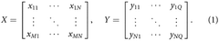
Photonic tensor core devices and systems
PatentWO2025096551A1
Innovation
- The development of photonic tensor core devices that utilize sets of optical modulators for encoding matrix values onto optical signals, combined with dot product engines for combining these signals and generating product photocurrent signals, which are then converted to digital electric signals. This design includes slow-light Mach-Zehnder modulators for enhanced light-matter interaction, reducing size and power consumption while maintaining thermal robustness.
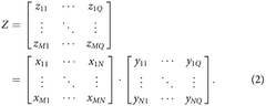

Photonic tensor core matrix vector multiplier
PatentPendingUS20230152667A1
Innovation
- A photonic tensor core processor system that performs optical and electro-optical tensor operations using modular sub-modules with photonic dot product engines, enabling parallel and efficient multiply-accumulate operations through integrated photonics and fiber optics, allowing for matrix-matrix, matrix-vector, and vector-matrix multiplications.


Energy Efficiency Standards for Next-Gen AI Processors
The emergence of next-generation AI processors, particularly photonic tensor cores and electron-beam processors, necessitates the establishment of comprehensive energy efficiency standards to guide industry development and ensure sustainable computing solutions. Current energy efficiency metrics for traditional silicon-based processors are inadequate for evaluating these novel architectures due to their fundamentally different operational principles and energy consumption patterns.
Photonic tensor cores operate through optical signal processing, utilizing photons rather than electrons for computation. This paradigm shift requires new energy efficiency standards that account for optical power consumption, laser efficiency, and electro-optical conversion losses. The primary energy consumption sources include laser diodes, optical modulators, and photodetectors, which exhibit different scaling behaviors compared to conventional CMOS transistors. Standards must address the unique challenge of measuring optical power efficiency while considering the wavelength-dependent losses in photonic circuits.
Electron-beam processors present distinct energy efficiency considerations, primarily related to beam generation, focusing systems, and substrate interaction mechanisms. The energy standards for these systems must encompass beam current efficiency, acceleration voltage optimization, and thermal management requirements. Unlike photonic systems, e-beam processors face significant challenges in power scaling due to space-charge effects and beam-substrate interaction dynamics that directly impact computational throughput per watt.
Establishing unified energy efficiency standards requires defining new metrics beyond traditional operations-per-joule measurements. For photonic systems, standards should incorporate optical insertion loss, modulation efficiency, and wavelength division multiplexing capabilities. E-beam processors require metrics addressing beam utilization efficiency, parallel processing capabilities, and substrate-specific energy requirements for different computational tasks.
The standardization framework must also consider the hybrid nature of these processors, where conventional electronic circuits interface with photonic or electron-beam components. Energy efficiency standards should account for the overhead associated with signal conversion between different physical domains and the power requirements of supporting electronic systems such as drivers, amplifiers, and control circuits.
Thermal management represents another critical aspect requiring standardized evaluation methods. Photonic processors generate heat through optical absorption and electrical driving circuits, while e-beam systems face challenges related to beam-induced heating and high-voltage power supply efficiency. Standards must define thermal efficiency metrics that correlate with computational performance and long-term reliability.
Future energy efficiency standards should incorporate dynamic power management capabilities, enabling adaptive operation modes based on computational workload requirements. This includes defining standards for power gating, frequency scaling, and workload-dependent optimization strategies specific to photonic and electron-beam architectures, ensuring these next-generation processors can meet diverse AI application demands while maintaining optimal energy performance.
Scalability Challenges in Advanced AI Computing Architectures
The scalability challenges facing advanced AI computing architectures, particularly photonic tensor cores and electron-beam processors, represent fundamental limitations that could constrain the future development of artificial intelligence systems. These challenges emerge from the intersection of physical constraints, architectural design decisions, and the exponential growth in computational demands driven by increasingly complex AI models.
Photonic tensor cores encounter significant scalability bottlenecks primarily related to optical component integration density and thermal management. As the number of photonic processing elements increases, maintaining coherent light propagation across larger chip areas becomes increasingly difficult due to phase noise accumulation and optical loss. The wavelength division multiplexing approach, while enabling parallel processing, faces fundamental limits imposed by the available optical spectrum and crosstalk between adjacent channels. Additionally, the hybrid nature of photonic-electronic interfaces creates bandwidth bottlenecks that become more pronounced as system scale increases.
Electron-beam processors face distinct scalability challenges rooted in their sequential processing nature and beam management complexity. The fundamental limitation stems from space-charge effects that occur when multiple electron beams operate in proximity, leading to beam deflection and reduced processing accuracy. As the number of parallel electron beams increases to improve throughput, electromagnetic interference between beams becomes a critical constraint. The vacuum requirements for electron-beam operation also present scalability challenges, as maintaining ultra-high vacuum conditions across larger processing volumes requires exponentially increasing pumping capacity and more sophisticated chamber designs.
Power consumption scaling represents a critical challenge for both architectures. Photonic systems require high-power laser sources and temperature-controlled environments to maintain operational stability, with power requirements scaling non-linearly with system size. Electron-beam processors demand substantial power for beam generation, focusing systems, and vacuum maintenance, creating thermal management challenges that compound with increased scale.
Manufacturing complexity introduces additional scalability constraints. Photonic tensor cores require precise alignment of optical components with tolerances measured in nanometers, making large-scale integration increasingly difficult and expensive. Electron-beam processors face similar precision requirements for beam focusing and deflection systems, with manufacturing costs rising exponentially as the number of parallel processing elements increases.
The interconnect challenge becomes particularly acute in scaled implementations. Both architectures struggle with efficient data movement between processing elements and external memory systems, creating potential bottlenecks that limit overall system performance regardless of individual processor capabilities.
Unlock deeper insights with PatSnap Eureka Quick Research — get a full tech report to explore trends and direct your research. Try now!
Generate Your Research Report Instantly with AI Agent
Supercharge your innovation with PatSnap Eureka AI Agent Platform!