

Plasma Dicing vs Laser Scribe+Break: Which Boosts Throughput
MAY 9, 20269 MIN READ
Generate Your Research Report Instantly with AI Agent
PatSnap Eureka helps you evaluate technical feasibility & market potential.
Plasma Dicing and Laser Scribe Evolution Background
Semiconductor wafer dicing technology has undergone significant evolution since the early days of integrated circuit manufacturing. Traditional mechanical sawing dominated the industry for decades, utilizing diamond-embedded blades to physically cut through silicon wafers. While effective for larger die sizes, mechanical dicing faced inherent limitations including kerf loss, chipping, and contamination issues that became increasingly problematic as device dimensions continued to shrink.
The emergence of laser-based dicing technologies in the 1990s marked a pivotal shift in wafer processing capabilities. Initial laser dicing systems employed direct ablation methods, where high-energy laser pulses vaporized material along predetermined cutting paths. However, these early systems struggled with heat-affected zones and debris generation, limiting their adoption in high-precision applications.
The development of laser scribe-and-break methodology represented a significant advancement in addressing throughput challenges. This approach involves creating controlled stress concentration points through precise laser scribing, followed by mechanical breaking along the weakened lines. The technique offered improved processing speeds compared to full-cut laser dicing while maintaining acceptable edge quality for many applications.
Plasma dicing technology emerged as a revolutionary alternative in the early 2000s, fundamentally changing the paradigm of wafer singulation. Unlike traditional methods that process wafers from the front side, plasma dicing employs a unique approach where wafers are temporarily bonded to carrier substrates, ground to expose streets, and then subjected to plasma etching processes. This method eliminates mechanical stress and enables processing of ultra-thin wafers that would be impossible to handle with conventional techniques.
The evolution toward plasma dicing was driven by the semiconductor industry's relentless pursuit of higher device density and thinner form factors. As mobile devices demanded increasingly compact components, traditional dicing methods reached their physical limitations. Plasma dicing addressed these challenges by enabling the processing of wafers as thin as 25 micrometers while maintaining excellent die strength and edge quality.
Both plasma dicing and laser scribe-and-break technologies continue to evolve, with recent developments focusing on throughput optimization, process automation, and integration with advanced packaging technologies. The choice between these methods increasingly depends on specific application requirements, including die thickness, material properties, and production volume considerations.
Market Demand for High-Throughput Wafer Dicing Solutions
The semiconductor industry faces unprecedented pressure to increase wafer processing throughput while maintaining precision and yield quality. As device miniaturization continues and production volumes escalate, manufacturers require dicing solutions that can handle increasingly complex substrates including ultra-thin wafers, advanced packaging materials, and compound semiconductors. Traditional mechanical dicing methods struggle to meet these evolving requirements, creating substantial market demand for advanced dicing technologies.
Market drivers primarily stem from the explosive growth in consumer electronics, automotive semiconductors, and emerging applications such as 5G infrastructure and artificial intelligence chips. These sectors demand higher production volumes with shorter cycle times, pushing manufacturers to seek dicing solutions that can significantly reduce processing time per wafer while maintaining edge quality standards. The transition toward smaller die sizes and thinner substrates further intensifies the need for precision dicing methods that minimize mechanical stress and chipping.
The competitive landscape reveals strong demand for solutions that can process diverse substrate materials efficiently. Silicon carbide, gallium nitride, and other wide-bandgap semiconductors present unique challenges that conventional dicing approaches cannot adequately address. Manufacturers increasingly prioritize dicing technologies that offer versatility across multiple material types without compromising throughput performance.
Cost optimization remains a critical market driver, as semiconductor manufacturers seek to reduce overall manufacturing expenses while scaling production capacity. High-throughput dicing solutions directly impact the total cost of ownership by reducing processing time, minimizing material waste, and improving overall equipment effectiveness. The ability to process more wafers per hour translates directly into improved profitability and competitive positioning.
Quality requirements continue to escalate as device performance specifications become more stringent. Market demand focuses on dicing solutions that can achieve superior edge quality, minimal heat-affected zones, and reduced subsurface damage while maintaining high processing speeds. This dual requirement for speed and precision creates opportunities for advanced technologies that can deliver both attributes simultaneously.
The market also demonstrates growing interest in flexible manufacturing solutions that can adapt to varying production requirements. Manufacturers seek dicing technologies that can efficiently handle both high-volume production runs and smaller specialty batches without significant setup time or performance degradation, reflecting the industry's move toward more agile manufacturing approaches.
Current State of Plasma vs Laser Dicing Technologies
Plasma dicing technology has emerged as a revolutionary approach to semiconductor wafer singulation, utilizing reactive ion etching processes to achieve precise cuts without mechanical stress. Current plasma dicing systems employ fluorine-based chemistries, typically SF6 or CF4, combined with oxygen to create anisotropic etching profiles. Leading equipment manufacturers like SPTS Technologies and Panasonic have developed advanced plasma dicing platforms capable of processing wafers up to 300mm diameter with edge quality superior to traditional methods.
The technology operates through a mask-based process where photoresist patterns define the dicing streets, followed by deep reactive ion etching to create trenches with near-vertical sidewalls. Modern plasma dicing systems achieve etch rates of 3-5 μm/min with aspect ratios exceeding 20:1, enabling processing of ultra-thin wafers down to 25 μm thickness without chipping or cracking.
Laser scribe and break technology represents the established approach, utilizing focused laser beams to create controlled fracture initiation points followed by mechanical breaking. Current laser systems predominantly employ green lasers (532nm) and UV lasers (355nm) for scribing, with recent advances incorporating picosecond and femtosecond pulse durations to minimize heat-affected zones. Market leaders including Disco Corporation and Advanced Dicing Technologies have developed high-speed laser scribing systems achieving processing speeds up to 1000 mm/s.
The laser scribe process creates micro-cracks along predetermined lines, typically 10-30% of wafer thickness, followed by controlled mechanical stress application to propagate fractures. Modern systems integrate real-time monitoring and adaptive power control to maintain consistent scribe quality across varying material properties and thicknesses.
Both technologies face distinct technical challenges in current implementations. Plasma dicing encounters limitations in throughput due to sequential processing requirements and chamber cycling times, while laser scribe and break systems struggle with edge quality consistency on advanced packaging substrates. Recent developments focus on hybrid approaches combining plasma pre-treatment with laser finishing to optimize both speed and quality parameters.
Current market adoption shows plasma dicing gaining traction in high-value applications requiring superior edge quality, while laser scribe and break maintains dominance in high-volume production environments where throughput optimization remains the primary consideration for manufacturing economics.
Existing Plasma and Laser Dicing Solutions
01 Plasma dicing process optimization and control methods
Advanced plasma dicing techniques focus on optimizing process parameters such as gas flow rates, pressure conditions, and power settings to achieve higher throughput while maintaining precision. These methods involve sophisticated control systems that monitor and adjust plasma conditions in real-time to ensure consistent dicing quality and maximize processing speed.- Plasma dicing process optimization and control methods: Advanced plasma dicing techniques focus on optimizing process parameters such as plasma power, gas flow rates, and chamber pressure to achieve higher throughput while maintaining precision. These methods involve real-time monitoring and feedback control systems to ensure consistent dicing quality and reduce processing time. The optimization includes plasma source configuration and substrate handling mechanisms to maximize efficiency.
- Laser scribing and breaking mechanisms for semiconductor processing: Laser scribe and break technology utilizes precise laser beam control to create controlled fracture lines in semiconductor wafers. The process involves optimized laser parameters including wavelength, pulse duration, and beam focusing to achieve clean breaks with minimal material loss. Advanced beam delivery systems and substrate positioning mechanisms enhance the accuracy and speed of the scribing process.
- Throughput enhancement through automated handling and positioning systems: High-throughput processing is achieved through sophisticated wafer handling and positioning systems that minimize setup time and maximize processing efficiency. These systems incorporate robotic handling, precision alignment mechanisms, and multi-wafer processing capabilities. Advanced scheduling algorithms and parallel processing techniques further optimize the overall system throughput.
- Integrated plasma and laser processing systems: Combined processing systems integrate both plasma dicing and laser scribing capabilities in a single platform to optimize workflow and reduce handling time. These systems feature coordinated process control, shared substrate handling mechanisms, and optimized chamber designs that allow for sequential or simultaneous processing operations. The integration reduces overall processing time and improves yield.
- Quality control and defect reduction in high-speed dicing operations: Advanced quality control systems monitor processing parameters in real-time to detect and prevent defects during high-speed dicing operations. These systems employ optical inspection, process monitoring sensors, and predictive algorithms to maintain consistent quality while maximizing throughput. Defect reduction techniques include optimized cutting strategies and environmental control systems.
02 Laser scribing and breaking mechanisms for semiconductor processing
Laser scribe and break processes utilize precise laser beam control to create controlled fracture lines in semiconductor materials. The technology involves optimized laser parameters including wavelength, pulse duration, and beam focusing to achieve clean breaks with minimal material loss and maximum throughput efficiency.Expand Specific Solutions03 Throughput enhancement through automated handling and positioning systems
Automated wafer handling and positioning systems are integrated with dicing processes to minimize cycle times and maximize throughput. These systems include robotic transfer mechanisms, precision alignment tools, and multi-stage processing capabilities that enable continuous operation with reduced manual intervention.Expand Specific Solutions04 Hybrid processing techniques combining plasma and laser methods
Integrated processing approaches combine plasma dicing with laser scribing techniques to leverage the advantages of both methods. These hybrid systems optimize the sequence and parameters of each process step to achieve superior throughput while maintaining high quality standards for semiconductor device separation.Expand Specific Solutions05 Quality control and monitoring systems for high-throughput dicing
Advanced monitoring and quality control systems are implemented to ensure consistent output quality during high-throughput dicing operations. These systems utilize real-time inspection technologies, feedback control mechanisms, and predictive maintenance algorithms to maintain optimal performance while maximizing processing speed.Expand Specific Solutions
Major Players in Dicing Equipment Manufacturing
The plasma dicing versus laser scribe+break competition represents a mature semiconductor processing market experiencing steady growth driven by increasing demand for miniaturized electronic devices. The market demonstrates significant scale with established players like Applied Materials, Intel, and DISCO Corp leading traditional approaches, while companies such as Hymson Laser Technology, Nanjing Multi-D Systems, and SILTECTRA drive innovation in plasma-based solutions. Technology maturity varies considerably across the competitive landscape - conventional laser scribing represents well-established technology with proven reliability, whereas plasma dicing emerges as an advanced alternative offering superior precision and reduced mechanical stress. Key differentiators include throughput capabilities, edge quality, and process flexibility, with plasma solutions generally commanding premium positioning despite higher initial investment costs, indicating an industry transition toward next-generation processing methodologies.
Electro Scientific Industries, Inc.
Technical Solution: ESI specializes in laser-based dicing solutions that compete directly with plasma dicing in terms of throughput and quality. Their advanced laser scribe and break systems utilize green wavelength lasers (532nm) combined with optimized beam shaping to create precise scribe lines with minimal heat-affected zones. The systems achieve cutting speeds up to 1000mm/s with positional accuracy within ±1μm, enabling high-throughput processing of various semiconductor materials including silicon, gallium arsenide, and silicon carbide. ESI's technology incorporates real-time process monitoring and adaptive control systems that automatically adjust laser parameters based on material properties and thickness variations, ensuring consistent quality across production runs.
Strengths: High cutting speeds, excellent precision, versatile material compatibility, real-time process control. Weaknesses: Potential for thermal damage, limited kerf width reduction, requires precise breaking control.
Applied Materials, Inc.
Technical Solution: Applied Materials offers comprehensive dicing solutions including both plasma dicing and laser-based systems for semiconductor manufacturing. Their plasma dicing technology employs advanced chamber designs with precise gas flow control and RF power management to achieve uniform etching across large wafer surfaces. The system can process 300mm wafers with throughput rates exceeding 200 wafers per hour, significantly outperforming traditional laser scribe and break methods. Their laser dicing systems utilize ultrafast picosecond lasers for stealth dicing applications, creating subsurface modifications that enable clean breaking with minimal thermal damage. The integrated approach allows manufacturers to choose optimal dicing methods based on specific device requirements and production volumes.
Strengths: Comprehensive solution portfolio, high-volume production capability, excellent process control. Weaknesses: Complex system integration, high maintenance requirements, significant capital investment needed.
Core Patents in Advanced Dicing Technologies
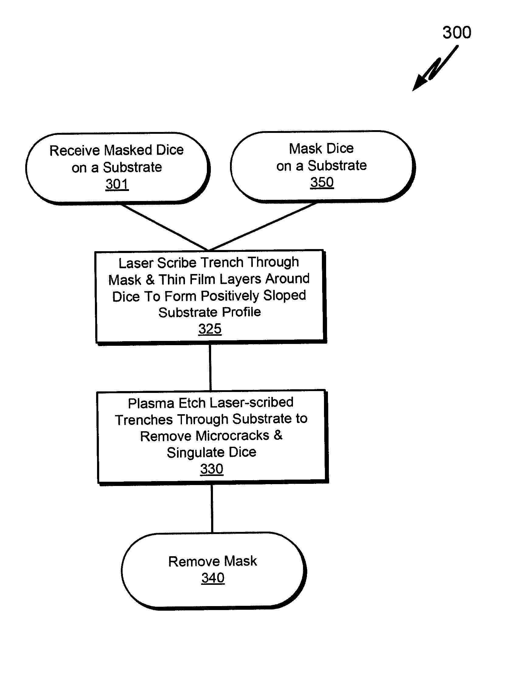
Maskless hybrid laser scribing and plasma etching wafer dicing process
PatentWO2015060968A1
Innovation
- A maskless hybrid laser scribing and plasma etching process is employed, where a femtosecond-based laser scribes through a thick passivation layer to expose the wafer, followed by plasma etching to singulate the circuits, with the passivation layer protecting the integrated circuits and being thinned post-processing to access metal bumps, eliminating the need for additional mask coatings and reducing damage.


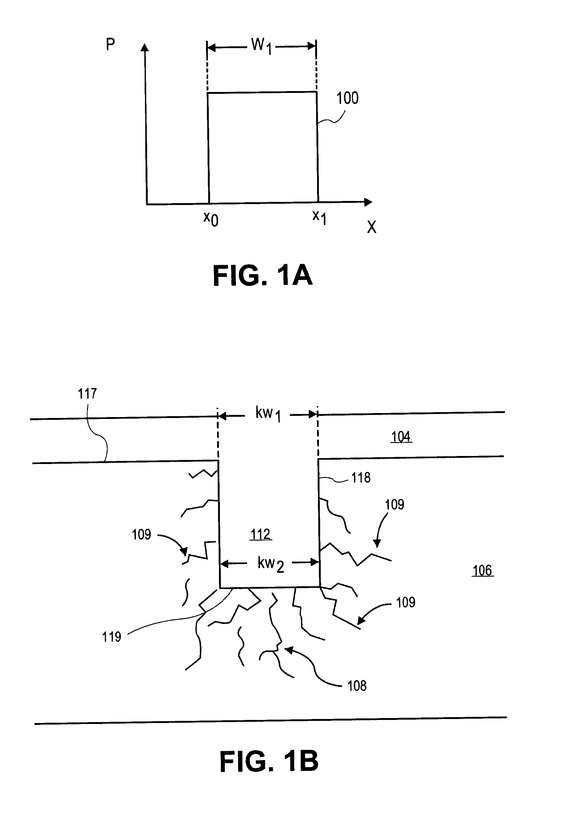
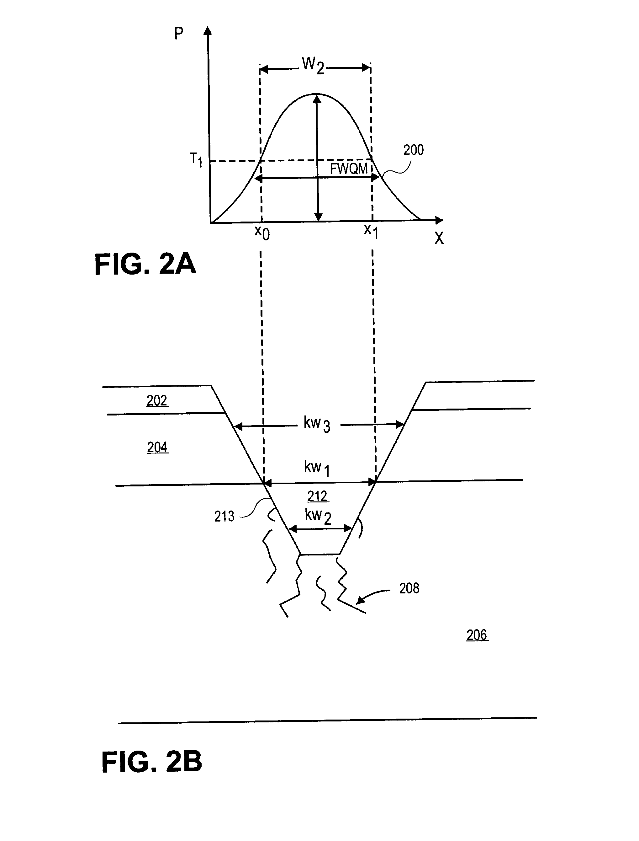
Damage isolation by shaped beam delivery in laser scribing process
PatentActiveUS20150217401A1
Innovation
- The method employs a laser scribing process using a centrally peaked spatial power profile to form sloped ablated sidewalls, followed by an anisotropic deep trench etch process to singulate ICs, which reduces microcrack formation and integrates a hybrid laser scribing and plasma etching system for efficient dicing.

Equipment Cost and ROI Analysis
The initial capital expenditure for plasma dicing systems typically ranges from $2.5 million to $4.5 million per unit, significantly higher than laser scribe+break systems which cost between $800,000 to $1.5 million. This substantial difference stems from plasma dicing's complex chamber design, advanced gas delivery systems, and sophisticated process control requirements. However, the equipment cost analysis must consider the total cost of ownership rather than just initial investment.
Operational expenses reveal a more nuanced picture. Plasma dicing systems consume approximately 15-25% more electricity due to RF power requirements and vacuum pumping systems. Gas consumption costs add $0.02-0.05 per wafer processed, while laser systems primarily incur costs from periodic laser tube replacements averaging $50,000-80,000 annually. Maintenance complexity differs significantly, with plasma systems requiring specialized technicians and more frequent chamber cleaning cycles.
Throughput capabilities directly impact ROI calculations. Plasma dicing achieves 200-400 wafers per hour depending on die size and complexity, while laser scribe+break typically processes 150-250 wafers per hour. The 30-60% throughput advantage of plasma dicing becomes crucial in high-volume manufacturing environments where equipment utilization rates exceed 80%.
ROI analysis over a five-year period shows plasma dicing achieving break-even at production volumes exceeding 50,000 wafers annually. Below this threshold, laser scribe+break demonstrates superior financial performance due to lower capital requirements. The crossover point varies based on die complexity, with smaller die sizes favoring plasma dicing due to reduced kerf loss and improved yield rates.
Depreciation schedules significantly influence ROI calculations. Plasma dicing equipment typically depreciates over 7-10 years compared to 5-7 years for laser systems, affecting tax implications and replacement planning. Additionally, plasma systems maintain higher resale values, retaining 25-35% of original cost after five years versus 15-25% for laser equipment.
The total economic impact includes indirect benefits such as reduced downstream processing costs and improved product quality metrics. Plasma dicing eliminates mechanical stress-related defects, potentially reducing field failure rates by 15-20%, translating to significant warranty cost savings and enhanced customer satisfaction in high-reliability applications.
Process Quality and Yield Optimization Strategies
Process quality and yield optimization strategies for semiconductor dicing operations require comprehensive approaches that address both technological capabilities and operational efficiency. The choice between plasma dicing and laser scribe+break methodologies significantly impacts overall manufacturing performance, necessitating careful evaluation of quality control parameters and yield enhancement techniques.
Quality optimization in plasma dicing centers on precise control of plasma parameters including gas flow rates, RF power density, and chamber pressure. Advanced process monitoring systems enable real-time adjustment of these variables to maintain consistent etch rates and minimize die edge chipping. Temperature management during plasma processing prevents thermal stress-induced defects, while endpoint detection algorithms ensure uniform die separation across wafer surfaces.
Laser scribe+break processes demand different optimization strategies focused on laser power modulation and mechanical breaking force calibration. Beam positioning accuracy and pulse duration control directly influence scribe line quality, affecting subsequent breaking success rates. Adaptive laser power systems compensate for material variations across wafer thickness, reducing the occurrence of incomplete scribes or excessive heat-affected zones.
Yield enhancement strategies encompass predictive maintenance protocols for both dicing technologies. Statistical process control implementation tracks key performance indicators including die strength measurements, edge quality assessments, and contamination levels. Machine learning algorithms analyze historical process data to identify optimal parameter windows that maximize yield while maintaining throughput targets.
Defect reduction methodologies vary between technologies but share common principles of contamination control and mechanical precision. Plasma dicing benefits from chamber cleaning protocols and gas purity management, while laser systems require optical component maintenance and beam quality monitoring. Both processes utilize advanced inspection systems for real-time defect detection and process adjustment.
Integration of quality feedback loops enables continuous process improvement through automated parameter optimization. Wafer-level quality mapping identifies spatial variations in dicing performance, allowing for localized process adjustments. Yield prediction models incorporate multiple process variables to forecast manufacturing outcomes and guide preventive interventions before quality degradation occurs.
Unlock deeper insights with PatSnap Eureka Quick Research — get a full tech report to explore trends and direct your research. Try now!
Generate Your Research Report Instantly with AI Agent
Supercharge your innovation with PatSnap Eureka AI Agent Platform!