

Quantify Wafer Bond Adhesion Uniformity Using Scanning Acoustic Microscopy
MAY 20, 20269 MIN READ
Generate Your Research Report Instantly with AI Agent
PatSnap Eureka helps you evaluate technical feasibility & market potential.
Wafer Bonding Technology Background and SAM Integration Goals
Wafer bonding technology has emerged as a fundamental enablement for advanced semiconductor manufacturing, particularly in three-dimensional integration, MEMS fabrication, and heterogeneous device assembly. This critical process involves permanently joining two or more wafer surfaces through various mechanisms including direct bonding, anodic bonding, eutectic bonding, and adhesive bonding. The evolution of wafer bonding began in the 1980s with silicon-on-insulator applications and has progressively advanced to support complex multi-layer architectures in modern electronic systems.
The semiconductor industry's relentless pursuit of higher performance and miniaturization has driven wafer bonding from a niche manufacturing technique to an essential process technology. Early implementations focused primarily on achieving basic adhesion between surfaces, but contemporary applications demand precise control over bond uniformity, interface quality, and mechanical integrity across entire wafer surfaces. This evolution reflects the industry's transition from simple planar devices to sophisticated three-dimensional structures requiring multiple bonded interfaces.
Current market demands for wafer bonding technology are intensifying due to several converging factors. The proliferation of advanced packaging solutions, including through-silicon vias and chip stacking architectures, requires exceptional bond quality and uniformity. Additionally, emerging applications in photonics integration, power electronics, and quantum computing impose stringent requirements on interface characteristics that directly impact device performance and reliability.
Traditional quality assessment methods for wafer bonding have relied primarily on destructive testing techniques, cross-sectional analysis, and limited sampling approaches. These conventional methods provide insufficient spatial resolution and statistical confidence for modern manufacturing requirements. The inability to comprehensively evaluate bond uniformity across entire wafer surfaces represents a significant gap in process control and quality assurance capabilities.
Scanning Acoustic Microscopy represents a transformative approach to addressing these limitations by enabling non-destructive, high-resolution characterization of bonded interfaces. The integration of SAM technology with wafer bonding processes aims to establish quantitative metrics for adhesion uniformity, detect subsurface defects, and provide real-time feedback for process optimization. This technological convergence addresses the critical need for comprehensive quality assessment while maintaining manufacturing throughput and cost effectiveness.
The primary objectives of integrating SAM with wafer bonding technology encompass developing standardized measurement protocols, establishing correlation between acoustic signatures and mechanical properties, and implementing automated inspection systems capable of full-wafer analysis. These goals collectively aim to transform wafer bonding from an art-based process to a scientifically controlled manufacturing technology with predictable and reproducible outcomes.
The semiconductor industry's relentless pursuit of higher performance and miniaturization has driven wafer bonding from a niche manufacturing technique to an essential process technology. Early implementations focused primarily on achieving basic adhesion between surfaces, but contemporary applications demand precise control over bond uniformity, interface quality, and mechanical integrity across entire wafer surfaces. This evolution reflects the industry's transition from simple planar devices to sophisticated three-dimensional structures requiring multiple bonded interfaces.
Current market demands for wafer bonding technology are intensifying due to several converging factors. The proliferation of advanced packaging solutions, including through-silicon vias and chip stacking architectures, requires exceptional bond quality and uniformity. Additionally, emerging applications in photonics integration, power electronics, and quantum computing impose stringent requirements on interface characteristics that directly impact device performance and reliability.
Traditional quality assessment methods for wafer bonding have relied primarily on destructive testing techniques, cross-sectional analysis, and limited sampling approaches. These conventional methods provide insufficient spatial resolution and statistical confidence for modern manufacturing requirements. The inability to comprehensively evaluate bond uniformity across entire wafer surfaces represents a significant gap in process control and quality assurance capabilities.
Scanning Acoustic Microscopy represents a transformative approach to addressing these limitations by enabling non-destructive, high-resolution characterization of bonded interfaces. The integration of SAM technology with wafer bonding processes aims to establish quantitative metrics for adhesion uniformity, detect subsurface defects, and provide real-time feedback for process optimization. This technological convergence addresses the critical need for comprehensive quality assessment while maintaining manufacturing throughput and cost effectiveness.
The primary objectives of integrating SAM with wafer bonding technology encompass developing standardized measurement protocols, establishing correlation between acoustic signatures and mechanical properties, and implementing automated inspection systems capable of full-wafer analysis. These goals collectively aim to transform wafer bonding from an art-based process to a scientifically controlled manufacturing technology with predictable and reproducible outcomes.
Market Demand for Advanced Wafer Bond Quality Assessment
The semiconductor industry's relentless pursuit of miniaturization and performance enhancement has created unprecedented demands for advanced wafer bonding technologies. As device architectures become increasingly complex with three-dimensional integration, through-silicon vias, and heterogeneous material combinations, the quality requirements for wafer-to-wafer bonds have intensified dramatically. Traditional bonding quality assessment methods are proving inadequate for next-generation applications where even microscopic defects can compromise device functionality and yield.
Market drivers for advanced wafer bond quality assessment stem from multiple high-growth sectors. The memory semiconductor market, particularly in NAND flash and DRAM manufacturing, requires exceptional bond uniformity to ensure reliable data storage and retrieval across stacked memory layers. Power semiconductor applications demand robust bonding to handle thermal cycling and mechanical stress, while MEMS devices require precise bond characterization to maintain sensor accuracy and mechanical integrity.
The automotive electronics sector presents particularly stringent requirements as vehicles transition toward autonomous driving and electrification. Safety-critical applications cannot tolerate bond failures that might occur due to temperature fluctuations, vibration, or long-term reliability issues. Similarly, aerospace and defense applications require comprehensive bond quality documentation and traceability, driving demand for quantitative assessment methodologies.
Current market pain points include the inability to detect subsurface defects, inadequate spatial resolution for modern device geometries, and lack of quantitative metrics for bond uniformity. Existing inspection methods often rely on destructive testing or provide only qualitative assessments, limiting their utility in high-volume manufacturing environments where statistical process control requires precise, repeatable measurements.
The emergence of advanced packaging technologies such as chiplet architectures and heterogeneous integration has further amplified the need for sophisticated bond quality assessment. These applications involve bonding dissimilar materials with different thermal expansion coefficients, creating complex stress distributions that require detailed characterization to predict long-term reliability.
Manufacturing cost pressures also drive market demand, as early detection of bonding defects prevents costly downstream failures and reduces overall production waste. The ability to quantify bond uniformity enables process optimization and yield improvement, directly impacting manufacturing economics in an increasingly competitive market landscape.
Market drivers for advanced wafer bond quality assessment stem from multiple high-growth sectors. The memory semiconductor market, particularly in NAND flash and DRAM manufacturing, requires exceptional bond uniformity to ensure reliable data storage and retrieval across stacked memory layers. Power semiconductor applications demand robust bonding to handle thermal cycling and mechanical stress, while MEMS devices require precise bond characterization to maintain sensor accuracy and mechanical integrity.
The automotive electronics sector presents particularly stringent requirements as vehicles transition toward autonomous driving and electrification. Safety-critical applications cannot tolerate bond failures that might occur due to temperature fluctuations, vibration, or long-term reliability issues. Similarly, aerospace and defense applications require comprehensive bond quality documentation and traceability, driving demand for quantitative assessment methodologies.
Current market pain points include the inability to detect subsurface defects, inadequate spatial resolution for modern device geometries, and lack of quantitative metrics for bond uniformity. Existing inspection methods often rely on destructive testing or provide only qualitative assessments, limiting their utility in high-volume manufacturing environments where statistical process control requires precise, repeatable measurements.
The emergence of advanced packaging technologies such as chiplet architectures and heterogeneous integration has further amplified the need for sophisticated bond quality assessment. These applications involve bonding dissimilar materials with different thermal expansion coefficients, creating complex stress distributions that require detailed characterization to predict long-term reliability.
Manufacturing cost pressures also drive market demand, as early detection of bonding defects prevents costly downstream failures and reduces overall production waste. The ability to quantify bond uniformity enables process optimization and yield improvement, directly impacting manufacturing economics in an increasingly competitive market landscape.
Current SAM Limitations in Wafer Bond Adhesion Analysis
Current scanning acoustic microscopy systems face several fundamental limitations when applied to wafer bond adhesion uniformity analysis. The primary constraint lies in spatial resolution capabilities, where conventional SAM equipment typically operates with lateral resolution ranging from 10-50 micrometers. This resolution threshold proves insufficient for detecting micro-scale adhesion defects or subtle variations in bond quality that may significantly impact device performance in advanced semiconductor applications.
Frequency bandwidth limitations represent another critical challenge in SAM-based adhesion analysis. Most commercial SAM systems operate within narrow frequency ranges, typically between 10-200 MHz, which restricts the depth penetration and material characterization capabilities. This bandwidth constraint particularly affects the ability to distinguish between different types of bonding interfaces and quantify adhesion strength variations across heterogeneous material combinations commonly found in modern wafer bonding processes.
Signal interpretation complexity poses significant obstacles for accurate adhesion uniformity quantification. Current SAM systems generate acoustic impedance maps that require extensive post-processing and expert interpretation to correlate with actual adhesion strength values. The relationship between acoustic signatures and mechanical bond properties remains poorly understood, leading to qualitative rather than quantitative assessments of adhesion uniformity.
Environmental sensitivity issues further compromise measurement reliability and repeatability. Temperature fluctuations, acoustic coupling medium variations, and mechanical vibrations can introduce significant noise into SAM measurements, making it challenging to detect subtle adhesion variations across large wafer surfaces. These environmental factors often mask genuine adhesion non-uniformities, reducing the technique's effectiveness for quality control applications.
Data acquisition speed limitations restrict the practical implementation of comprehensive wafer-scale adhesion mapping. Current SAM systems require substantial scanning time to achieve adequate spatial sampling density across entire wafer surfaces, making real-time process monitoring impractical for high-volume manufacturing environments. This temporal constraint forces manufacturers to rely on limited sampling strategies that may miss critical adhesion defects in unscanned regions.
Frequency bandwidth limitations represent another critical challenge in SAM-based adhesion analysis. Most commercial SAM systems operate within narrow frequency ranges, typically between 10-200 MHz, which restricts the depth penetration and material characterization capabilities. This bandwidth constraint particularly affects the ability to distinguish between different types of bonding interfaces and quantify adhesion strength variations across heterogeneous material combinations commonly found in modern wafer bonding processes.
Signal interpretation complexity poses significant obstacles for accurate adhesion uniformity quantification. Current SAM systems generate acoustic impedance maps that require extensive post-processing and expert interpretation to correlate with actual adhesion strength values. The relationship between acoustic signatures and mechanical bond properties remains poorly understood, leading to qualitative rather than quantitative assessments of adhesion uniformity.
Environmental sensitivity issues further compromise measurement reliability and repeatability. Temperature fluctuations, acoustic coupling medium variations, and mechanical vibrations can introduce significant noise into SAM measurements, making it challenging to detect subtle adhesion variations across large wafer surfaces. These environmental factors often mask genuine adhesion non-uniformities, reducing the technique's effectiveness for quality control applications.
Data acquisition speed limitations restrict the practical implementation of comprehensive wafer-scale adhesion mapping. Current SAM systems require substantial scanning time to achieve adequate spatial sampling density across entire wafer surfaces, making real-time process monitoring impractical for high-volume manufacturing environments. This temporal constraint forces manufacturers to rely on limited sampling strategies that may miss critical adhesion defects in unscanned regions.
Existing SAM Solutions for Bond Interface Characterization
01 Acoustic microscopy systems for adhesion analysis
Advanced acoustic microscopy systems are designed to analyze adhesion properties of materials and interfaces. These systems utilize high-frequency acoustic waves to penetrate materials and detect variations in acoustic impedance that correspond to adhesion quality. The technology enables non-destructive evaluation of bonded structures and can identify delamination, voids, and other adhesion-related defects with high resolution.- Acoustic microscopy systems for adhesion analysis: Advanced acoustic microscopy systems are designed to analyze adhesion properties of materials and interfaces. These systems utilize high-frequency acoustic waves to penetrate materials and detect variations in acoustic impedance that correspond to adhesion quality. The technology enables non-destructive evaluation of bond strength and interface integrity in various applications including semiconductor packaging, composite materials, and medical devices.
- Signal processing methods for uniformity assessment: Sophisticated signal processing algorithms are employed to analyze acoustic data and determine adhesion uniformity across sample surfaces. These methods involve digital signal processing techniques, pattern recognition algorithms, and statistical analysis to quantify variations in adhesion strength. The processing systems can identify defects, delamination, and non-uniform bonding through acoustic signature analysis and provide quantitative measurements of adhesion quality distribution.
- Transducer technologies for enhanced resolution: High-resolution acoustic transducers are developed to improve the detection sensitivity and spatial resolution of adhesion measurements. These transducers operate at various frequencies and utilize advanced materials and designs to optimize acoustic coupling and signal quality. The technology enables precise mapping of adhesion variations at microscopic scales and provides detailed characterization of interface properties.
- Automated scanning and imaging systems: Automated scanning mechanisms are integrated with acoustic microscopy systems to provide systematic and repeatable adhesion uniformity measurements. These systems incorporate precision positioning stages, automated data acquisition protocols, and real-time imaging capabilities. The automation ensures consistent measurement conditions and enables high-throughput analysis of multiple samples with standardized procedures for adhesion evaluation.
- Data analysis and visualization techniques: Advanced data analysis and visualization methods are employed to interpret acoustic microscopy results and present adhesion uniformity information in meaningful formats. These techniques include three-dimensional mapping, statistical analysis tools, and comparative assessment algorithms. The systems generate comprehensive reports with visual representations of adhesion distribution, defect identification, and quality metrics for manufacturing process control and quality assurance applications.
02 Uniformity measurement techniques in acoustic imaging
Specialized measurement techniques are employed to assess uniformity in acoustic imaging applications. These methods involve systematic scanning patterns and signal processing algorithms to evaluate the consistency of acoustic properties across a sample surface. The techniques can quantify variations in material properties and provide statistical analysis of uniformity parameters for quality control purposes.Expand Specific Solutions03 Signal processing for adhesion quality assessment
Advanced signal processing methods are utilized to interpret acoustic data for adhesion quality evaluation. These techniques include filtering algorithms, pattern recognition systems, and automated defect detection capabilities. The processing methods can distinguish between different types of adhesion failures and provide quantitative measurements of bond strength and integrity.Expand Specific Solutions04 Multi-frequency acoustic analysis for interface characterization
Multi-frequency acoustic analysis techniques are employed to characterize material interfaces and adhesion properties. These methods utilize multiple acoustic frequencies to obtain comprehensive information about subsurface structures and bonding conditions. The approach enables depth profiling and can differentiate between various types of interface defects based on their frequency-dependent acoustic responses.Expand Specific Solutions05 Automated scanning systems for large-area inspection
Automated scanning systems are developed for efficient large-area inspection of adhesion uniformity. These systems incorporate robotic positioning mechanisms, real-time data acquisition, and automated analysis capabilities. The technology enables high-throughput inspection of manufactured components while maintaining consistent measurement parameters and providing comprehensive coverage of the inspection area.Expand Specific Solutions
Key Players in SAM and Wafer Bonding Industry
The wafer bond adhesion uniformity quantification using scanning acoustic microscopy represents a mature technology in the advanced semiconductor manufacturing sector, currently experiencing steady growth driven by increasing demand for high-precision bonding in 3D integration and advanced packaging applications. The market demonstrates significant scale with established players like Taiwan Semiconductor Manufacturing Co., ASML Netherlands BV, and Tokyo Electron Ltd. leading equipment development, while Soitec SA specializes in engineered substrates requiring precise bonding characterization. Technology maturity varies across the ecosystem, with companies like Semiconductor Manufacturing International (Shanghai) Corp. and Wuhan Xinxin Semiconductor implementing production-scale solutions, while research institutions such as Shanghai Institute of Microsystem & Information Technology and National Central University continue advancing measurement methodologies. The competitive landscape shows strong consolidation around established semiconductor equipment manufacturers and foundries, indicating a technology transitioning from research-focused development to standardized industrial application.
Soitec SA
Technical Solution: Soitec implements scanning acoustic microscopy for Smart Cut technology and engineered substrate manufacturing quality control. Their approach focuses on silicon-on-insulator (SOI) wafer bonding assessment using acoustic methods to evaluate buried oxide layer uniformity and detect bonding defects. The technology employs specialized transducers optimized for thin film analysis, operating at frequencies between 50-300 MHz to penetrate multiple layer structures. Soitec's methodology includes acoustic velocity measurements to assess material properties and interface quality in compound semiconductor substrates. Their system provides quantitative analysis of bond adhesion uniformity critical for RF and power device applications, supporting manufacturing of gallium arsenide, indium phosphide, and silicon carbide on insulator substrates with precise thickness control and defect-free interfaces.
Strengths: Specialized expertise in engineered substrates, optimized for thin film multilayer analysis. Weaknesses: Limited application scope focused primarily on SOI and compound semiconductor substrates.
Taiwan Semiconductor Manufacturing Co., Ltd.
Technical Solution: TSMC implements scanning acoustic microscopy for wafer-level packaging quality control, particularly for through-silicon-via (TSV) and 3D IC applications. Their approach combines C-mode scanning acoustic microscopy with advanced image processing algorithms to quantify bond line thickness variations and detect micro-delaminations. The system operates at multiple frequencies (15-230 MHz) to analyze different interface depths and material combinations. TSMC's methodology includes statistical process control integration, where acoustic data is correlated with electrical test results to establish quality thresholds. Their technology enables real-time monitoring of bond adhesion uniformity during high-volume manufacturing, supporting yield optimization for advanced packaging technologies including chip-on-wafer and wafer-on-wafer bonding processes.
Strengths: High-volume manufacturing integration, multi-frequency analysis capabilities for complex structures. Weaknesses: Limited to specific packaging applications, requires extensive process calibration.
Core SAM Innovations for Adhesion Uniformity Quantification
Imaging thin film structures by scanning acoustic microscopy
PatentInactiveUS20080022774A1
Innovation
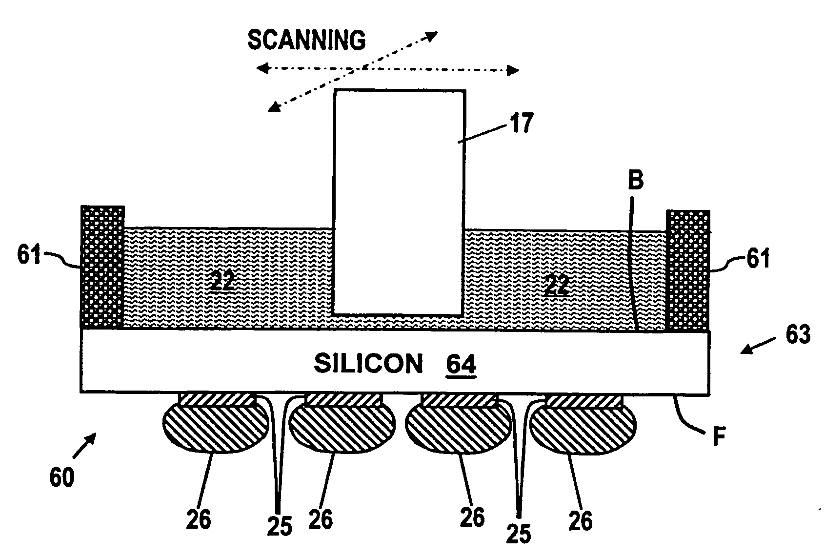
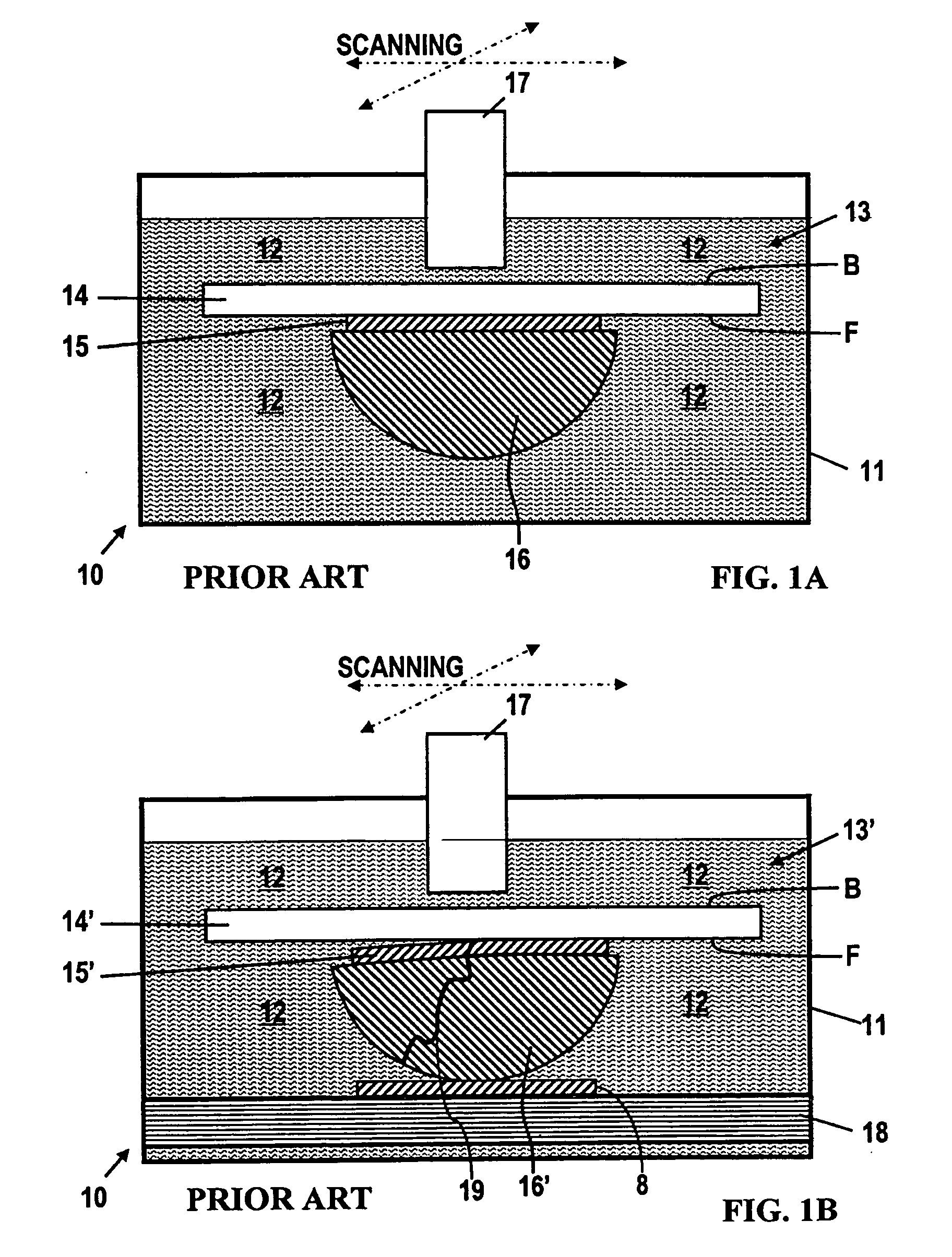
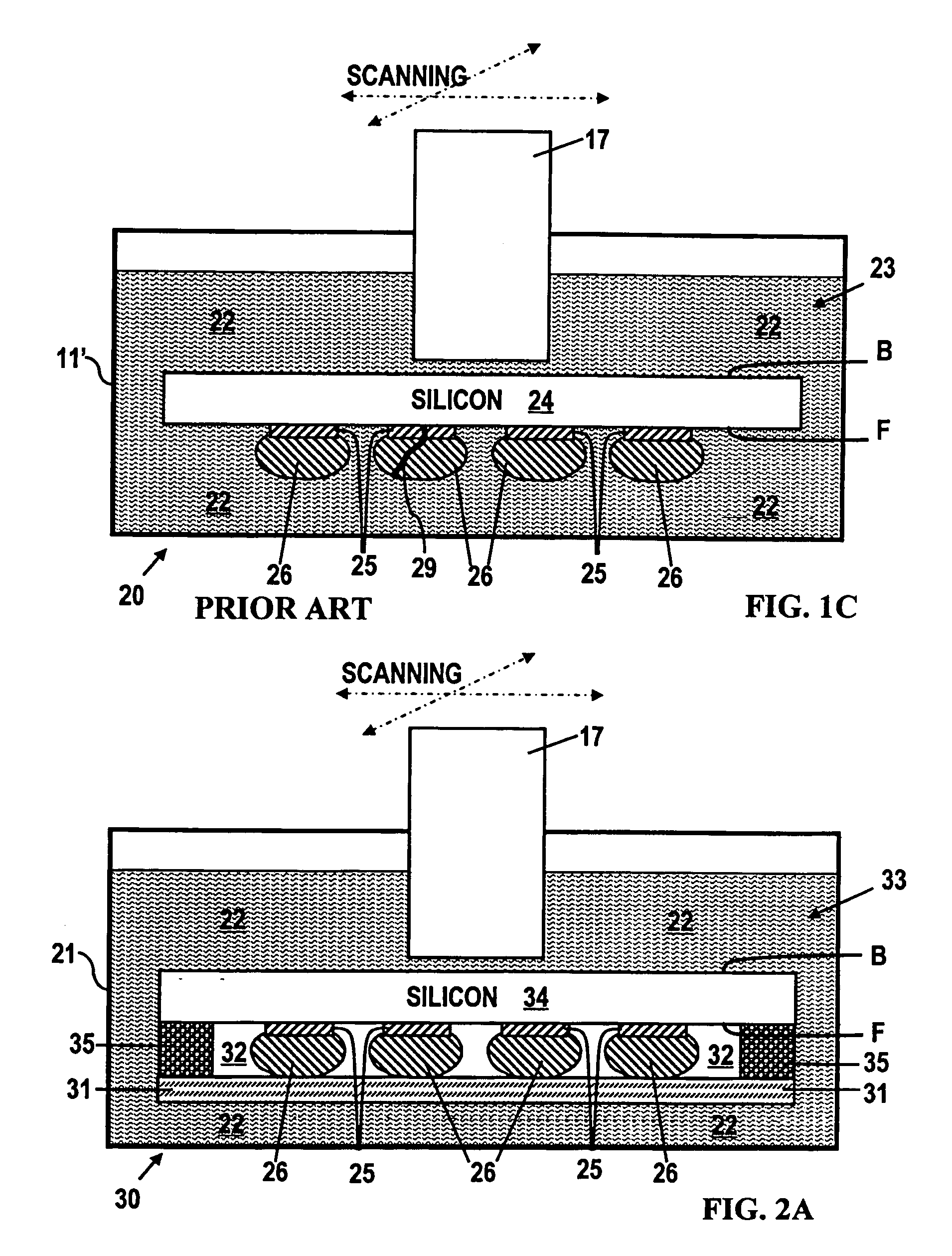
- The method involves isolating BLM pads and C4 solder bumps from the water environment by creating a gas or vacuum chamber around them, using barriers to prevent water intrusion, which enhances the acoustic impedance contrast and allows for non-destructive detection of undercuts and cracks.

System and method for quantifying uniformity patterns for tool development and monitoring
PatentInactiveUS6922603B1
Innovation
- A system and method that objectively quantify nonuniformities by determining multiple metrics, including location and shape, using a mass analogy concept to calculate center of mass, moments of inertia, and defining an ellipsoid to describe the nonuniformity, allowing for precise characterization and correlation with manufacturing process variables.


Semiconductor Industry Standards for Bond Quality Control
The semiconductor industry has established comprehensive standards for bond quality control to ensure reliable wafer-level packaging and three-dimensional integration technologies. These standards primarily focus on quantitative assessment methodologies, defect classification systems, and acceptance criteria that govern the manufacturing processes of bonded semiconductor devices.
SEMI standards, particularly SEMI MF1811 and SEMI MF1535, provide fundamental guidelines for wafer bond interface characterization and defect detection protocols. These specifications define critical parameters including void density thresholds, delamination area limits, and adhesion strength requirements that must be maintained across the entire bonded interface. The standards establish that void areas exceeding 0.1% of the total bond area typically indicate process failures requiring immediate corrective action.
International standards organizations including JEDEC and IPC have developed complementary frameworks addressing bond quality metrics specific to different bonding technologies. JEDEC JESD22-B117 outlines test methods for evaluating bond integrity under thermal cycling conditions, while IPC-9701 establishes performance requirements for direct copper bonding applications. These standards mandate statistical sampling protocols and define acceptable quality levels based on defect density distributions.
Industry-specific quality control standards emphasize the importance of non-destructive testing methodologies for production environments. The standards require that inspection techniques must achieve detection sensitivity levels capable of identifying interfacial defects smaller than 10 micrometers in diameter. Additionally, measurement repeatability specifications demand that bond quality assessments demonstrate coefficient of variation values below 5% across multiple measurement cycles.
Recent updates to semiconductor bonding standards have incorporated advanced acoustic inspection requirements, recognizing the critical role of ultrasonic characterization in modern quality control workflows. These revisions establish minimum frequency requirements, calibration procedures, and data analysis protocols that ensure consistent and reliable bond quality evaluation across different manufacturing facilities and equipment platforms.
SEMI standards, particularly SEMI MF1811 and SEMI MF1535, provide fundamental guidelines for wafer bond interface characterization and defect detection protocols. These specifications define critical parameters including void density thresholds, delamination area limits, and adhesion strength requirements that must be maintained across the entire bonded interface. The standards establish that void areas exceeding 0.1% of the total bond area typically indicate process failures requiring immediate corrective action.
International standards organizations including JEDEC and IPC have developed complementary frameworks addressing bond quality metrics specific to different bonding technologies. JEDEC JESD22-B117 outlines test methods for evaluating bond integrity under thermal cycling conditions, while IPC-9701 establishes performance requirements for direct copper bonding applications. These standards mandate statistical sampling protocols and define acceptable quality levels based on defect density distributions.
Industry-specific quality control standards emphasize the importance of non-destructive testing methodologies for production environments. The standards require that inspection techniques must achieve detection sensitivity levels capable of identifying interfacial defects smaller than 10 micrometers in diameter. Additionally, measurement repeatability specifications demand that bond quality assessments demonstrate coefficient of variation values below 5% across multiple measurement cycles.
Recent updates to semiconductor bonding standards have incorporated advanced acoustic inspection requirements, recognizing the critical role of ultrasonic characterization in modern quality control workflows. These revisions establish minimum frequency requirements, calibration procedures, and data analysis protocols that ensure consistent and reliable bond quality evaluation across different manufacturing facilities and equipment platforms.
Environmental Impact of Advanced Wafer Processing Technologies
The environmental implications of advanced wafer processing technologies, particularly those involving scanning acoustic microscopy for bond adhesion assessment, present a complex landscape of both challenges and opportunities for sustainable semiconductor manufacturing. As the industry continues to push toward smaller geometries and more sophisticated packaging solutions, the environmental footprint of these precision measurement and bonding processes has become increasingly significant.
Energy consumption represents one of the most substantial environmental concerns in acoustic microscopy applications for wafer bond evaluation. High-frequency ultrasonic transducers and sophisticated signal processing systems require considerable electrical power, particularly during extended scanning operations across large wafer surfaces. The computational demands for real-time acoustic data analysis and three-dimensional mapping of adhesion uniformity further amplify energy requirements, contributing to the overall carbon footprint of semiconductor fabrication facilities.
Water usage and chemical consumption in wafer bonding processes present additional environmental challenges. The preparation stages preceding acoustic microscopy evaluation often involve extensive cleaning protocols using deionized water and specialized chemical solutions. Surface activation treatments, essential for achieving optimal bond strength, frequently employ plasma-based processes or wet chemical methods that generate waste streams requiring careful treatment and disposal.
Waste generation from advanced wafer processing extends beyond traditional chemical byproducts to include specialized coupling media used in acoustic microscopy systems. These ultrasonic coupling fluids, while necessary for effective acoustic transmission, must be regularly replaced and properly disposed of to maintain measurement accuracy and prevent contamination.
The manufacturing and lifecycle management of acoustic microscopy equipment itself contributes to environmental impact through material extraction, production processes, and eventual disposal of sophisticated electronic components. High-precision transducers, advanced signal processing hardware, and specialized mechanical scanning systems incorporate rare earth elements and other materials with significant environmental extraction costs.
However, emerging trends toward more environmentally conscious processing approaches are beginning to address these challenges. Development of lower-power acoustic systems, implementation of closed-loop coupling fluid recycling, and integration of artificial intelligence for optimized scanning patterns represent promising directions for reducing environmental impact while maintaining measurement precision and throughput requirements in advanced wafer processing applications.
Energy consumption represents one of the most substantial environmental concerns in acoustic microscopy applications for wafer bond evaluation. High-frequency ultrasonic transducers and sophisticated signal processing systems require considerable electrical power, particularly during extended scanning operations across large wafer surfaces. The computational demands for real-time acoustic data analysis and three-dimensional mapping of adhesion uniformity further amplify energy requirements, contributing to the overall carbon footprint of semiconductor fabrication facilities.
Water usage and chemical consumption in wafer bonding processes present additional environmental challenges. The preparation stages preceding acoustic microscopy evaluation often involve extensive cleaning protocols using deionized water and specialized chemical solutions. Surface activation treatments, essential for achieving optimal bond strength, frequently employ plasma-based processes or wet chemical methods that generate waste streams requiring careful treatment and disposal.
Waste generation from advanced wafer processing extends beyond traditional chemical byproducts to include specialized coupling media used in acoustic microscopy systems. These ultrasonic coupling fluids, while necessary for effective acoustic transmission, must be regularly replaced and properly disposed of to maintain measurement accuracy and prevent contamination.
The manufacturing and lifecycle management of acoustic microscopy equipment itself contributes to environmental impact through material extraction, production processes, and eventual disposal of sophisticated electronic components. High-precision transducers, advanced signal processing hardware, and specialized mechanical scanning systems incorporate rare earth elements and other materials with significant environmental extraction costs.
However, emerging trends toward more environmentally conscious processing approaches are beginning to address these challenges. Development of lower-power acoustic systems, implementation of closed-loop coupling fluid recycling, and integration of artificial intelligence for optimized scanning patterns represent promising directions for reducing environmental impact while maintaining measurement precision and throughput requirements in advanced wafer processing applications.
Unlock deeper insights with PatSnap Eureka Quick Research — get a full tech report to explore trends and direct your research. Try now!
Generate Your Research Report Instantly with AI Agent
Supercharge your innovation with PatSnap Eureka AI Agent Platform!