

Quantify Wafer-Scale Engines' Processing Limits in High Demand
APR 15, 20269 MIN READ
Generate Your Research Report Instantly with AI Agent
Patsnap Eureka helps you evaluate technical feasibility & market potential.
Wafer-Scale Engine Processing Architecture and Performance Goals
Wafer-scale engines represent a paradigm shift in computing architecture, fundamentally reimagining how processing units are designed and interconnected. Unlike traditional chip architectures that rely on discrete processors connected through external networks, wafer-scale engines integrate thousands of processing cores directly onto a single silicon wafer. This approach eliminates the bottlenecks associated with off-chip communication and enables unprecedented levels of parallel processing capability.
The architectural foundation of wafer-scale engines centers on distributed processing elements interconnected through high-bandwidth, low-latency on-chip networks. Each processing core operates semi-independently while maintaining seamless communication with neighboring cores through dedicated interconnect fabric. This mesh-like topology ensures that data can flow efficiently across the entire wafer surface, minimizing communication delays that typically plague traditional multi-chip systems.
Performance goals for wafer-scale engines are ambitious and multifaceted. Primary objectives include achieving petascale computational throughput while maintaining energy efficiency comparable to or exceeding conventional architectures. The target performance metrics encompass raw computational power measured in operations per second, memory bandwidth utilization, and sustained performance under varying workload conditions. These engines aim to deliver consistent performance across diverse computational tasks, from artificial intelligence training to scientific simulations.
Memory hierarchy optimization represents a critical architectural consideration. Wafer-scale engines implement distributed memory systems where each processing core has access to local high-speed memory while sharing access to larger memory pools through the interconnect network. This approach minimizes memory access latency and maximizes bandwidth utilization, addressing one of the most significant performance bottlenecks in traditional computing systems.
Fault tolerance mechanisms are integral to the architectural design, given the scale and complexity of wafer-scale systems. The architecture incorporates redundant processing elements and dynamic reconfiguration capabilities to maintain operational integrity even when individual cores experience failures. This resilience is essential for achieving the reliability standards required for enterprise and scientific computing applications.
Scalability considerations drive the modular design philosophy, where processing capabilities can be dynamically allocated based on workload requirements. The architecture supports heterogeneous computing models, allowing different regions of the wafer to be optimized for specific computational tasks while maintaining overall system coherence and performance efficiency.
Market Demand for Large-Scale AI Computing Infrastructure
The global AI computing infrastructure market is experiencing unprecedented growth driven by the exponential increase in artificial intelligence workloads across multiple industries. Enterprise adoption of large language models, computer vision systems, and deep learning applications has created substantial demand for high-performance computing solutions capable of handling massive parallel processing tasks. Traditional GPU clusters, while effective, face scalability limitations and energy efficiency challenges when deployed at enterprise scale.
Wafer-scale computing engines represent a paradigm shift in addressing these infrastructure demands. Unlike conventional chip architectures that require complex interconnects between multiple processors, wafer-scale engines offer unified computing fabric with dramatically reduced communication latency and higher memory bandwidth. This architectural advantage becomes critical as AI models continue to grow in complexity and parameter count, requiring more sophisticated computational resources.
The financial services sector demonstrates particularly strong demand for large-scale AI infrastructure, utilizing these systems for real-time fraud detection, algorithmic trading, and risk assessment models. Healthcare organizations increasingly rely on AI-powered diagnostic systems and drug discovery platforms that demand sustained high-throughput computing capabilities. Cloud service providers face mounting pressure to deliver AI-as-a-Service offerings with guaranteed performance levels, driving infrastructure investments toward more efficient computing solutions.
Manufacturing and autonomous vehicle development represent emerging high-demand segments where real-time processing requirements exceed traditional computing capabilities. These applications require continuous model training and inference at scale, creating sustained demand for advanced computing infrastructure. The ability to process multiple AI workloads simultaneously on single wafer-scale engines addresses both performance and operational efficiency requirements.
Market dynamics indicate growing preference for integrated solutions that combine high computational density with simplified deployment models. Organizations seek infrastructure that can adapt to varying workload demands while maintaining consistent performance characteristics. This trend favors wafer-scale architectures that offer superior resource utilization compared to distributed computing approaches, particularly for memory-intensive AI applications requiring frequent data access patterns.
Current WSE Processing Bottlenecks and Scalability Challenges
Wafer-Scale Engines face significant processing bottlenecks that fundamentally limit their performance under high computational demand scenarios. The primary constraint stems from memory bandwidth limitations, where the massive parallel processing capabilities of WSE architectures often exceed the data delivery capacity of the memory subsystem. This creates a scenario where thousands of processing elements remain idle while waiting for data, effectively reducing the theoretical peak performance to a fraction of its potential.
Thermal management represents another critical bottleneck that becomes increasingly severe as processing demands intensify. WSE architectures generate substantial heat loads across the entire wafer surface, creating thermal gradients that can exceed safe operating parameters. Current cooling solutions struggle to maintain uniform temperature distribution, leading to thermal throttling that reduces processing frequencies and creates performance inconsistencies across different regions of the wafer.
Power delivery infrastructure poses additional scalability challenges, particularly in sustaining peak performance across all processing elements simultaneously. The power distribution network must handle extreme current densities while maintaining voltage stability, which becomes increasingly difficult as the number of active cores scales up. Voltage droops and power delivery noise can cause processing errors or force conservative operating margins that limit overall throughput.
Interconnect congestion emerges as a fundamental scalability barrier when multiple applications compete for communication resources. The on-chip network fabric, while extensive, experiences bandwidth saturation when handling concurrent high-throughput workloads. This congestion creates unpredictable latencies that can cascade through dependent computations, severely impacting time-sensitive applications and reducing overall system efficiency.
Manufacturing yield variations across the wafer introduce heterogeneous performance characteristics that complicate scalability planning. Different regions of the WSE may exhibit varying processing capabilities due to fabrication tolerances, creating load balancing challenges that prevent optimal resource utilization. These variations become more pronounced as demand increases and the system attempts to utilize every available processing element.
Software orchestration complexity represents a significant challenge in managing resources efficiently across the massive parallel architecture. Current scheduling algorithms struggle to optimize workload distribution while accounting for thermal constraints, power limitations, and interconnect bandwidth availability simultaneously, often resulting in suboptimal performance scaling.
Existing WSE Performance Quantification Methods
01 Wafer-scale integration and multi-chip processing architectures
Wafer-scale engines face processing limits related to integrating multiple processing units or chips on a single wafer substrate. Technologies address the challenges of interconnecting numerous processing elements, managing data flow between chips, and coordinating parallel processing operations across the wafer-scale system. Solutions include specialized interconnection architectures, routing mechanisms, and communication protocols that enable efficient data transfer and synchronization between processing units while minimizing latency and power consumption.- Wafer-scale integration and multi-chip processing architectures: Wafer-scale engines face processing limits related to integrating multiple processing units or chips on a single wafer substrate. Technologies address the challenges of interconnecting numerous processing elements, managing data flow between chips, and coordinating parallel processing operations across the wafer. Solutions include specialized interconnection schemes, routing architectures, and methods for partitioning computational tasks across the wafer-scale system to overcome throughput and bandwidth limitations.
- Thermal management and heat dissipation constraints: Processing limits in wafer-scale engines are significantly impacted by thermal constraints due to the high density of processing elements. Technologies focus on heat dissipation methods, thermal interface materials, cooling system designs, and temperature monitoring mechanisms. Approaches include advanced cooling structures, heat spreaders, and thermal regulation systems that prevent overheating and maintain optimal operating temperatures across the entire wafer to ensure reliable high-performance operation.
- Power distribution and consumption limitations: Wafer-scale processing engines encounter limits related to power delivery and consumption across large-area substrates. Technologies address power distribution networks, voltage regulation, current delivery capabilities, and power consumption optimization. Solutions include specialized power grid designs, multiple power domains, dynamic power management techniques, and methods for reducing power density while maintaining processing performance across the wafer-scale architecture.
- Defect tolerance and yield enhancement mechanisms: Processing limits are influenced by manufacturing defects and yield issues inherent to large-area wafer-scale systems. Technologies provide redundancy schemes, fault-tolerant architectures, defect mapping methods, and reconfiguration capabilities. Approaches include spare processing elements, bypass mechanisms, self-testing circuits, and adaptive routing that allow the system to function despite localized defects, thereby improving overall yield and reliability of wafer-scale engines.
- Interconnect bandwidth and communication bottlenecks: Wafer-scale engines face processing limits due to interconnect bandwidth constraints and communication latency between processing elements. Technologies address high-speed data transfer, network-on-chip architectures, routing protocols, and communication infrastructure optimization. Solutions include advanced interconnect topologies, packet-switching networks, buffering strategies, and bandwidth allocation methods that minimize communication bottlenecks and maximize data throughput across the wafer-scale processing system.
02 Thermal management and heat dissipation in wafer-scale systems
Processing limits in wafer-scale engines are significantly impacted by thermal constraints due to high power density and heat generation across large integrated surfaces. Innovations focus on thermal distribution systems, cooling mechanisms, and heat sink designs that prevent hotspots and maintain uniform temperature across the wafer. Techniques include advanced packaging methods, thermal interface materials, and active cooling solutions that enable sustained high-performance operation without thermal throttling or reliability degradation.Expand Specific Solutions03 Defect tolerance and yield optimization for large-area processing
Wafer-scale engines encounter processing limits due to manufacturing defects that become statistically inevitable across large integrated areas. Technologies implement redundancy schemes, reconfigurable architectures, and fault-tolerant designs that allow systems to function despite the presence of defective components. Methods include spare processing elements, dynamic remapping capabilities, and error detection and correction mechanisms that maintain system performance and improve manufacturing yield despite imperfections in the wafer-scale substrate.Expand Specific Solutions04 Power distribution and consumption management
Processing limits in wafer-scale engines are constrained by power delivery challenges and energy consumption across extensive integrated circuits. Solutions address voltage drop issues, current distribution uniformity, and power supply network design for large-area systems. Innovations include hierarchical power distribution networks, localized voltage regulation, power gating techniques, and dynamic power management strategies that optimize energy efficiency while ensuring stable operation of all processing elements across the wafer-scale platform.Expand Specific Solutions05 Scalability of memory bandwidth and data access
Wafer-scale processing engines face limitations in memory bandwidth and data access patterns that constrain overall system performance. Technologies focus on memory hierarchy optimization, on-chip cache architectures, and high-bandwidth memory interfaces that reduce bottlenecks in data movement. Approaches include distributed memory systems, near-memory processing capabilities, advanced memory controller designs, and innovative data routing schemes that maximize throughput and minimize latency for data-intensive computational workloads across the wafer-scale architecture.Expand Specific Solutions
Key Players in WSE and Large-Scale Processor Industry
The wafer-scale engine processing limits quantification represents an emerging yet rapidly evolving technological frontier within the semiconductor industry. The market is currently in its nascent stage, driven by increasing demand for high-performance computing and AI workloads that require massive parallel processing capabilities. Market size remains relatively small but shows exponential growth potential as hyperscale data centers and AI companies seek alternatives to traditional chip architectures. Technology maturity varies significantly across key players, with established semiconductor manufacturers like Taiwan Semiconductor Manufacturing Co., Intel Corp., and Applied Materials Inc. leading foundational wafer fabrication technologies, while companies such as Advanced Micro Devices and Huawei Technologies are advancing processor architectures. Research institutions including Massachusetts Institute of Technology and Institute of Computing Technology, Chinese Academy of Sciences are contributing fundamental research breakthroughs in wafer-scale computing paradigms, positioning this technology at the intersection of manufacturing capability and computational innovation.
Applied Materials, Inc.
Technical Solution: Applied Materials provides comprehensive wafer-scale processing solutions through their Centura and Producer platforms, capable of handling extreme processing demands with throughput rates exceeding 200 wafers per hour. Their systems integrate advanced process control algorithms and real-time monitoring capabilities to maintain processing consistency across large wafer areas. The company's wafer-scale engines incorporate multi-chamber architectures that enable parallel processing workflows, significantly reducing cycle times while maintaining process uniformity across 300mm substrates under high-demand scenarios.
Strengths: Advanced process control and high-throughput equipment capabilities. Weaknesses: Complex system integration requirements and high maintenance costs for sustained high-demand operations.
Taiwan Semiconductor Manufacturing Co., Ltd.
Technical Solution: TSMC has developed advanced wafer-scale processing capabilities through their CoWoS (Chip on Wafer on Substrate) and InFO (Integrated Fan-Out) packaging technologies. Their wafer-scale engines can handle processing demands up to 300mm wafers with throughput capabilities exceeding 1000 wafers per day for advanced nodes. The company utilizes sophisticated thermal management systems and multi-die integration techniques to maximize processing efficiency while maintaining yield rates above 95% for high-volume production scenarios.
Strengths: Industry-leading manufacturing capacity and yield optimization. Weaknesses: High capital expenditure requirements and dependency on equipment suppliers for scaling limitations.
Core Innovations in WSE Processing Limit Analysis
Diamond enhanced advanced ics and advanced IC packages
PatentActiveUS20230154825A1
Innovation
- The integration of diamond containing layers and bi-wafer microstructures in advanced ICs and SiPs, enabling enhanced thermal conductivity, reduced operating temperatures, and improved interconnect densities through processes like 2.5D interposers, fanout packages, and silicon photonics, which surpass the limitations of silicon-based technologies.


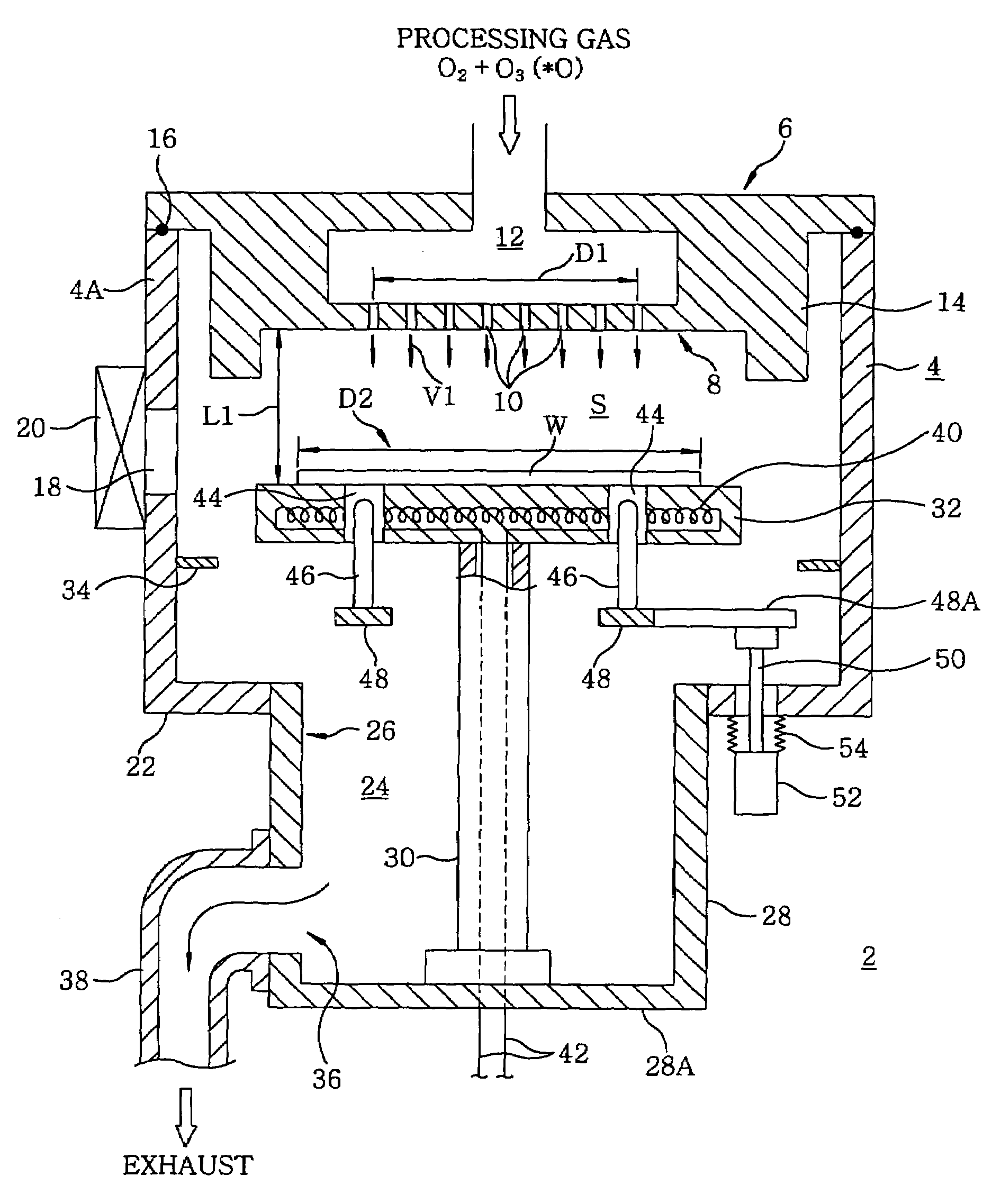
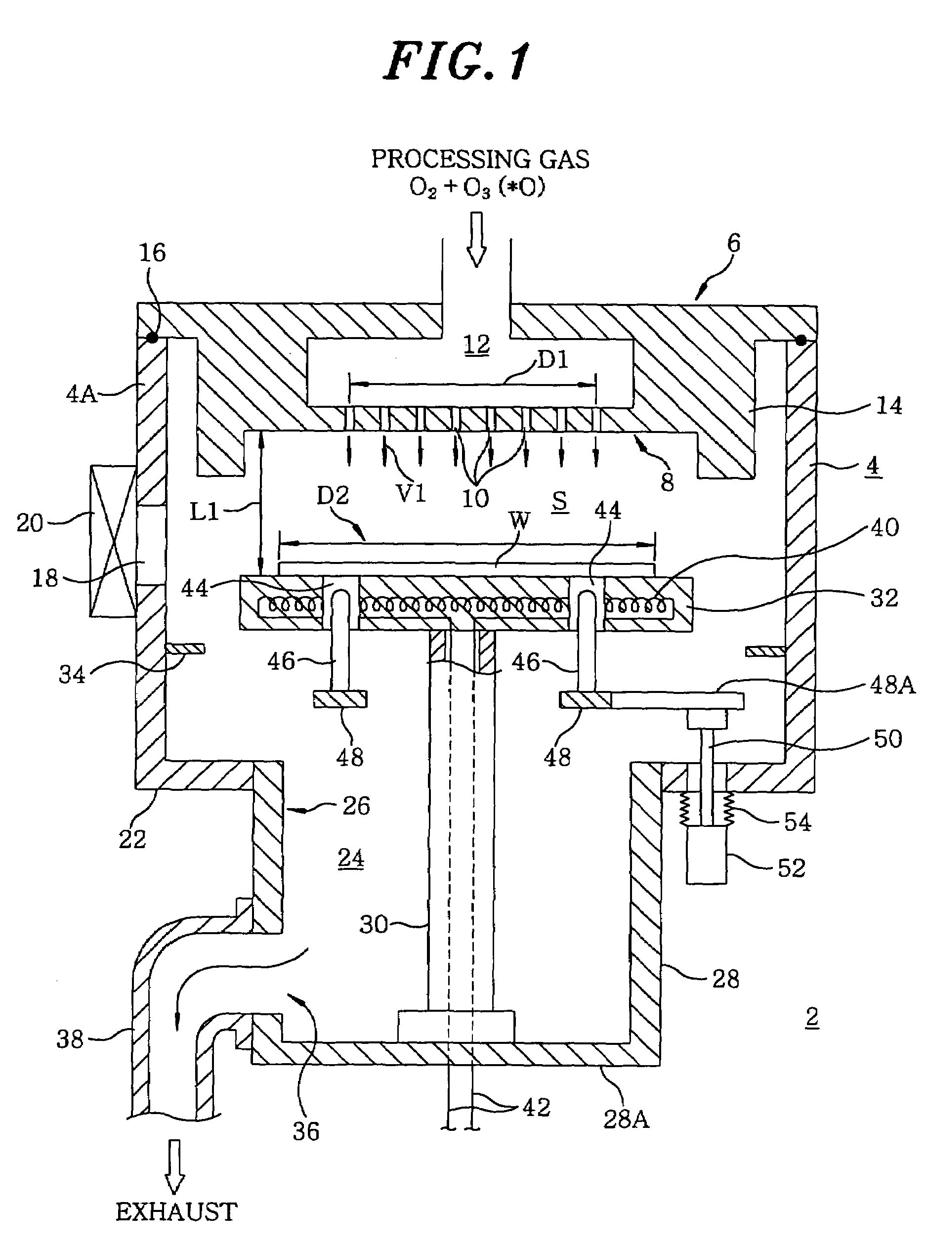
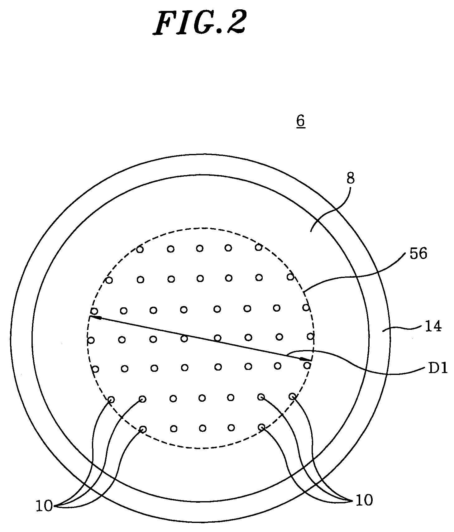
Processing device using shower head structure and processing method
PatentInactiveUS7615251B2
Innovation
- Optimizing the gas jetting velocity and head distance between the shower head and mounting table within a specific range, using a shower head structure with gas jetting holes, to enhance processing efficiency and maintain high within-wafer uniformity.

Thermal Management Standards for WSE Systems
Thermal management in Wafer-Scale Engine (WSE) systems represents a critical engineering challenge that requires comprehensive standardization to ensure reliable operation under high-demand processing scenarios. The unprecedented scale of WSE architectures, containing hundreds of thousands of processing cores on a single silicon wafer, generates substantial heat densities that far exceed conventional processor thermal profiles. Current industry standards primarily address traditional chip-scale thermal management, leaving significant gaps in addressing wafer-scale thermal dynamics.
The establishment of thermal management standards for WSE systems must encompass multiple operational parameters including maximum junction temperatures, thermal gradient tolerances, and cooling system specifications. Industry consensus suggests that WSE systems should maintain core temperatures below 85°C under peak computational loads, with thermal variations across the wafer surface not exceeding 10°C to prevent performance degradation and reliability issues. These standards require sophisticated monitoring systems capable of real-time temperature mapping across thousands of sensor points distributed throughout the wafer substrate.
Cooling infrastructure standards for WSE systems demand advanced liquid cooling solutions with precise flow rate specifications and coolant temperature control. The recommended approach involves direct liquid cooling with flow rates exceeding 20 liters per minute and inlet temperatures maintained between 15-25°C. Heat dissipation capabilities must accommodate power densities reaching 15-20 kW per wafer, significantly higher than traditional server cooling requirements.
Standardized thermal interface materials and heat spreader designs are essential components of WSE thermal management protocols. These standards specify thermal conductivity requirements exceeding 400 W/mK for interface materials and mandate uniform heat distribution mechanisms to prevent localized hotspots. Additionally, thermal cycling standards must address the unique challenges of wafer-scale expansion and contraction, establishing acceptable stress limits to maintain structural integrity during temperature fluctuations.
Environmental control standards extend beyond the immediate cooling system to encompass data center infrastructure requirements, including ambient temperature control, humidity management, and airflow optimization. These comprehensive thermal management standards form the foundation for reliable WSE deployment in high-demand computational environments, ensuring sustained performance while protecting substantial hardware investments.
Power Consumption Constraints in WSE Deployment
Power consumption represents the most critical constraint limiting WSE deployment scalability in high-demand computational environments. Current wafer-scale engines consume between 15-20 kilowatts per unit under peak operational loads, creating substantial infrastructure requirements that extend beyond traditional data center capabilities. This power density, approximately 10-15 times higher than conventional GPU clusters, necessitates specialized cooling systems and dedicated power distribution networks.
Thermal management emerges as the primary bottleneck in WSE power optimization. The concentrated heat generation across the wafer surface creates localized hotspots that can exceed 85°C, forcing dynamic frequency scaling and performance throttling. Advanced liquid cooling solutions, including direct-to-chip and immersion cooling technologies, become mandatory rather than optional, adding 20-30% to total deployment costs.
Power delivery infrastructure poses significant challenges for large-scale WSE installations. Each unit requires dedicated 480V three-phase power connections with specialized power conditioning equipment to maintain voltage stability within 2% tolerance. Data centers must undergo substantial electrical infrastructure upgrades, including transformer capacity expansion and backup power system modifications, to support multiple WSE deployments.
Dynamic power scaling mechanisms currently limit sustained peak performance capabilities. WSE systems implement aggressive power management protocols that reduce computational throughput by 15-25% during extended high-demand periods to prevent thermal violations. This constraint becomes particularly problematic in continuous inference workloads where sustained performance is critical for meeting service level agreements.
Energy efficiency optimization remains an active area of development, with current WSE architectures achieving 2-3 TOPS per watt under optimal conditions. However, real-world efficiency drops significantly during mixed workloads and memory-intensive operations, highlighting the need for improved power management algorithms and hardware-level optimizations to maximize computational output within existing power budgets.
Unlock deeper insights with Patsnap Eureka Quick Research — get a full tech report to explore trends and direct your research. Try now!
Generate Your Research Report Instantly with AI Agent
Supercharge your innovation with Patsnap Eureka AI Agent Platform!