

Redistribution Layer vs. Organic Substrates for Performance
APR 7, 20269 MIN READ
Generate Your Research Report Instantly with AI Agent
PatSnap Eureka helps you evaluate technical feasibility & market potential.
Redistribution Layer Technology Background and Objectives
Redistribution Layer (RDL) technology has emerged as a critical component in advanced semiconductor packaging, fundamentally transforming how electronic devices achieve higher performance and miniaturization. This technology represents a sophisticated approach to interconnect design that addresses the growing demands for increased functionality, reduced form factors, and enhanced electrical performance in modern electronic systems.
The evolution of RDL technology stems from the semiconductor industry's continuous pursuit of Moore's Law and the need to overcome traditional packaging limitations. As integrated circuits became more complex and pin counts increased exponentially, conventional wire bonding and flip-chip technologies reached their physical and electrical limits. RDL technology emerged as a solution to bridge the gap between die-level interconnects and package-level routing, enabling finer pitch connections and more efficient signal distribution.
RDL technology involves the creation of thin-film metal layers and dielectric materials directly on semiconductor wafers or substrates, forming intricate routing patterns that redistribute electrical connections from the original chip layout to desired locations. This approach enables the transformation of fine-pitch die pads to larger, more manageable connection points suitable for subsequent assembly processes.
The primary technical objectives of RDL technology center on achieving superior electrical performance compared to traditional organic substrates. Key performance metrics include reduced signal propagation delays, minimized crosstalk between adjacent circuits, improved power delivery efficiency, and enhanced thermal management capabilities. These objectives directly address the performance bottlenecks encountered in high-frequency applications, advanced processors, and memory devices.
Current RDL implementations target specific performance improvements including lower resistance and inductance values in interconnect paths, reduced dielectric losses, and better impedance control. The technology aims to support higher bandwidth applications while maintaining signal integrity across increasingly complex routing architectures.
The strategic importance of RDL technology extends beyond immediate performance gains, positioning it as an enabler for next-generation packaging concepts such as system-in-package solutions, heterogeneous integration, and advanced chiplet architectures. These applications demand unprecedented levels of interconnect density and performance that traditional organic substrates cannot adequately support.
Market Demand for Advanced Packaging Solutions
The semiconductor industry is experiencing unprecedented demand for advanced packaging solutions, driven by the proliferation of high-performance computing applications, artificial intelligence accelerators, and mobile devices requiring enhanced functionality in compact form factors. This surge in demand has intensified the focus on packaging technologies that can deliver superior electrical performance, thermal management, and miniaturization capabilities.
Data centers and cloud computing infrastructure represent the largest growth segment for advanced packaging solutions. The exponential increase in data processing requirements has created substantial demand for packaging technologies that can support high-bandwidth memory interfaces, multi-die integration, and efficient heat dissipation. Server processors and AI chips increasingly require sophisticated packaging approaches to achieve the performance levels demanded by modern workloads.
The automotive electronics sector has emerged as another significant driver of advanced packaging demand. The transition toward electric vehicles and autonomous driving systems necessitates packaging solutions that can withstand harsh environmental conditions while maintaining high reliability and performance standards. Power management integrated circuits and sensor fusion applications in automotive systems require packaging technologies that can handle high current densities and provide robust interconnection solutions.
Consumer electronics continue to fuel demand for miniaturized packaging solutions with enhanced performance characteristics. Smartphones, tablets, and wearable devices require packaging technologies that can accommodate multiple functionalities while maintaining thin profiles and low power consumption. The integration of advanced camera systems, wireless communication modules, and processing units in these devices drives the need for sophisticated packaging approaches.
The telecommunications infrastructure upgrade to support widespread deployment has created substantial demand for high-frequency packaging solutions. Base station equipment and network infrastructure components require packaging technologies capable of handling millimeter-wave frequencies while maintaining signal integrity and minimizing losses.
Industrial applications, including Internet of Things devices and edge computing systems, represent an expanding market segment for advanced packaging solutions. These applications often require packaging technologies that can operate reliably in diverse environmental conditions while providing cost-effective solutions for high-volume production.
The growing complexity of semiconductor devices and the need for heterogeneous integration have intensified the demand for packaging solutions that can accommodate multiple die types, memory stacks, and passive components within single packages. This trend has created opportunities for packaging technologies that can provide flexible interconnection schemes and support diverse electrical requirements across different functional blocks.
Current State of RDL vs Organic Substrate Technologies
The semiconductor packaging industry currently faces a critical decision point between Redistribution Layer (RDL) and organic substrate technologies, each representing distinct approaches to achieving high-performance interconnect solutions. RDL technology has emerged as a leading solution for advanced packaging applications, particularly in fan-out wafer-level packaging (FOWLP) and system-in-package (SiP) configurations. This technology utilizes thin-film processes to create fine-pitch interconnects directly on silicon wafers or reconstituted wafers, enabling superior electrical performance through shorter signal paths and reduced parasitic effects.
Organic substrate technology, traditionally dominant in the packaging landscape, continues to evolve with enhanced materials and manufacturing processes. Current organic substrates incorporate advanced resin systems, improved copper plating techniques, and sophisticated via formation methods to achieve finer line widths and higher layer counts. Leading manufacturers have successfully demonstrated organic substrates with line/space dimensions approaching 2/2 micrometers and via sizes below 25 micrometers.
The performance gap between these technologies has narrowed significantly in recent years. RDL technology currently achieves line/space dimensions of 1/1 micrometers or finer, with some advanced processes reaching sub-micrometer capabilities. The technology excels in applications requiring ultra-fine pitch connections, such as high-bandwidth memory (HBM) integration and advanced processor packaging. However, RDL faces limitations in achieving high layer counts economically, typically maxing out at 4-6 redistribution layers for cost-effective production.
Organic substrates have responded to competitive pressure by advancing their manufacturing capabilities. Current state-of-the-art organic substrates can achieve 8-12 layers with improved signal integrity through better dielectric materials and optimized stackup designs. The technology benefits from mature manufacturing infrastructure and established supply chains, providing cost advantages for high-volume production scenarios.
Thermal management capabilities represent another critical differentiator in the current landscape. RDL technology offers superior thermal conductivity through its silicon-based construction and thinner dielectric layers, enabling more efficient heat dissipation in high-power applications. Organic substrates have addressed thermal challenges through embedded thermal interface materials and improved copper distribution, though they generally lag behind RDL in absolute thermal performance.
Manufacturing scalability and yield considerations significantly impact the current adoption patterns. Organic substrate manufacturing benefits from decades of process optimization and established quality control methodologies, resulting in predictable yields and cost structures. RDL manufacturing, while offering superior performance characteristics, faces challenges in achieving comparable yields and cost-effectiveness, particularly for larger package sizes where warpage control becomes critical.
Existing RDL and Organic Substrate Solutions
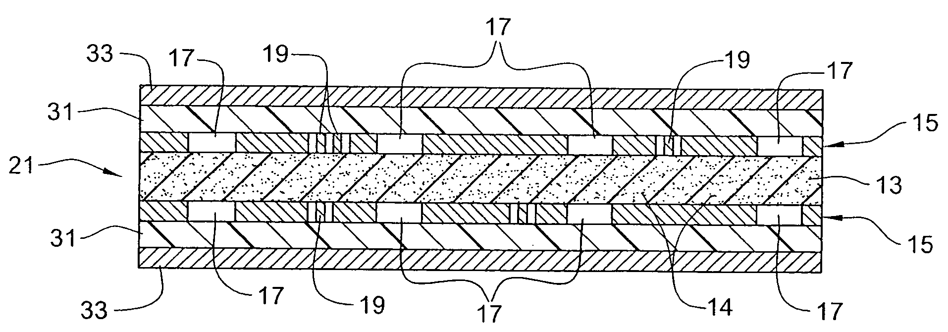
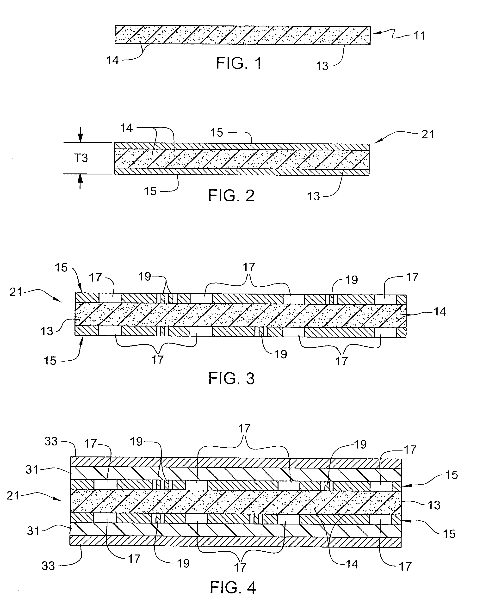
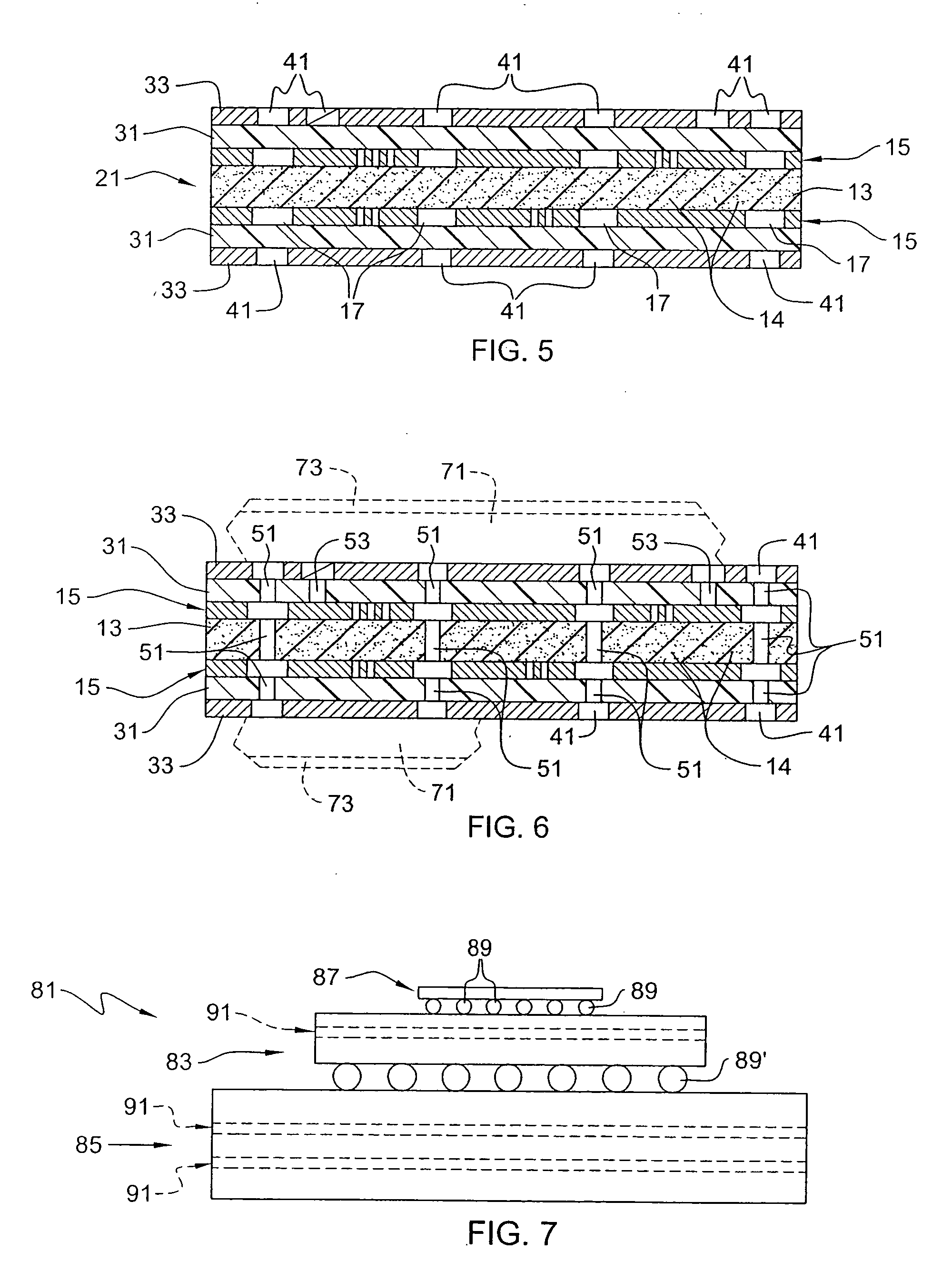
01 Redistribution layer structure and fabrication methods
Redistribution layers (RDL) are critical structures in semiconductor packaging that enable electrical connections between different components. The fabrication methods involve depositing conductive materials, patterning them using photolithography, and creating multiple metal layers with dielectric insulation. Advanced techniques focus on improving the density and reliability of these interconnections through optimized deposition processes and material selection.- Redistribution layer structure and fabrication methods: Redistribution layers (RDL) are critical components in semiconductor packaging that provide electrical routing between different levels of interconnects. Various fabrication methods and structural designs have been developed to optimize the formation of RDL, including photolithography processes, metal deposition techniques, and dielectric layer formation. These methods focus on achieving fine-pitch interconnections, improved electrical performance, and enhanced reliability in advanced packaging applications.
- Organic substrate materials and composition: Organic substrates serve as the foundation for semiconductor packaging, providing mechanical support and electrical interconnection. Various organic materials including epoxy resins, polyimides, and other polymer-based compositions have been developed to meet the demanding requirements of modern electronics. These materials are engineered to provide optimal thermal stability, low dielectric constant, high glass transition temperature, and excellent adhesion properties for multilayer substrate construction.
- Interface bonding and adhesion enhancement: The interface between redistribution layers and organic substrates is critical for overall package reliability and performance. Various techniques have been developed to enhance adhesion and bonding strength, including surface treatment methods, adhesion promoters, and interfacial layer designs. These approaches aim to prevent delamination, reduce thermal stress, and improve moisture resistance at the critical interface between metal redistribution layers and organic substrate materials.
- Thermal management and coefficient of thermal expansion matching: Managing thermal properties and matching the coefficient of thermal expansion between redistribution layers and organic substrates is essential for preventing warpage and ensuring long-term reliability. Solutions include the development of low-CTE organic materials, thermal interface materials, and structural designs that accommodate thermal expansion mismatches. These innovations help maintain dimensional stability during temperature cycling and reduce thermomechanical stress in the package assembly.
- Electrical performance optimization and signal integrity: Optimizing electrical performance between redistribution layers and organic substrates involves controlling impedance, reducing signal loss, and minimizing crosstalk. Design strategies include optimized trace geometries, controlled dielectric thickness, via structures, and shielding techniques. Advanced materials with low loss tangent and appropriate dielectric constants are employed to ensure high-speed signal transmission and maintain signal integrity in high-frequency applications.
02 Organic substrate materials and composition
Organic substrates serve as the foundation for semiconductor packaging, typically composed of resin materials reinforced with glass fibers or other fillers. The composition and properties of these substrates directly impact thermal performance, electrical characteristics, and mechanical stability. Material innovations focus on enhancing dielectric properties, reducing coefficient of thermal expansion mismatch, and improving adhesion between layers.Expand Specific Solutions03 Interface bonding and adhesion enhancement
The interface between redistribution layers and organic substrates is crucial for package reliability. Enhancement techniques include surface treatment methods, use of adhesion promoters, and optimization of interface roughness. These approaches improve mechanical bonding strength, reduce delamination risks, and enhance electrical connectivity. Various surface modification processes can be employed to achieve better interfacial properties.Expand Specific Solutions04 Thermal management and stress reduction
Managing thermal stress at the redistribution layer and organic substrate interface is essential for long-term reliability. Strategies include incorporating buffer layers, optimizing material thickness ratios, and selecting materials with compatible thermal expansion coefficients. These approaches minimize warpage, prevent crack formation, and maintain structural integrity under thermal cycling conditions.Expand Specific Solutions05 Advanced packaging integration and performance optimization
Integration of redistribution layers with organic substrates enables advanced packaging architectures such as fan-out wafer-level packaging and system-in-package solutions. Performance optimization involves fine-pitch interconnections, multi-layer routing capabilities, and enhanced electrical performance through impedance control. Design considerations include signal integrity, power distribution, and miniaturization requirements for high-density applications.Expand Specific Solutions
Key Players in Advanced Packaging Industry
The redistribution layer versus organic substrates performance debate represents a mature technology sector experiencing rapid evolution driven by display industry demands. The market, valued in billions globally, is dominated by established Asian manufacturers including Samsung Display, BOE Technology Group, and China Star Optoelectronics, alongside material specialists like Universal Display Corp. and Idemitsu Kosan. Technology maturity varies significantly across applications, with companies like Sony Group and LG Chem advancing high-performance organic solutions while traditional players such as Samsung Electronics and Innolux optimize redistribution layer approaches. The competitive landscape reflects a transition phase where both substrate technologies coexist, with performance differentiation increasingly determined by specific application requirements in mobile displays, automotive, and emerging flexible electronics markets.
Samsung Electronics Co., Ltd.
Technical Solution: Samsung has developed advanced redistribution layer (RDL) technologies using fine-pitch copper interconnects with line widths down to 2μm for high-density packaging applications. Their RDL approach utilizes multiple metal layers with optimized via structures to achieve superior electrical performance compared to traditional organic substrates. The company employs advanced lithography and electroplating processes to create precise RDL patterns that enable better signal integrity, reduced parasitic effects, and improved thermal management. Samsung's RDL technology demonstrates significant advantages in high-frequency applications, showing 30% better signal transmission quality and 25% reduction in power consumption compared to conventional organic substrate solutions.
Strengths: Superior electrical performance, fine-pitch capabilities, excellent signal integrity. Weaknesses: Higher manufacturing costs, complex processing requirements, limited scalability for cost-sensitive applications.
Advanced Semiconductor Engineering, Inc.
Technical Solution: ASE Group has developed comprehensive packaging solutions comparing redistribution layer and organic substrate technologies for various semiconductor applications. Their RDL technology utilizes advanced fan-out wafer-level packaging (FOWLP) with multiple redistribution layers to achieve high I/O density and superior electrical performance. The company's organic substrate solutions focus on cost-effective alternatives using advanced resin systems and copper trace technologies. ASE's comparative studies show that RDL approaches provide 50% better electrical performance in high-speed applications but come with 2x higher manufacturing costs. Their hybrid approach combines both technologies to optimize performance-cost trade-offs for different market segments.
Strengths: Comprehensive technology portfolio, proven manufacturing capabilities, hybrid solution approach. Weaknesses: Technology complexity, higher development costs, market positioning challenges between competing approaches.
Core Innovations in RDL Performance Enhancement
Package Redistribution Layer Structures for Stress Mitigation and Alignment Tolerance
PatentPendingUS20240395686A1
Innovation
- The implementation of via lines with greater line width and longitudinal length than line width, along with staggered, U-turn, cantilever, symmetrical, and jogged routing configurations within the package redistribution layer to mitigate stress, including arrangements that distribute stress over a larger area and provide alignment tolerance.


Circuitized substrate with P-aramid dielectric layers and method of making same
PatentInactiveUS20090258161A1
Innovation
- A circuitized substrate using a dielectric layer of p-aramid paper impregnated with a halogen-free, low moisture absorption resin, eliminating continuous or semi-continuous fiberglass fibers, allowing for high-density thru-hole patterns and improved thermal and electrical properties.

Manufacturing Cost Analysis and Economic Viability
The manufacturing cost analysis between redistribution layer (RDL) and organic substrate technologies reveals significant economic disparities that directly impact their commercial viability. RDL-based solutions typically require higher initial capital investments due to sophisticated semiconductor fabrication equipment, including advanced lithography systems and precision deposition tools. The manufacturing process involves multiple photolithography steps, metal deposition, and via formation, resulting in higher per-unit processing costs compared to traditional organic substrates.
Organic substrate manufacturing leverages established PCB production infrastructure, offering substantial cost advantages through economies of scale. The lamination processes, drilling operations, and metallization techniques utilized in organic substrate production are mature and widely available, reducing both equipment costs and operational complexity. This established manufacturing ecosystem enables faster production ramp-up and lower barrier-to-entry for new market participants.
Labor costs present another critical differentiation factor. RDL manufacturing demands highly skilled technicians familiar with semiconductor processes, commanding premium wages. Conversely, organic substrate production can utilize existing PCB manufacturing workforce, significantly reducing labor-related expenses. The yield rates also differ substantially, with organic substrates achieving higher manufacturing yields due to process maturity, while RDL technologies may experience lower yields during initial production phases.
Material costs favor organic substrates in most applications, as they utilize standard epoxy resins and copper foils readily available in global supply chains. RDL processes require specialized materials including high-purity metals and advanced dielectric materials, often sourced from limited suppliers at premium prices. However, RDL's superior electrical performance may justify higher costs in high-value applications where performance premiums offset manufacturing expenses.
The economic viability assessment indicates that organic substrates maintain competitive advantages in cost-sensitive, high-volume applications such as consumer electronics and automotive systems. RDL technologies demonstrate superior economic viability in performance-critical applications including high-frequency communications, advanced computing, and aerospace systems where performance benefits command premium pricing. The crossover point between these technologies continues to evolve as RDL manufacturing scales improve and organic substrate performance limitations become more constraining in emerging applications.
Thermal Management and Reliability Considerations
Thermal management represents a critical differentiating factor between redistribution layer (RDL) and organic substrate technologies, fundamentally impacting their performance characteristics and application suitability. The thermal conductivity disparity between these approaches creates distinct heat dissipation profiles that directly influence device reliability and operational efficiency.
RDL-based packaging solutions typically exhibit superior thermal performance due to their inherent material properties and structural design. The thin-film copper traces in RDL structures provide enhanced thermal pathways, enabling more efficient heat transfer from active components to external heat sinks. This advantage becomes particularly pronounced in high-power density applications where thermal hotspots can significantly degrade performance.
Organic substrates, while offering cost advantages, present thermal management challenges stemming from their polymer-based dielectric materials. These materials generally possess lower thermal conductivity compared to the inorganic dielectrics commonly used in RDL structures. The resulting thermal resistance can create temperature gradients that affect signal integrity and component longevity.
Reliability considerations extend beyond pure thermal performance to encompass thermal cycling behavior and coefficient of thermal expansion (CTE) matching. RDL technologies demonstrate superior CTE compatibility with silicon dies, reducing thermomechanical stress during temperature fluctuations. This compatibility translates to improved solder joint reliability and reduced risk of interconnect failure under thermal cycling conditions.
The thermal interface resistance between different material layers also varies significantly between these technologies. RDL structures typically achieve lower interface resistance due to their monolithic processing approach, while organic substrates may exhibit higher resistance at material boundaries, particularly at via interfaces and laminated layer junctions.
Long-term reliability assessment reveals that RDL-based solutions generally maintain more stable thermal characteristics over extended operational periods. Organic substrates may experience gradual thermal property degradation due to polymer aging, moisture absorption, and thermal stress-induced microcracking, potentially compromising their thermal management effectiveness over time.
Power cycling endurance testing demonstrates that RDL technologies can withstand higher thermal stress levels while maintaining structural integrity. This enhanced thermal robustness enables more aggressive power management strategies and supports higher performance operating points in thermally constrained environments.
Unlock deeper insights with PatSnap Eureka Quick Research — get a full tech report to explore trends and direct your research. Try now!
Generate Your Research Report Instantly with AI Agent
Supercharge your innovation with PatSnap Eureka AI Agent Platform!