

Redistribution Layer vs Wafer Level Packaging: Benefits/Limitations
APR 7, 20269 MIN READ
Generate Your Research Report Instantly with AI Agent
PatSnap Eureka helps you evaluate technical feasibility & market potential.
RDL and WLP Technology Background and Objectives
Redistribution Layer (RDL) and Wafer Level Packaging (WLP) technologies represent critical advancements in semiconductor packaging, emerging from the industry's relentless pursuit of miniaturization, enhanced performance, and cost-effective manufacturing solutions. These technologies have evolved as direct responses to the limitations of traditional wire bonding and flip-chip packaging methods, which struggled to meet the demanding requirements of modern electronic devices.
The development trajectory of RDL technology began in the late 1990s as semiconductor manufacturers sought alternatives to conventional packaging approaches. Initially conceived as a method to redistribute electrical connections from chip pads to different locations on the package substrate, RDL has evolved into a sophisticated platform enabling complex routing architectures and multi-functional integration capabilities.
WLP technology emerged concurrently, driven by the need to eliminate traditional packaging substrates and reduce overall package footprint. This approach performs packaging operations directly at the wafer level before individual die separation, fundamentally transforming the packaging paradigm from a post-dicing process to an integral part of wafer fabrication.
The convergence of these technologies has been accelerated by several market drivers, including the proliferation of mobile devices, Internet of Things applications, and automotive electronics. These sectors demand increasingly compact form factors while maintaining or improving electrical performance, thermal management, and reliability standards.
Current technological objectives focus on achieving finer pitch capabilities, with industry targets pushing toward sub-10 micron line widths and spacing in RDL structures. Advanced WLP implementations aim to integrate multiple die types, passive components, and even MEMS devices within single packages, creating system-in-package solutions that rival traditional multi-chip modules.
The evolution has also been shaped by material science advances, particularly in polymer dielectrics, seed layer technologies, and plating chemistries. These developments enable thinner profiles, improved electrical characteristics, and enhanced mechanical reliability under various stress conditions.
Manufacturing scalability remains a primary objective, with industry efforts concentrated on developing processes compatible with standard semiconductor fabrication equipment while maintaining cost competitiveness against traditional packaging methods. This includes optimizing lithography processes, developing efficient metallization techniques, and establishing robust quality control methodologies for high-volume production environments.
The development trajectory of RDL technology began in the late 1990s as semiconductor manufacturers sought alternatives to conventional packaging approaches. Initially conceived as a method to redistribute electrical connections from chip pads to different locations on the package substrate, RDL has evolved into a sophisticated platform enabling complex routing architectures and multi-functional integration capabilities.
WLP technology emerged concurrently, driven by the need to eliminate traditional packaging substrates and reduce overall package footprint. This approach performs packaging operations directly at the wafer level before individual die separation, fundamentally transforming the packaging paradigm from a post-dicing process to an integral part of wafer fabrication.
The convergence of these technologies has been accelerated by several market drivers, including the proliferation of mobile devices, Internet of Things applications, and automotive electronics. These sectors demand increasingly compact form factors while maintaining or improving electrical performance, thermal management, and reliability standards.
Current technological objectives focus on achieving finer pitch capabilities, with industry targets pushing toward sub-10 micron line widths and spacing in RDL structures. Advanced WLP implementations aim to integrate multiple die types, passive components, and even MEMS devices within single packages, creating system-in-package solutions that rival traditional multi-chip modules.
The evolution has also been shaped by material science advances, particularly in polymer dielectrics, seed layer technologies, and plating chemistries. These developments enable thinner profiles, improved electrical characteristics, and enhanced mechanical reliability under various stress conditions.
Manufacturing scalability remains a primary objective, with industry efforts concentrated on developing processes compatible with standard semiconductor fabrication equipment while maintaining cost competitiveness against traditional packaging methods. This includes optimizing lithography processes, developing efficient metallization techniques, and establishing robust quality control methodologies for high-volume production environments.
Market Demand Analysis for Advanced Packaging Solutions
The global semiconductor packaging market is experiencing unprecedented growth driven by the proliferation of mobile devices, Internet of Things applications, and artificial intelligence systems. Advanced packaging technologies, particularly redistribution layer and wafer level packaging solutions, have emerged as critical enablers for meeting the stringent requirements of modern electronic systems. The demand for these technologies stems from the industry's relentless pursuit of miniaturization, enhanced performance, and cost optimization.
Mobile and consumer electronics represent the largest market segment driving demand for advanced packaging solutions. Smartphones, tablets, and wearable devices require increasingly compact form factors while delivering superior functionality. This has created substantial market pull for wafer level packaging technologies, which offer the smallest possible package footprint and enable direct chip-to-board assembly. The automotive electronics sector has also become a significant demand driver, particularly with the rise of electric vehicles and autonomous driving systems that require high-performance computing capabilities in harsh operating environments.
Data center and high-performance computing applications constitute another major market segment fueling demand for redistribution layer technologies. These applications prioritize electrical performance, thermal management, and high-density interconnections over absolute miniaturization. The growing adoption of artificial intelligence, machine learning, and cloud computing services has intensified requirements for advanced packaging solutions that can support complex multi-chip configurations and heterogeneous integration.
The telecommunications infrastructure market, particularly with the global rollout of 5G networks, has generated substantial demand for both packaging approaches. Base station equipment, network processors, and radio frequency components require packaging solutions that can handle high-frequency signals while maintaining signal integrity and thermal performance. This market segment values the superior electrical characteristics that redistribution layer technologies can provide.
Emerging applications in healthcare, industrial automation, and edge computing are creating new market opportunities for advanced packaging solutions. Medical devices demand ultra-miniaturized packages with high reliability, while industrial applications require robust packaging that can withstand extreme environmental conditions. Edge computing applications seek optimal balance between performance, power efficiency, and cost-effectiveness, driving demand for innovative packaging approaches that can accommodate diverse system requirements across multiple market verticals.
Mobile and consumer electronics represent the largest market segment driving demand for advanced packaging solutions. Smartphones, tablets, and wearable devices require increasingly compact form factors while delivering superior functionality. This has created substantial market pull for wafer level packaging technologies, which offer the smallest possible package footprint and enable direct chip-to-board assembly. The automotive electronics sector has also become a significant demand driver, particularly with the rise of electric vehicles and autonomous driving systems that require high-performance computing capabilities in harsh operating environments.
Data center and high-performance computing applications constitute another major market segment fueling demand for redistribution layer technologies. These applications prioritize electrical performance, thermal management, and high-density interconnections over absolute miniaturization. The growing adoption of artificial intelligence, machine learning, and cloud computing services has intensified requirements for advanced packaging solutions that can support complex multi-chip configurations and heterogeneous integration.
The telecommunications infrastructure market, particularly with the global rollout of 5G networks, has generated substantial demand for both packaging approaches. Base station equipment, network processors, and radio frequency components require packaging solutions that can handle high-frequency signals while maintaining signal integrity and thermal performance. This market segment values the superior electrical characteristics that redistribution layer technologies can provide.
Emerging applications in healthcare, industrial automation, and edge computing are creating new market opportunities for advanced packaging solutions. Medical devices demand ultra-miniaturized packages with high reliability, while industrial applications require robust packaging that can withstand extreme environmental conditions. Edge computing applications seek optimal balance between performance, power efficiency, and cost-effectiveness, driving demand for innovative packaging approaches that can accommodate diverse system requirements across multiple market verticals.
Current Status and Challenges in RDL vs WLP Technologies
The current landscape of Redistribution Layer (RDL) and Wafer Level Packaging (WLP) technologies presents a complex competitive environment where both approaches have achieved significant maturity while facing distinct technical and economic challenges. RDL technology has established itself as a dominant force in advanced packaging, particularly for high-performance computing and mobile applications, with major foundries like TSMC, Samsung, and Intel offering sophisticated multi-layer RDL solutions. These implementations typically feature line widths ranging from 2-10 micrometers and support complex routing architectures with up to 10 or more metal layers.
WLP technology has simultaneously evolved along parallel tracks, with Fan-Out Wafer Level Packaging (FOWLP) emerging as a particularly competitive alternative. Companies such as ASE Group, Amkor, and JCET have developed robust WLP manufacturing capabilities that can achieve similar electrical performance to RDL while potentially offering cost advantages for certain applications. The technology has demonstrated particular strength in mobile processors and RF applications where form factor constraints are critical.
Current technical challenges in RDL implementation center around thermal management, signal integrity at high frequencies, and manufacturing yield optimization. The multi-layer nature of RDL structures creates complex thermal pathways that can lead to hotspot formation, particularly in high-power applications. Additionally, achieving consistent via formation and metal layer adhesion across large wafers remains a significant manufacturing challenge, with yield rates varying considerably based on design complexity and feature density.
WLP faces its own set of technical hurdles, primarily related to warpage control and mechanical reliability. The asymmetric structure inherent in many WLP designs creates stress concentrations that can lead to package warpage during thermal cycling. This warpage directly impacts assembly yield and long-term reliability, particularly in applications with large die sizes or high I/O counts. Furthermore, the molding compound properties and their interaction with embedded dies continue to present challenges in terms of coefficient of thermal expansion matching and moisture sensitivity.
Manufacturing scalability represents another critical challenge area where both technologies face constraints. RDL processes require sophisticated lithography and etching capabilities that may not be readily available across all foundry locations, creating potential supply chain bottlenecks. WLP manufacturing, while potentially more distributed, faces challenges in achieving consistent molding compound quality and precise die placement accuracy across different production facilities.
The geographical distribution of advanced packaging capabilities shows concentration in Asia-Pacific regions, with Taiwan, South Korea, and China leading in both RDL and WLP production capacity. This concentration creates strategic vulnerabilities for global supply chains while also driving intense regional competition and rapid technology advancement.
WLP technology has simultaneously evolved along parallel tracks, with Fan-Out Wafer Level Packaging (FOWLP) emerging as a particularly competitive alternative. Companies such as ASE Group, Amkor, and JCET have developed robust WLP manufacturing capabilities that can achieve similar electrical performance to RDL while potentially offering cost advantages for certain applications. The technology has demonstrated particular strength in mobile processors and RF applications where form factor constraints are critical.
Current technical challenges in RDL implementation center around thermal management, signal integrity at high frequencies, and manufacturing yield optimization. The multi-layer nature of RDL structures creates complex thermal pathways that can lead to hotspot formation, particularly in high-power applications. Additionally, achieving consistent via formation and metal layer adhesion across large wafers remains a significant manufacturing challenge, with yield rates varying considerably based on design complexity and feature density.
WLP faces its own set of technical hurdles, primarily related to warpage control and mechanical reliability. The asymmetric structure inherent in many WLP designs creates stress concentrations that can lead to package warpage during thermal cycling. This warpage directly impacts assembly yield and long-term reliability, particularly in applications with large die sizes or high I/O counts. Furthermore, the molding compound properties and their interaction with embedded dies continue to present challenges in terms of coefficient of thermal expansion matching and moisture sensitivity.
Manufacturing scalability represents another critical challenge area where both technologies face constraints. RDL processes require sophisticated lithography and etching capabilities that may not be readily available across all foundry locations, creating potential supply chain bottlenecks. WLP manufacturing, while potentially more distributed, faces challenges in achieving consistent molding compound quality and precise die placement accuracy across different production facilities.
The geographical distribution of advanced packaging capabilities shows concentration in Asia-Pacific regions, with Taiwan, South Korea, and China leading in both RDL and WLP production capacity. This concentration creates strategic vulnerabilities for global supply chains while also driving intense regional competition and rapid technology advancement.
Current Technical Solutions for RDL and WLP Implementation
01 Redistribution layer structure and formation methods
Redistribution layers (RDL) are formed on semiconductor wafers to reroute electrical connections from chip pads to external connections. The RDL structure typically includes multiple metal layers separated by dielectric layers, with vias connecting the metal layers. Various formation methods involve depositing and patterning conductive materials such as copper, aluminum, or other metals, along with polymer or oxide dielectric materials. The RDL enables flexible routing of signals and power distribution in wafer level packaging.- Redistribution layer structure and formation methods: Redistribution layers (RDL) are formed on semiconductor wafers to reroute electrical connections from chip pads to external connections. Various methods involve depositing dielectric layers, forming conductive traces through photolithography and metallization processes, and creating multiple RDL levels. The RDL structure enables flexible interconnection patterns and improved electrical performance in wafer level packaging applications.
- Wafer level packaging with through-silicon vias: Integration of through-silicon vias (TSVs) with redistribution layers enables vertical electrical connections through the semiconductor substrate. This technology allows for three-dimensional stacking of chips and improved signal transmission paths. The combination of TSVs and RDL structures provides enhanced packaging density and electrical performance for advanced semiconductor devices.
- Underfill and encapsulation materials for wafer level packaging: Protective materials are applied to wafer level packages to provide mechanical support and environmental protection. Encapsulation processes involve applying polymer materials around the redistribution layers and chip structures. These materials protect against moisture, mechanical stress, and thermal cycling while maintaining electrical insulation between conductive elements.
- Multi-layer redistribution structures with fine-pitch interconnections: Advanced redistribution layer designs incorporate multiple metal layers with fine-pitch features to accommodate high-density interconnections. These structures utilize thin-film processing techniques to create narrow line widths and spacing. The multi-layer approach enables complex routing patterns and supports increased input/output density for modern semiconductor devices.
- Wafer level chip scale packaging with solder bump connections: Solder bumps are formed on redistribution layers to provide external electrical connections for wafer level chip scale packages. The process involves depositing under-bump metallization layers, forming solder balls, and performing reflow operations. This packaging approach enables direct surface mounting of chips onto substrates while maintaining a compact form factor close to the die size.
02 Wafer level packaging with through-silicon vias
Through-silicon vias (TSVs) are integrated with redistribution layers to enable vertical electrical connections through the semiconductor substrate. This technology allows for three-dimensional integration and stacking of multiple dies. The TSVs are formed by etching holes through the wafer, filling them with conductive material, and connecting them to the redistribution layers. This approach reduces package size, improves electrical performance, and enables higher density interconnections in wafer level packaging applications.Expand Specific Solutions03 Passivation and protection layers for RDL structures
Protective passivation layers are applied over redistribution layer structures to provide mechanical protection, moisture barrier, and electrical insulation. These layers typically consist of polymer materials, silicon nitride, or silicon oxide deposited using various techniques. The passivation layers protect the underlying metal traces and dielectric layers from environmental damage and contamination during subsequent processing steps. Openings in the passivation layer expose bond pad areas for external connections while protecting the rest of the RDL structure.Expand Specific Solutions04 Fan-out wafer level packaging configurations
Fan-out wafer level packaging extends the redistribution layer beyond the original die area, allowing for increased input/output density and improved thermal performance. Dies are embedded in a molding compound or encapsulant material, and the redistribution layers are formed over the reconstituted wafer surface. This approach enables routing to a larger area than the original chip footprint, accommodating more connections and providing better heat dissipation. The fan-out configuration is particularly useful for applications requiring high pin counts and compact form factors.Expand Specific Solutions05 Under-bump metallization and solder bump formation
Under-bump metallization (UBM) layers are formed on the redistribution layer to provide adhesion, diffusion barrier, and wettable surfaces for solder bump attachment. The UBM typically consists of multiple metal layers such as titanium, copper, and nickel deposited in sequence. Solder bumps are then formed on the UBM pads through various methods including electroplating, ball placement, or printing. These solder bumps serve as the final external connections for the packaged device, enabling flip-chip mounting or direct attachment to substrates or circuit boards.Expand Specific Solutions
Major Players in RDL and WLP Industry Landscape
The redistribution layer versus wafer level packaging competition represents a mature semiconductor packaging market experiencing significant growth driven by miniaturization demands and advanced chip integration requirements. The market demonstrates substantial scale with established players like Taiwan Semiconductor Manufacturing, Samsung Electronics, Intel, and Qualcomm leading technology development alongside specialized packaging providers including Advanced Semiconductor Engineering, STATS ChipPAC, and Amkor Technology. Technology maturity varies significantly across the competitive landscape, with companies like SJ Semiconductor, China Wafer Level CSP, and TongFu Microelectronics advancing wafer-level solutions, while traditional players maintain redistribution layer expertise. Asian manufacturers, particularly Chinese firms like Semiconductor Manufacturing International and Jiangyin Changdian Advanced Packaging, are rapidly developing capabilities in both approaches, intensifying competition and driving innovation in packaging density, thermal management, and cost optimization across both technological pathways.
Advanced Semiconductor Engineering, Inc.
Technical Solution: ASE Group implements comprehensive RDL and wafer-level packaging solutions through their electronic manufacturing services platform. Their RDL technology supports fine-pitch applications down to 2μm line width with multiple metal layers for complex routing requirements. The wafer-level packaging offerings include fan-out panel level packaging (FOPLP) and embedded wafer level ball grid array (eWLB) technologies, providing cost-effective solutions for automotive, IoT, and consumer electronics applications. ASE's approach emphasizes manufacturing flexibility and scalability, supporting both high-volume production and specialized low-volume applications with customized packaging solutions.
Strengths: Extensive manufacturing capacity and flexible service offerings for diverse customer requirements. Limitations: Technology development dependent on customer specifications rather than proprietary innovation leadership.
Taiwan Semiconductor Manufacturing Co., Ltd.
Technical Solution: TSMC employs advanced redistribution layer (RDL) technology in their InFO (Integrated Fan-Out) packaging platform, which enables heterogeneous integration of multiple chips with fine-pitch interconnects. Their RDL approach utilizes multiple metal layers with line/space dimensions down to 2μm/2μm, supporting high-density I/O connections up to 10,000+ bumps per package. The technology enables system-in-package solutions for mobile processors and high-performance computing applications, providing superior electrical performance through shorter interconnect paths compared to traditional wire bonding methods.
Strengths: Industry-leading RDL fabrication capabilities with excellent yield and reliability. Limitations: Higher manufacturing complexity and cost compared to standard packaging approaches.
Core Patent Analysis in Advanced Packaging Technologies
Redistribution layer (RDL) fan-out wafer level packaging (FOWLP) structure
PatentInactiveUS20170373032A1
Innovation
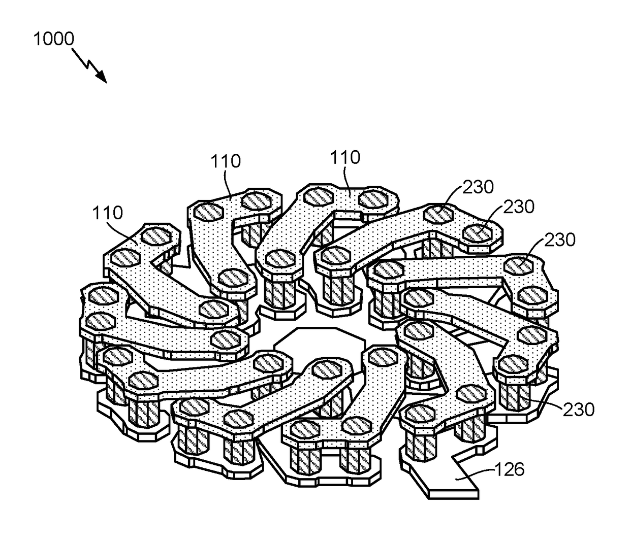
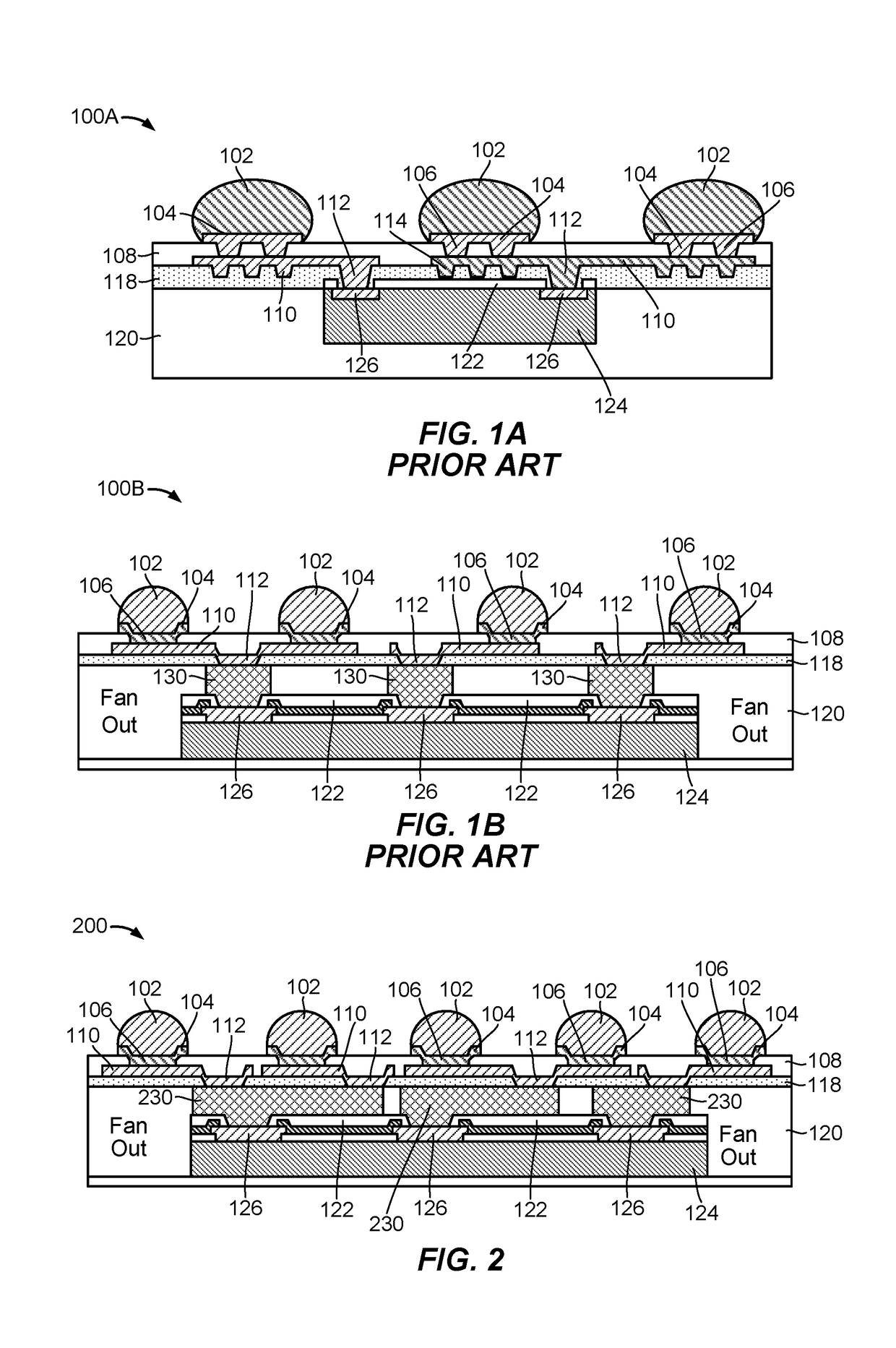
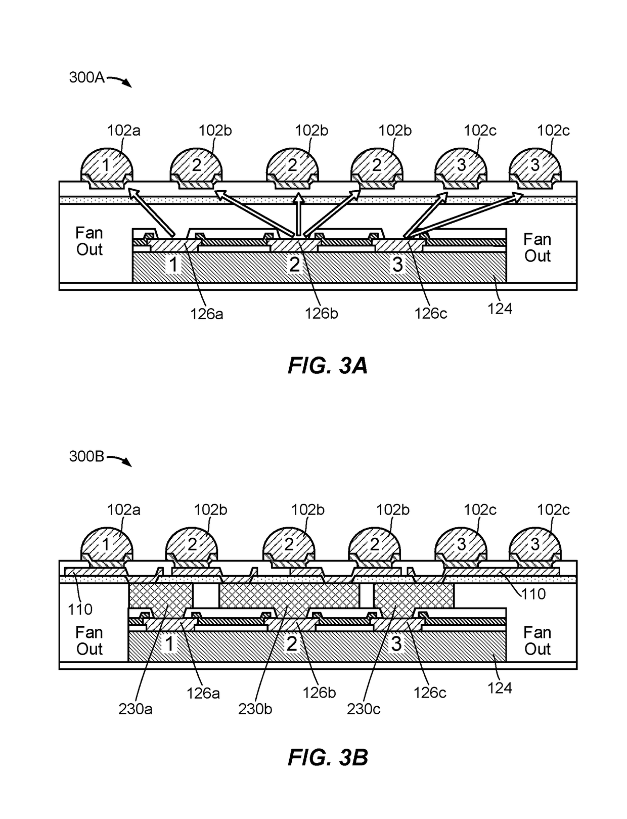
- Incorporating a second redistribution layer (RDL) with conductive pillars having a width-to-height ratio greater than one, allowing I/O connections to align with various package ball layouts without changing the layout of the semiconductor die's I/O connections, enabling flexible packaging without redesign.

Method for forming a redistribution layer in a wafer structure
PatentInactiveUS7420274B2
Innovation
- The redistribution layer is embedded within a passivation layer by forming grooves in a second passivation layer, where a seed layer is deposited on the sidewalls and filled with a metal material through electroplating, ensuring the redistribution layer is fixed tightly within the passivation layer to prevent delamination.


Supply Chain Considerations for Advanced Packaging
The supply chain landscape for advanced packaging technologies presents distinct challenges and opportunities when comparing Redistribution Layer (RDL) and Wafer Level Packaging (WLP) approaches. Each technology pathway requires different supplier ecosystems, manufacturing capabilities, and material sourcing strategies that significantly impact overall production feasibility and cost structures.
RDL-based packaging relies heavily on specialized substrate suppliers and advanced lithography equipment manufacturers. The supply chain typically involves high-end photoresist materials, specialized dielectric compounds, and precision metal deposition systems. Key suppliers include major chemical companies for advanced polymers and metallization materials, while equipment vendors must provide sophisticated lithography and etching capabilities. This creates dependencies on a relatively concentrated supplier base, potentially leading to supply chain vulnerabilities but also enabling deeper technical partnerships.
WLP supply chains demonstrate greater integration with traditional semiconductor manufacturing infrastructure. The technology leverages existing wafer fabrication facilities and established supplier relationships for silicon processing materials. This approach benefits from mature supply chains for wafer handling, dicing equipment, and standard semiconductor materials. However, WLP requires specialized bumping materials and underfill compounds that may involve different supplier networks than traditional IC manufacturing.
Geographic distribution of supply chain capabilities varies significantly between these approaches. RDL manufacturing tends to concentrate in regions with advanced packaging expertise, particularly in Asia-Pacific locations where major OSATs (Outsourced Semiconductor Assembly and Test) companies have established specialized facilities. WLP supply chains often align more closely with traditional semiconductor manufacturing hubs, leveraging existing wafer fab infrastructure and associated supplier networks.
Material availability and sourcing flexibility represent critical differentiators. RDL technologies often require specialized materials with longer lead times and higher minimum order quantities, potentially creating inventory management challenges. WLP approaches typically utilize more standardized materials with established supply chains, offering greater sourcing flexibility and shorter procurement cycles.
Risk mitigation strategies must account for these supply chain differences. RDL implementations may require dual sourcing for critical specialty materials and closer supplier partnerships to ensure technology roadmap alignment. WLP approaches can leverage more diversified supplier bases but must manage integration complexities across multiple technology domains.
Cost implications extend beyond material pricing to include supplier qualification expenses, inventory carrying costs, and supply chain management overhead. RDL supply chains may involve higher per-unit material costs but potentially lower qualification expenses due to fewer suppliers. WLP approaches might achieve better material pricing through established supply relationships while requiring more complex supplier management processes.
RDL-based packaging relies heavily on specialized substrate suppliers and advanced lithography equipment manufacturers. The supply chain typically involves high-end photoresist materials, specialized dielectric compounds, and precision metal deposition systems. Key suppliers include major chemical companies for advanced polymers and metallization materials, while equipment vendors must provide sophisticated lithography and etching capabilities. This creates dependencies on a relatively concentrated supplier base, potentially leading to supply chain vulnerabilities but also enabling deeper technical partnerships.
WLP supply chains demonstrate greater integration with traditional semiconductor manufacturing infrastructure. The technology leverages existing wafer fabrication facilities and established supplier relationships for silicon processing materials. This approach benefits from mature supply chains for wafer handling, dicing equipment, and standard semiconductor materials. However, WLP requires specialized bumping materials and underfill compounds that may involve different supplier networks than traditional IC manufacturing.
Geographic distribution of supply chain capabilities varies significantly between these approaches. RDL manufacturing tends to concentrate in regions with advanced packaging expertise, particularly in Asia-Pacific locations where major OSATs (Outsourced Semiconductor Assembly and Test) companies have established specialized facilities. WLP supply chains often align more closely with traditional semiconductor manufacturing hubs, leveraging existing wafer fab infrastructure and associated supplier networks.
Material availability and sourcing flexibility represent critical differentiators. RDL technologies often require specialized materials with longer lead times and higher minimum order quantities, potentially creating inventory management challenges. WLP approaches typically utilize more standardized materials with established supply chains, offering greater sourcing flexibility and shorter procurement cycles.
Risk mitigation strategies must account for these supply chain differences. RDL implementations may require dual sourcing for critical specialty materials and closer supplier partnerships to ensure technology roadmap alignment. WLP approaches can leverage more diversified supplier bases but must manage integration complexities across multiple technology domains.
Cost implications extend beyond material pricing to include supplier qualification expenses, inventory carrying costs, and supply chain management overhead. RDL supply chains may involve higher per-unit material costs but potentially lower qualification expenses due to fewer suppliers. WLP approaches might achieve better material pricing through established supply relationships while requiring more complex supplier management processes.
Cost-Performance Trade-offs in RDL vs WLP Selection
The selection between Redistribution Layer (RDL) and Wafer Level Packaging (WLP) technologies fundamentally revolves around balancing cost constraints with performance requirements. This decision-making process requires careful evaluation of multiple economic and technical factors that directly impact product viability and market competitiveness.
From a cost perspective, RDL technology typically presents higher initial investment requirements due to sophisticated lithography equipment and specialized materials. The manufacturing process involves multiple metal layers and dielectric depositions, resulting in increased processing time and material consumption. However, RDL offers superior routing flexibility and can accommodate complex interconnect patterns, potentially reducing the need for additional packaging layers and external components.
WLP technology generally provides more cost-effective solutions for high-volume production scenarios. The simplified process flow and reduced material requirements translate to lower per-unit manufacturing costs. Additionally, WLP's inherent miniaturization capabilities eliminate the need for traditional packaging substrates, further reducing overall system costs. However, the technology faces limitations in handling complex routing requirements and high pin-count applications.
Performance considerations significantly influence the cost-performance equation. RDL technology delivers superior electrical performance through optimized signal integrity, reduced parasitic effects, and enhanced thermal management capabilities. These performance advantages often justify higher costs in applications requiring stringent electrical specifications, such as high-frequency communications and advanced computing systems.
The scalability factor plays a crucial role in cost-performance trade-offs. While WLP demonstrates excellent cost efficiency in high-volume consumer electronics, RDL technology shows better cost-performance ratios in specialized applications where performance premiums outweigh manufacturing costs. Market segments demanding ultra-miniaturization with high performance typically favor RDL despite higher costs.
Manufacturing yield considerations further complicate the cost-performance analysis. RDL's complex processing steps may result in lower yields initially, increasing effective costs. Conversely, WLP's mature process technology often achieves higher yields, improving cost-effectiveness. The learning curve and process optimization timeline significantly impact the long-term cost-performance relationship for both technologies.
From a cost perspective, RDL technology typically presents higher initial investment requirements due to sophisticated lithography equipment and specialized materials. The manufacturing process involves multiple metal layers and dielectric depositions, resulting in increased processing time and material consumption. However, RDL offers superior routing flexibility and can accommodate complex interconnect patterns, potentially reducing the need for additional packaging layers and external components.
WLP technology generally provides more cost-effective solutions for high-volume production scenarios. The simplified process flow and reduced material requirements translate to lower per-unit manufacturing costs. Additionally, WLP's inherent miniaturization capabilities eliminate the need for traditional packaging substrates, further reducing overall system costs. However, the technology faces limitations in handling complex routing requirements and high pin-count applications.
Performance considerations significantly influence the cost-performance equation. RDL technology delivers superior electrical performance through optimized signal integrity, reduced parasitic effects, and enhanced thermal management capabilities. These performance advantages often justify higher costs in applications requiring stringent electrical specifications, such as high-frequency communications and advanced computing systems.
The scalability factor plays a crucial role in cost-performance trade-offs. While WLP demonstrates excellent cost efficiency in high-volume consumer electronics, RDL technology shows better cost-performance ratios in specialized applications where performance premiums outweigh manufacturing costs. Market segments demanding ultra-miniaturization with high performance typically favor RDL despite higher costs.
Manufacturing yield considerations further complicate the cost-performance analysis. RDL's complex processing steps may result in lower yields initially, increasing effective costs. Conversely, WLP's mature process technology often achieves higher yields, improving cost-effectiveness. The learning curve and process optimization timeline significantly impact the long-term cost-performance relationship for both technologies.
Unlock deeper insights with PatSnap Eureka Quick Research — get a full tech report to explore trends and direct your research. Try now!
Generate Your Research Report Instantly with AI Agent
Supercharge your innovation with PatSnap Eureka AI Agent Platform!