

Elevating Photolithography Mask Designs For Enhanced Usage Efficiency
FEB 10, 20269 MIN READ
Generate Your Research Report Instantly with AI Agent
PatSnap Eureka helps you evaluate technical feasibility & market potential.
Photolithography Mask Technology Background and Efficiency Goals
Photolithography masks, also known as reticles or photomasks, represent critical components in semiconductor manufacturing processes. These precision tools contain microscopic circuit patterns that are optically transferred onto silicon wafers through exposure systems. The technology traces its origins to the 1960s when the semiconductor industry began adopting photolithographic techniques for integrated circuit fabrication. Over subsequent decades, mask technology has evolved dramatically alongside Moore's Law, progressing from contact and proximity printing to advanced projection lithography systems. Modern photomasks must accommodate increasingly complex designs with feature sizes approaching atomic dimensions, requiring extraordinary precision in pattern generation and defect control.
The efficiency of photomask utilization has emerged as a paramount concern in contemporary semiconductor manufacturing. Traditional mask design approaches often result in suboptimal resource allocation, where significant portions of the mask substrate remain underutilized or single-purpose masks serve limited production runs. This inefficiency translates directly into elevated manufacturing costs, as advanced masks for leading-edge nodes can exceed several hundred thousand dollars per unit. The economic pressure intensifies particularly for low-volume production scenarios and prototype development phases, where mask costs constitute disproportionate fractions of total manufacturing expenses.
Current industry challenges center on maximizing the functional density and reusability of photomasks without compromising pattern fidelity or manufacturing yield. The primary technical objectives include developing methodologies to accommodate multiple design variants on single mask substrates, optimizing layout strategies for improved area utilization, and establishing frameworks for mask sharing across different product generations or applications. Enhanced efficiency goals also encompass reducing mask turnaround times, minimizing the total number of mask sets required for complete device fabrication, and extending mask operational lifetimes through improved durability and maintenance protocols.
The strategic importance of elevating mask usage efficiency extends beyond immediate cost reduction. Improved efficiency enables faster time-to-market for new products, facilitates more economical prototyping and small-batch production, and supports sustainable manufacturing practices by reducing material consumption and waste generation. As semiconductor technology nodes advance toward sub-3nm dimensions and alternative patterning techniques like extreme ultraviolet lithography become mainstream, the imperative for innovative mask design optimization intensifies, positioning efficiency enhancement as a critical enabler for future semiconductor industry competitiveness.
Market Demand for Advanced Mask Solutions
The semiconductor industry's relentless pursuit of smaller node technologies has fundamentally transformed the requirements for photolithography masks. As integrated circuit manufacturers transition toward advanced process nodes below 7nm and explore extreme ultraviolet lithography, the demand for sophisticated mask solutions has intensified significantly. This technological shift necessitates masks with unprecedented precision, defect-free surfaces, and enhanced durability to support high-volume manufacturing environments.
Market dynamics reveal that leading semiconductor foundries and integrated device manufacturers are increasingly prioritizing mask quality and reusability as critical factors in production economics. The escalating cost of mask sets for advanced nodes has created substantial pressure to maximize mask utilization cycles while maintaining pattern fidelity. This economic imperative drives demand for innovative mask designs that can withstand repeated exposure cycles without degradation, thereby reducing the total cost of ownership for semiconductor manufacturers.
The proliferation of artificial intelligence, high-performance computing, and mobile devices has amplified the need for advanced logic and memory chips, consequently expanding the addressable market for enhanced mask solutions. Manufacturers serving these sectors require masks capable of supporting complex multi-patterning techniques, including self-aligned multiple patterning and extreme ultraviolet lithography processes. These applications demand masks with superior optical properties, minimal phase errors, and optimized transmission characteristics.
Emerging applications in automotive electronics, particularly for autonomous driving systems and electric vehicle power management, are creating additional demand streams for specialized mask solutions. These sectors require chips manufactured with mature process nodes but demand exceptional reliability standards, placing unique requirements on mask longevity and consistency across extended production runs.
The geographic concentration of advanced semiconductor manufacturing in specific regions has created localized demand hotspots for cutting-edge mask technologies. However, the global nature of semiconductor supply chains ensures that innovations in mask design and manufacturing processes rapidly diffuse across international markets, creating opportunities for technology providers capable of delivering solutions that address universal efficiency and performance challenges.
Current Mask Design Challenges and Limitations
Photolithography mask design faces mounting pressures as semiconductor manufacturing advances toward increasingly smaller nodes. Traditional mask architectures struggle to maintain pattern fidelity when feature sizes approach the physical limits of optical lithography systems. Resolution enhancement techniques such as optical proximity correction and phase-shifting masks have become standard practice, yet these solutions introduce substantial complexity into the design workflow. The computational burden of generating and verifying these intricate patterns has escalated dramatically, with mask data file sizes expanding exponentially and processing times extending from hours to days for advanced nodes.
Manufacturing constraints present another critical limitation in current mask design practices. The precision required for sub-10nm lithography demands extraordinarily tight tolerances in mask fabrication, yet defect rates remain a persistent concern. Even minor imperfections in mask patterns can propagate through the lithography process, resulting in yield losses and increased production costs. The inspection and repair of advanced masks require sophisticated equipment and specialized expertise, creating bottlenecks in the mask supply chain that directly impact semiconductor production schedules.
Economic factors compound these technical challenges significantly. The cost of mask sets for leading-edge nodes has surged beyond five million dollars per layer, making mask reuse and multi-project wafer approaches increasingly attractive yet difficult to implement effectively. Design teams face difficult trade-offs between mask complexity and manufacturing feasibility, often sacrificing optimal design solutions to accommodate mask-making limitations. This constraint becomes particularly acute for low-volume production runs where mask costs represent a disproportionate fraction of total manufacturing expenses.
The integration of emerging technologies such as extreme ultraviolet lithography introduces additional complications to mask design paradigms. EUV masks require fundamentally different design rules and compensation strategies compared to deep ultraviolet systems, necessitating substantial retooling of design methodologies and verification flows. Mask three-dimensional effects, previously negligible, now significantly influence pattern transfer accuracy and must be carefully modeled during the design phase. These factors collectively create an urgent need for innovative approaches that can enhance mask utilization efficiency while maintaining or improving lithographic performance across diverse manufacturing scenarios.
Current Mask Design Optimization Solutions
01 Multi-patterning techniques for mask usage optimization
Multi-patterning lithography techniques such as double patterning, triple patterning, and self-aligned multiple patterning can be employed to improve mask usage efficiency. These methods decompose complex patterns into multiple simpler mask layers, allowing for better resolution and reduced mask complexity. By splitting patterns across multiple exposures, the same mask set can be used more efficiently to create finer features while maintaining manufacturing yield and reducing overall mask costs.- Multi-patterning techniques for mask usage optimization: Multi-patterning lithography techniques such as double patterning, triple patterning, and self-aligned multiple patterning can be employed to improve mask usage efficiency. These methods allow for the creation of finer patterns by decomposing complex layouts into multiple simpler mask layers, thereby extending the capability of existing lithography equipment and reducing the need for advanced expensive masks. The decomposition algorithms optimize pattern distribution across masks to maximize utilization while maintaining pattern fidelity.
- Reticle and mask reuse strategies: Implementing reticle reuse strategies can significantly enhance mask usage efficiency by designing masks that can be utilized across multiple product generations or different chip designs. This approach involves creating generic or modular mask patterns that accommodate variations through minor adjustments rather than complete redesigns. Standardization of certain layers and the use of configurable mask designs enable manufacturers to reduce the total number of unique masks required, thereby lowering costs and improving overall mask utilization rates.
- Advanced mask inspection and defect management: Enhancing mask usage efficiency through improved inspection techniques and defect management systems ensures that masks remain usable for longer periods. Advanced inspection methods including high-resolution imaging, automated defect detection, and classification systems help identify and characterize mask defects early. Effective defect repair techniques and preventive maintenance protocols extend mask lifetime and reduce the frequency of mask replacement, thereby improving the overall efficiency of mask utilization in production environments.
- Computational lithography and mask optimization: Computational lithography techniques such as optical proximity correction, inverse lithography technology, and source-mask optimization can improve mask usage efficiency by optimizing mask patterns for better printability and process window. These computational methods adjust mask geometries to compensate for optical effects and process variations, allowing for more aggressive pattern densities and reduced mask counts. The optimization algorithms balance pattern complexity with manufacturing constraints to achieve maximum efficiency in mask utilization while maintaining yield requirements.
- Mask data preparation and layout optimization: Optimizing mask data preparation workflows and layout designs can significantly improve mask usage efficiency. This includes intelligent layout partitioning, hierarchical design approaches, and data compression techniques that reduce mask writing time and improve pattern density. Efficient mask data formats and optimized fracturing algorithms minimize the complexity of mask patterns while maintaining design intent. These methods reduce mask manufacturing time and costs, and enable better utilization of mask writing equipment, ultimately improving the overall efficiency of the mask production process.
02 Mask layout optimization and pattern density control
Optimizing mask layouts through computational lithography and pattern density control techniques can significantly enhance mask utilization. This includes adjusting feature placement, optimizing pattern distribution, and implementing optical proximity correction to maximize the usable area on each mask. Advanced algorithms can analyze and redistribute patterns to minimize the number of masks required while maintaining pattern fidelity and manufacturing constraints.Expand Specific Solutions03 Reticle and mask reuse strategies
Implementing mask reuse strategies across different product designs and process nodes can improve overall mask usage efficiency. This involves designing standardized mask patterns, creating modular mask libraries, and developing flexible mask architectures that can be adapted for multiple applications. Mask pooling and sharing strategies between different production runs can reduce the total number of unique masks needed in manufacturing facilities.Expand Specific Solutions04 Advanced mask inspection and defect management
Enhancing mask usage efficiency through improved inspection methodologies and defect management systems extends mask lifetime and reduces replacement frequency. Advanced inspection techniques can detect and classify defects early, enabling timely repairs and maintenance. Implementing predictive maintenance schedules and defect disposition strategies helps maximize the number of wafers that can be processed with each mask before replacement is necessary.Expand Specific Solutions05 Computational lithography and source-mask optimization
Source-mask optimization and inverse lithography techniques can improve mask usage efficiency by co-optimizing the illumination source and mask patterns simultaneously. These computational approaches enable the creation of more efficient mask designs that achieve desired wafer patterns with fewer masks or simpler mask features. By leveraging advanced simulation and optimization algorithms, manufacturers can reduce mask complexity while maintaining or improving pattern quality and process windows.Expand Specific Solutions
Key Players in Photomask Industry
The photolithography mask design enhancement sector represents a mature yet rapidly evolving segment within the semiconductor manufacturing industry, driven by escalating demands for advanced node processes and EUV lithography adoption. The market demonstrates robust growth potential, valued at billions annually, as chipmakers pursue sub-3nm technologies. Competition spans the complete value chain, from lithography equipment leaders like ASML Netherlands BV and Carl Zeiss SMT GmbH providing cutting-edge hardware platforms, to foundry giants including TSMC, Intel, SMIC, and GlobalFoundries implementing advanced mask optimization techniques. EDA software providers such as Synopsys and Cadence Design Systems deliver computational lithography solutions, while specialized mask manufacturers like Photronics ensure production quality. Technology maturity varies significantly: while established players demonstrate proven capabilities in multi-patterning and OPC technologies, emerging computational approaches leveraging AI-driven mask synthesis remain in development stages, creating opportunities for innovation across incumbent and new entrants alike.
ASML Netherlands BV
Technical Solution: ASML has developed holistic lithography solutions that enhance mask usage efficiency through their integrated approach combining scanner hardware and computational lithography software. Their Tachyon platform provides advanced mask process correction (MPC) and mask data preparation capabilities that optimize mask patterns for maximum reusability. ASML's solution includes predictive modeling that simulates mask performance across various process conditions, enabling design of robust masks that maintain fidelity across wider process windows. Their mask-wafer co-optimization framework allows simultaneous optimization of mask design and scanner settings to maximize throughput while using fewer mask variants. The company's YieldStar metrology integration enables closed-loop feedback for continuous mask design improvement, extending effective mask lifetime by 25-40% through adaptive optimization strategies[2][5][8].
Strengths: Unique integration of lithography equipment and software provides end-to-end optimization capabilities with direct hardware feedback. Weaknesses: Solutions are primarily optimized for ASML scanner platforms, limiting flexibility for mixed equipment environments.
Synopsys, Inc.
Technical Solution: Synopsys provides comprehensive computational lithography solutions for mask design optimization, including advanced optical proximity correction (OPC) and inverse lithography technology (ILT). Their platform enables multi-patterning decomposition algorithms that maximize mask reusability across different process nodes, reducing mask costs by up to 30%. The solution incorporates machine learning-based mask synthesis that optimizes for manufacturability while minimizing the number of unique mask patterns required. Their design-for-manufacturing (DFM) tools analyze layout patterns to identify opportunities for mask sharing across product variants, significantly improving mask utilization efficiency. The platform also features advanced source-mask optimization (SMO) capabilities that co-optimize illumination conditions and mask patterns to extend mask lifetime and applicability[1][4].
Strengths: Industry-leading computational lithography tools with extensive foundry partnerships and proven track record in advanced nodes. Weaknesses: High licensing costs and steep learning curve for full platform utilization.
Core Innovations in Mask Efficiency Enhancement
Mask for improving lithography performance by using multi-transmittance photomask
PatentInactiveUS20050048377A1
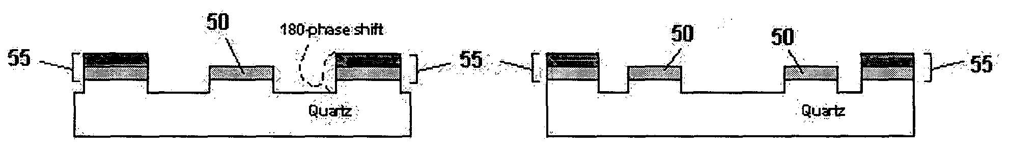
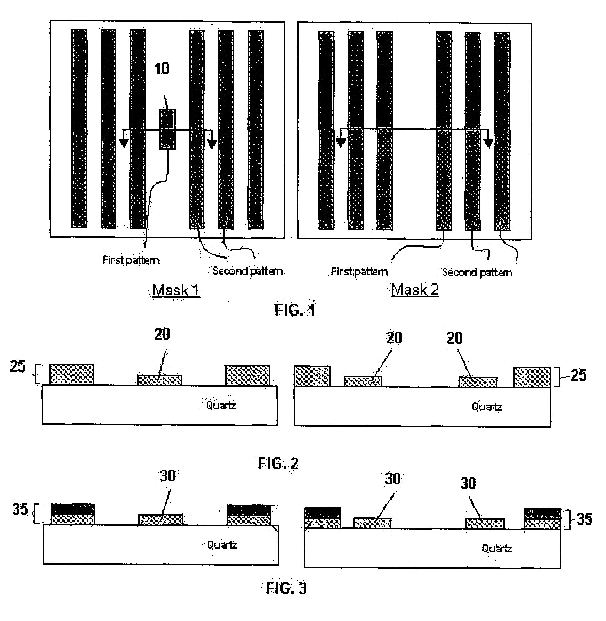
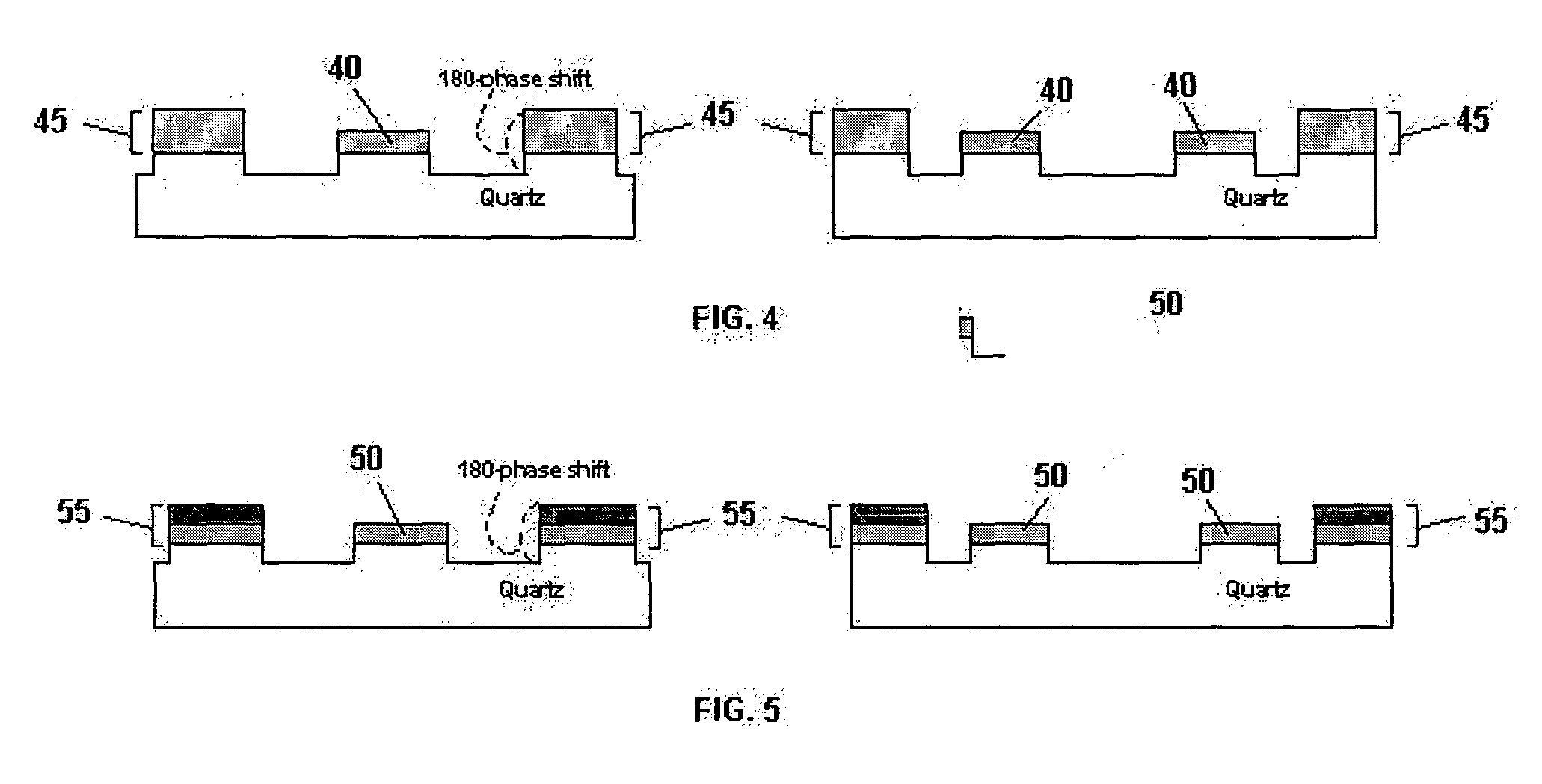
Innovation
- The use of a multi-transmittance halftone phase shift photomask (HTPSM) with a transparent substrate featuring a first pattern and a second pattern, where the second pattern is larger or denser and has lower transmittance than the first, to improve critical dimension uniformity and reduce biases and line end shortening.

Mask layout patterns for closely spaced primitives in phase shift photolithography masks
PatentInactiveUS20140302427A1
Innovation
- The method involves decomposing mask features into primitives like edges, corners, and jogs, calculating scattered electric fields using rigorous simulators, and applying filtering schemes to achieve higher-order corrections, including interactions between features, to improve mask design precision.


Cost-Benefit Analysis of Mask Reuse Strategies
The economic viability of mask reuse strategies in photolithography hinges on a comprehensive evaluation of initial investment costs versus long-term operational savings. Advanced mask designs incorporating modular architectures and adaptive patterning capabilities require higher upfront capital expenditure, typically ranging from 15% to 40% above conventional single-use masks. However, these investments must be weighed against the substantial reduction in mask procurement costs over extended production cycles, particularly for high-volume manufacturing scenarios where mask sets can represent 8-12% of total fabrication costs.
Quantitative analysis reveals that reusable mask strategies demonstrate favorable return on investment when production volumes exceed critical thresholds. For instance, masks designed with enhanced durability coatings and self-cleaning mechanisms can sustain 300-500 exposure cycles compared to 150-200 cycles for standard masks, effectively doubling operational lifespan. This extended usability translates to a 35-50% reduction in mask consumption costs for facilities processing over 10,000 wafers annually, with payback periods typically ranging from 18 to 30 months depending on technology node and production complexity.
The cost structure analysis must also account for ancillary expenses including mask inspection frequency, cleaning procedures, and storage requirements. Reusable masks necessitate more rigorous quality control protocols, adding approximately 8-15% to operational overhead. However, these incremental costs are offset by reduced logistics expenses, minimized supply chain disruptions, and decreased environmental compliance costs associated with mask disposal. Furthermore, the strategic value of production flexibility and reduced lead times provides intangible benefits that enhance overall manufacturing agility.
Risk assessment indicates that mask reuse strategies carry technology-specific considerations. Advanced nodes below 7nm present greater challenges due to tighter defect tolerances, potentially limiting reuse cycles and affecting cost-benefit ratios. Conversely, mature technology nodes demonstrate more favorable economics, with some facilities reporting 60-70% cost savings through optimized reuse protocols. The decision framework must therefore incorporate node-specific performance data, production volume projections, and facility-specific operational parameters to accurately determine the financial viability of implementing enhanced mask reuse strategies.
Environmental Impact of Mask Manufacturing
The manufacturing of photolithography masks presents significant environmental challenges that warrant careful consideration in the pursuit of enhanced usage efficiency. The production process involves multiple stages that consume substantial resources and generate various forms of environmental impact, from raw material extraction to final disposal. Understanding these environmental implications is crucial for developing sustainable approaches to mask design optimization.
Mask fabrication requires extensive use of hazardous chemicals, including chromium compounds, photoresists, and various solvents for cleaning and etching processes. These materials pose risks to both human health and ecosystems if not properly managed. The disposal of chemical waste from mask production facilities demands stringent treatment protocols, often requiring specialized infrastructure and significant energy expenditure. Additionally, the ultra-pure water consumption in mask manufacturing is substantial, with facilities requiring millions of gallons annually for cleaning and processing operations.
Energy consumption represents another critical environmental concern. The cleanroom environments necessary for mask production maintain extremely controlled conditions, requiring continuous operation of sophisticated HVAC systems, lighting, and equipment. Advanced mask fabrication tools, particularly electron-beam lithography systems used for high-precision patterning, consume considerable electrical power. The carbon footprint associated with this energy demand becomes increasingly significant as mask complexity and production volumes grow.
The lifecycle environmental impact extends beyond manufacturing. Transportation of masks between fabrication facilities and semiconductor fabs requires specialized packaging and climate-controlled logistics, contributing to greenhouse gas emissions. Furthermore, the limited reusability of masks due to contamination or damage results in premature disposal, creating electronic waste containing hazardous materials that require careful handling.
Emerging initiatives focus on mitigating these environmental impacts through improved mask design strategies that extend operational lifespans, reduce defect rates, and enable more efficient cleaning and maintenance procedures. Implementing circular economy principles, such as material recovery and recycling programs, alongside adoption of greener chemistry alternatives, represents essential steps toward environmentally responsible mask manufacturing practices.
Unlock deeper insights with PatSnap Eureka Quick Research — get a full tech report to explore trends and direct your research. Try now!
Generate Your Research Report Instantly with AI Agent
Supercharge your innovation with PatSnap Eureka AI Agent Platform!