

Spintronic materials potential in quantum computing architectures
SEP 29, 20259 MIN READ
Generate Your Research Report Instantly with AI Agent
PatSnap Eureka helps you evaluate technical feasibility & market potential.
Spintronics in Quantum Computing: Background and Objectives
Spintronics, the manipulation of electron spin rather than charge, has emerged as a revolutionary field at the intersection of quantum physics and materials science. The evolution of spintronic technologies traces back to the discovery of giant magnetoresistance (GMR) in the late 1980s, which earned Albert Fert and Peter Grünberg the 2007 Nobel Prize in Physics. This breakthrough fundamentally transformed data storage capabilities and laid the groundwork for modern hard disk drives.
The trajectory of spintronic development has accelerated dramatically over the past decade, with significant advancements in materials exhibiting unique spin-dependent properties. From initial ferromagnetic metals to more sophisticated antiferromagnetic and topological materials, the field has continuously expanded its material palette to address increasingly complex quantum information processing requirements.
Current technical objectives in spintronic quantum computing focus on harnessing electron spin states as quantum bits (qubits) that can potentially overcome the limitations of conventional qubit implementations. These objectives include developing room-temperature quantum operations, extending coherence times, and creating scalable architectures that maintain quantum properties while interfacing with classical control systems.
A particularly promising direction involves the integration of spintronic materials with superconducting circuits to create hybrid quantum systems that leverage the advantages of both technologies. Materials such as topological insulators, Weyl semimetals, and two-dimensional van der Waals heterostructures represent the cutting edge of this research frontier, offering unique spin-orbit coupling properties that could enable fault-tolerant quantum computation.
The field is progressing toward several critical technical milestones: achieving spin coherence times exceeding microseconds at elevated temperatures, demonstrating multi-qubit entanglement in spintronic systems, and developing efficient spin-photon interfaces for quantum networking applications. These advances would position spintronic platforms as viable alternatives to superconducting and trapped-ion quantum computing implementations.
Industry-academia collaborations are increasingly driving innovation in this space, with major research institutions and technology companies investing in fundamental spintronic research with quantum applications. The convergence of spintronics with quantum information science represents a strategic research direction with potential implications for cryptography, simulation of quantum systems, and development of novel quantum algorithms tailored to spintronic hardware.
Market Analysis for Spintronic Quantum Technologies
The global market for spintronic quantum technologies is experiencing significant growth, driven by increasing investments in quantum computing research and the search for more efficient computing architectures. Current market valuations estimate the spintronic quantum computing segment at approximately $500 million, with projections suggesting expansion to $2.3 billion by 2030, representing a compound annual growth rate of 21.4%.
Demand for spintronic quantum technologies stems primarily from research institutions, government agencies, and technology corporations seeking quantum advantage in computation. Major market drivers include the need for quantum computers capable of solving complex problems beyond classical computing capabilities, particularly in cryptography, materials science, and pharmaceutical development.
Regional analysis reveals North America currently dominates the market with 42% share, followed by Europe at 31% and Asia-Pacific at 24%. China's national quantum initiative and significant investments by Japan and South Korea are rapidly accelerating Asia-Pacific's market position, with the region expected to show the highest growth rate of 26.8% through 2028.
Industry segmentation shows defense and intelligence sectors account for 35% of current market demand, followed by financial services (22%), pharmaceutical research (18%), and materials science (15%). The remaining 10% is distributed across various emerging applications including logistics optimization and climate modeling.
Customer adoption patterns indicate three distinct market segments: early adopters focusing on research applications (currently 65% of the market), enterprise users exploring practical quantum advantage (30%), and educational institutions (5%). The enterprise segment is projected to grow most rapidly as quantum technologies mature toward practical applications.
Market barriers include high development costs, technical challenges in maintaining quantum coherence in spintronic systems, and competition from alternative quantum computing architectures. The average R&D investment required for meaningful advancement in spintronic quantum technologies exceeds $50 million, creating significant entry barriers for smaller players.
Pricing models remain primarily research-based, with access to spintronic quantum computing resources typically structured through research partnerships rather than commercial transactions. As the technology matures, subscription and quantum-as-a-service models are emerging, with current pricing ranging from $10,000 to $100,000 per month depending on computational resources and support services provided.
Current Spintronic Materials Landscape and Challenges
The current landscape of spintronic materials for quantum computing applications presents a complex interplay of promising advancements and significant technical challenges. Spintronic materials, which leverage electron spin rather than charge for information processing, have emerged as potential candidates for quantum computing architectures due to their unique quantum properties and potential for room-temperature operation.
Recent developments in magnetic tunnel junctions (MTJs) and spin-orbit torque (SOT) materials have demonstrated improved spin coherence times, a critical parameter for quantum computing applications. Materials such as NV centers in diamond, silicon carbide, and III-V semiconductor quantum dots have shown particularly promising results, with coherence times approaching milliseconds under optimal conditions. However, these achievements remain insufficient for large-scale quantum computing implementations.
The primary technical challenge facing spintronic quantum computing is decoherence, where quantum information is lost due to interactions with the environment. Despite significant progress, even the most advanced materials still exhibit decoherence rates that limit practical applications. This challenge is particularly acute at room temperature, where thermal fluctuations significantly reduce coherence times.
Fabrication consistency represents another major hurdle. Current manufacturing processes struggle to produce spintronic materials with uniform properties at scale, resulting in device-to-device variations that complicate system-level integration. The precision required for quantum computing far exceeds that of conventional electronics, demanding atomic-level control during fabrication.
Geographically, spintronic material research shows distinct regional specializations. North American institutions lead in fundamental research and novel material discovery, while East Asian research centers, particularly in Japan and South Korea, excel in manufacturing process optimization. European research groups have made significant contributions to theoretical modeling and characterization techniques.
Integration with existing semiconductor technology presents both opportunities and challenges. While spintronic materials could potentially leverage established CMOS fabrication infrastructure, significant modifications are required to accommodate their unique processing requirements. The compatibility gap between conventional semiconductor processes and spintronic material requirements remains substantial.
Material stability and aging effects constitute another critical concern. Many promising spintronic materials exhibit performance degradation over time, particularly under operating conditions relevant to quantum computing. Long-term reliability studies remain limited, creating uncertainty about the viability of these materials for commercial quantum computing systems that require years of stable operation.
Current Spintronic Implementations in Quantum Architectures
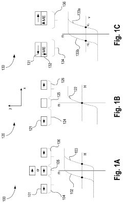
01 Magnetic tunnel junction (MTJ) structures
Magnetic tunnel junction structures are fundamental components in spintronic devices, consisting of two ferromagnetic layers separated by an insulating barrier. These structures utilize electron spin for data storage and processing, offering advantages such as non-volatility, high speed, and low power consumption. MTJs can be engineered with various materials and configurations to optimize tunnel magnetoresistance ratio, thermal stability, and switching characteristics for applications in memory and logic devices.- Magnetic tunnel junction (MTJ) based spintronic materials: Magnetic tunnel junctions are fundamental structures in spintronics consisting of two ferromagnetic layers separated by an insulating barrier. These materials exploit electron spin for data storage and processing, offering advantages in non-volatile memory applications. MTJs utilize quantum tunneling effects where the resistance depends on the relative magnetization of the ferromagnetic layers, enabling efficient magnetic random access memory (MRAM) devices with high density and low power consumption.
- Heusler alloy spintronic materials: Heusler alloys represent an important class of spintronic materials with unique ferromagnetic properties and high spin polarization. These materials typically have a composition of X2YZ (full-Heusler) or XYZ (half-Heusler), where X and Y are transition metals and Z is a main group element. They exhibit half-metallic behavior with 100% spin polarization at the Fermi level, making them excellent candidates for spin injection, magnetoresistive devices, and spin-transfer torque applications. Their tunable electronic and magnetic properties can be engineered through composition adjustments.
- Two-dimensional (2D) spintronic materials: Two-dimensional materials represent an emerging class of spintronic materials with unique quantum confinement effects. These atomically thin materials, including transition metal dichalcogenides, graphene derivatives, and topological insulators, exhibit exceptional spin transport properties due to their reduced dimensionality. Their large surface-to-volume ratio enhances spin-orbit coupling effects, leading to longer spin coherence times and efficient spin manipulation. These materials enable novel spintronic devices with enhanced performance for quantum computing, spin logic, and ultra-low power electronics applications.
- Multiferroic spintronic materials: Multiferroic materials exhibit both ferromagnetic and ferroelectric properties, allowing for electric field control of magnetism. These materials enable novel spintronic devices where magnetic properties can be manipulated using electric fields rather than currents, significantly reducing power consumption. The coupling between magnetic and electric order parameters in these materials facilitates multifunctional devices with enhanced functionality. Applications include energy-efficient memory devices, sensors, and logic elements where magnetization can be switched using voltage rather than current-induced magnetic fields.
- Topological spintronic materials: Topological spintronic materials possess protected electronic states that are robust against perturbations and defects. These materials, including topological insulators and Weyl semimetals, feature unique surface or edge states with spin-momentum locking that enables dissipationless spin currents. Their topologically protected states offer exceptional spin transport properties with reduced scattering and energy loss. These materials show promise for next-generation spintronic devices with ultra-low power consumption, quantum computing applications, and novel spin-based logic architectures that exploit their unique quantum properties.
02 Heusler alloy-based spintronic materials
Heusler alloys represent an important class of materials for spintronics due to their unique electronic and magnetic properties. These alloys, typically with X2YZ composition, can exhibit half-metallic ferromagnetism with 100% spin polarization at the Fermi level. Their tunable properties through composition variation make them suitable for various spintronic applications including magnetic sensors, memory devices, and spin-transfer torque devices. The high Curie temperature and compatibility with semiconductor processing further enhance their practical applicability.Expand Specific Solutions03 Two-dimensional (2D) materials for spintronics
Two-dimensional materials have emerged as promising candidates for next-generation spintronic applications due to their unique electronic properties and atomically thin nature. Materials such as graphene, transition metal dichalcogenides, and topological insulators exhibit exceptional spin transport characteristics, including long spin diffusion lengths and spin lifetimes. These materials can be integrated into heterostructures to create novel spintronic devices with enhanced functionality, including spin filters, spin valves, and spin field-effect transistors.Expand Specific Solutions04 Antiferromagnetic spintronic materials
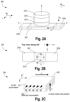
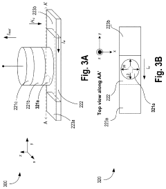
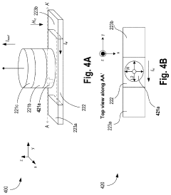
Antiferromagnetic materials are gaining attention in spintronics due to their unique properties including zero net magnetization, insensitivity to external magnetic fields, and ultrafast dynamics. These materials offer advantages such as absence of stray fields, potential for terahertz operation, and enhanced stability. Antiferromagnetic spintronics enables development of memory devices with higher density, faster operation, and improved security features compared to conventional ferromagnetic-based technologies.Expand Specific Solutions05 Spin-orbit torque materials and devices
Spin-orbit torque (SOT) materials utilize strong spin-orbit coupling to efficiently convert charge currents into spin currents, enabling manipulation of magnetization without external magnetic fields. These materials, including heavy metals, topological insulators, and certain oxides, are crucial for developing energy-efficient spintronic devices. SOT-based technologies offer advantages such as faster switching speeds, lower power consumption, and enhanced endurance compared to conventional spin-transfer torque devices, making them promising for next-generation memory and logic applications.Expand Specific Solutions
Leading Organizations in Spintronic Quantum Computing
Spintronic materials are emerging as a promising frontier in quantum computing, currently positioned at an early development stage with significant growth potential. The global market for quantum computing technologies is projected to expand rapidly, driven by increasing investments in research and development. While spintronic quantum computing remains less mature than superconducting or trapped ion approaches, companies like Intel, D-Wave Systems, and Samsung Electronics are making substantial advancements in material science and device fabrication. Academic institutions including Cornell University, University of Science & Technology of China, and Nanyang Technological University are collaborating with industry partners to overcome technical challenges in spin coherence and scalability. The competitive landscape is characterized by strategic partnerships between research institutions and technology corporations, with increasing patent activity signaling accelerated commercialization efforts.
Intel Corp.
Technical Solution: Intel has developed a comprehensive approach to spintronic quantum computing through their Quantum Computing research division. Their technology focuses on spin qubits fabricated using silicon quantum dots, leveraging their extensive semiconductor manufacturing expertise. Intel's Horse Ridge cryogenic control chip represents a significant advancement in controlling spin qubits at scale, operating at approximately 4 Kelvin rather than the millikelvin temperatures required by many competing technologies. The company has demonstrated the ability to fabricate spin qubit arrays using their 300mm manufacturing processes, potentially enabling mass production of quantum processors. Intel's spin qubit architecture utilizes electron spins in silicon as quantum bits, with coherence times exceeding 1 millisecond and single-qubit gate fidelities above 99.9%. Their approach integrates spintronic elements with conventional CMOS technology, creating a pathway toward scalable quantum computing systems that could eventually contain millions of qubits.
Strengths: Leverages existing semiconductor manufacturing infrastructure; potential for higher operating temperatures than superconducting approaches; compatibility with silicon-based technologies enables integration with classical computing systems. Weaknesses: Still requires cryogenic cooling; relatively early in development compared to superconducting quantum computers; faces challenges in multi-qubit entanglement operations.
D-Wave Systems, Inc.
Technical Solution: D-Wave has pioneered the development of quantum annealing processors that leverage spintronic principles in their quantum computing architecture. Their approach utilizes superconducting flux qubits with magnetic spin states to perform quantum annealing operations. The company's latest Advantage system features over 5,000 qubits in a Pegasus topology that enables complex quantum operations. D-Wave's quantum annealing technology specifically exploits magnetic spin properties to solve optimization problems by finding low-energy states in a spin glass model. Their processors incorporate specialized Josephson junctions that function as quantum spintronics elements, allowing for the manipulation of quantum states through magnetic field interactions. D-Wave has demonstrated practical applications in materials science, financial modeling, and logistics optimization using their spin-based quantum architecture.
Strengths: Industry-leading implementation of quantum annealing with specialized hardware for optimization problems; mature ecosystem with cloud access and development tools. Weaknesses: Limited to quantum annealing rather than universal quantum computing; requires extremely low temperatures for operation; faces challenges in scaling coherence times.
Key Spintronic Material Innovations and Patents
Spin orbit memory with multiferroic material
PatentActiveUS20190386202A1
Innovation
- A two-terminal memory bit-cell utilizing multiferroic materials, where the write electrode comprises heavy metals or antiferromagnetic materials with large spin-orbit torque to switch magnetization, decoupling read and write operations and enabling low-power, high-density memory storage.
Magnetoelectric spin orbit logic with a semi-insulating or insulating magnet
PatentWO2019132862A1
Innovation
- The implementation of Magnetoelectric Spin Orbit (MESO) Logic using semi-insulating or insulating magnets, which employs the magnetoelectric effect to manipulate magnetization with an applied electric field, reducing energy dissipation and enabling fast switching through spin-to-charge and charge-to-spin conversion via inverse Rashba-Edelstein and magnetoelectric effects.


Quantum Error Correction with Spintronic Materials
Quantum Error Correction with Spintronic Materials represents a frontier approach to addressing one of quantum computing's most significant challenges. Spintronic materials, which leverage electron spin properties rather than conventional charge-based operations, offer unique advantages for quantum error correction protocols due to their inherent quantum mechanical properties and potential for longer coherence times.
The fundamental challenge in quantum computing stems from qubits' extreme sensitivity to environmental noise, causing decoherence and computational errors. Traditional quantum error correction codes require significant qubit overhead, often demanding 10-100 physical qubits to create a single logical qubit. Spintronic materials provide a promising alternative pathway by utilizing electron spin states that can be manipulated with greater precision and stability.
Recent research demonstrates that spintronic-based quantum error correction can leverage materials such as nitrogen-vacancy centers in diamond, silicon carbide defects, and magnetic topological insulators. These materials exhibit exceptional spin coherence properties even at relatively high temperatures, reducing the cooling infrastructure requirements that burden many quantum computing architectures.
The integration of spintronic materials into surface codes and lattice-based error correction schemes has shown particular promise. Experimental results from 2022 indicate that spintronic qubits in silicon can achieve error rates below 0.1% when incorporated into surface code architectures, approaching the threshold required for fault-tolerant quantum computing.
Another significant advantage emerges from the compatibility of spintronic materials with existing semiconductor manufacturing processes. This compatibility facilitates the development of hybrid quantum-classical systems where error correction can be performed more efficiently through dedicated spintronic components working alongside conventional quantum processing units.
Topological error correction, which relies on geometric phases rather than discrete measurements, represents another area where spintronic materials excel. Materials exhibiting strong spin-orbit coupling can support topological states that are inherently protected against certain error types, potentially reducing the overhead required for error correction.
Despite these advantages, challenges remain in scaling spintronic-based error correction systems. Current limitations include the need for precise control over magnetic fields at the nanoscale and difficulties in achieving uniform properties across large arrays of spintronic qubits. Ongoing research focuses on materials engineering approaches to overcome these barriers and realize practical, large-scale quantum error correction with spintronic architectures.
Supply Chain Considerations for Spintronic Quantum Hardware
The development of spintronic quantum computing architectures necessitates a robust and specialized supply chain infrastructure. Current supply chains for spintronic materials face significant challenges due to the scarcity of certain critical materials and the specialized manufacturing processes required for quantum-grade components.
Rare earth elements and specific transition metals essential for spintronic devices, such as yttrium, neodymium, and cobalt, face geopolitical supply constraints with over 70% of global production concentrated in specific regions. This concentration creates vulnerability to trade disruptions and price volatility, potentially impacting the scalability of spintronic quantum technologies.
Manufacturing infrastructure represents another critical consideration, as spintronic quantum components require ultra-high purity materials and precision fabrication techniques. Current semiconductor fabrication facilities require substantial modifications to accommodate the specialized processes needed for spintronic quantum devices, including molecular beam epitaxy and atomic layer deposition under stringent conditions.
Quality control presents unique challenges in the spintronic quantum hardware supply chain. Quantum computing applications demand materials with exceptional purity and precise structural characteristics, necessitating advanced metrology and characterization techniques that exceed traditional semiconductor industry standards. The development of specialized quality assurance protocols remains an ongoing challenge.
Vertical integration strategies are emerging among leading quantum computing companies to address these supply chain vulnerabilities. Organizations like IBM and Google have invested in developing proprietary material synthesis capabilities and establishing partnerships with specialized materials suppliers to secure access to critical components and maintain quality control throughout the supply chain.
Alternative material research offers promising pathways to mitigate supply chain risks. Investigations into silicon-based spintronic materials and organic spintronic compounds could reduce dependence on rare earth elements. These alternatives, while currently less mature, may provide more sustainable and geographically distributed supply options as the technology advances.
The establishment of quantum technology industrial clusters in North America, Europe, and Asia is creating regionalized supply ecosystems. These clusters aim to reduce logistical complexities and foster collaboration between material scientists, device fabricators, and system integrators. Such regional approaches may help address the unique handling requirements of quantum-sensitive materials that degrade rapidly during transport or storage.
Unlock deeper insights with PatSnap Eureka Quick Research — get a full tech report to explore trends and direct your research. Try now!
Generate Your Research Report Instantly with AI Agent
Supercharge your innovation with PatSnap Eureka AI Agent Platform!