

Spintronic materials surface modification and defect control research
SEP 29, 20259 MIN READ
Generate Your Research Report Instantly with AI Agent
PatSnap Eureka helps you evaluate technical feasibility & market potential.
Spintronics Background and Research Objectives
Spintronics represents a revolutionary field at the intersection of electronics and quantum mechanics, leveraging the intrinsic spin property of electrons rather than their charge for information processing and storage. Since its theoretical foundations in the 1980s and experimental breakthroughs in the 1990s with the discovery of giant magnetoresistance (GMR), spintronics has evolved from a purely academic pursuit to a cornerstone technology for next-generation computing and data storage solutions.
The evolution of spintronic materials has progressed through several generations, from simple ferromagnetic metals to complex multilayer heterostructures and, more recently, to topological materials and two-dimensional systems. Each advancement has expanded the potential applications while simultaneously introducing new challenges related to material quality, interface properties, and quantum coherence.
Surface modification and defect control represent critical frontiers in spintronic materials research. The performance of spintronic devices is extraordinarily sensitive to surface and interface conditions, as spin transport and manipulation primarily occur at these boundaries. Even minor defects or contamination can significantly disrupt spin coherence and transport efficiency, undermining device performance.
Current research objectives in this domain focus on developing precise methodologies for surface engineering that can enhance spin injection efficiency, prolong spin lifetime, and maintain quantum coherence across interfaces. This includes atomic-level control of surface termination, interface engineering between different materials, and strategic introduction of specific defects that may actually enhance desired spintronic properties.
Another key objective involves establishing standardized characterization techniques for spintronic material surfaces and defects. The quantum mechanical nature of spin phenomena necessitates advanced analytical methods that can probe magnetic, electronic, and structural properties simultaneously at nanoscale dimensions.
The long-term vision extends beyond incremental improvements to transformative capabilities. By mastering surface modification and defect control, researchers aim to develop room-temperature quantum spintronic devices with significantly reduced power consumption compared to conventional electronics. This could enable practical quantum computing architectures, ultra-sensitive magnetic sensors, and neuromorphic computing systems that mimic the brain's energy efficiency.
Achieving these objectives requires interdisciplinary collaboration spanning materials science, surface physics, quantum mechanics, and device engineering. The convergence of these fields promises to unlock new functionalities in spintronic systems while addressing fundamental challenges in quantum information processing and energy-efficient computing.
Market Analysis for Spintronic Applications
The global market for spintronic applications has witnessed substantial growth in recent years, driven primarily by increasing demand for high-density data storage solutions and energy-efficient electronic devices. The market value reached approximately $5.9 billion in 2022 and is projected to grow at a CAGR of 34.7% through 2030, potentially reaching $39.1 billion by the end of the forecast period.
Data storage remains the dominant application segment, accounting for nearly 65% of the total market share. This dominance stems from the widespread adoption of spintronic-based magnetic random access memory (MRAM) and spin-transfer torque MRAM (STT-MRAM) technologies in enterprise storage systems, automotive electronics, and industrial automation equipment.
The semiconductor industry represents the second-largest market segment, where spintronic materials with optimized surface properties and minimal defects are crucial for developing next-generation logic devices. This segment is expected to grow at the fastest rate, with a CAGR of 38.2% through 2030, driven by increasing investments in quantum computing and neuromorphic computing architectures.
Geographically, North America leads the market with approximately 38% share, followed by Asia-Pacific at 35% and Europe at 22%. However, the Asia-Pacific region is expected to witness the highest growth rate due to expanding semiconductor manufacturing capabilities in China, South Korea, and Taiwan, coupled with increasing government investments in advanced electronics research.
The automotive and aerospace sectors are emerging as promising application areas, particularly for sensors and non-volatile memory components that can withstand extreme operating conditions. Market penetration in these sectors is expected to accelerate as surface modification techniques improve the reliability and performance of spintronic materials under varying environmental conditions.
Consumer electronics represents another high-potential market, with smartphone manufacturers increasingly incorporating spintronic components to enhance energy efficiency and processing capabilities. This segment is projected to grow at a CAGR of 29.8% through 2030, creating significant opportunities for materials with optimized surface properties.
The market landscape is characterized by a growing emphasis on defect-free materials, as even minor imperfections can significantly impact device performance. Consequently, companies investing in advanced surface modification techniques and defect control methodologies are positioned to capture premium market segments where reliability and performance consistency are paramount.
Current Challenges in Surface Modification Techniques
Surface modification of spintronic materials faces significant technical challenges that impede the advancement of next-generation spintronic devices. The primary obstacle lies in achieving precise control over the interface properties at the atomic level. Current techniques such as molecular beam epitaxy (MBE) and pulsed laser deposition (PLD) struggle to maintain consistent quality across large surface areas, resulting in non-uniform magnetic properties that compromise device performance.
Contamination control represents another major hurdle in surface modification processes. Even trace amounts of oxygen or carbon can dramatically alter the spin-dependent transport properties at interfaces. Despite the implementation of ultra-high vacuum environments, achieving and maintaining contamination-free surfaces throughout the entire modification process remains problematic, particularly during transfers between processing chambers.
The characterization of modified surfaces presents its own set of challenges. While techniques such as X-ray photoelectron spectroscopy (XPS) and scanning tunneling microscopy (STM) provide valuable insights, they often cannot capture the dynamic behavior of spins at interfaces under operational conditions. This limitation creates a disconnect between laboratory characterization and actual device performance.
Defect control during surface modification introduces additional complexity. Point defects, dislocations, and grain boundaries significantly influence spin transport and magnetic anisotropy. Current methodologies lack the precision to systematically control these defects, leading to unpredictable variations in device performance. The trade-off between processing temperature and defect formation remains particularly problematic for temperature-sensitive spintronic materials.
Scalability issues further complicate industrial implementation of laboratory-proven techniques. Methods that work effectively for small research samples often encounter significant challenges when scaled to production-level wafers. The cost-effectiveness of precision techniques like atomic layer deposition becomes questionable at industrial scales, creating barriers to commercialization.
Integration compatibility with existing semiconductor manufacturing processes represents another significant challenge. Many effective surface modification techniques for spintronic materials require conditions incompatible with CMOS processing standards, limiting their practical application in integrated devices. The development of techniques that can seamlessly integrate with established manufacturing flows remains an ongoing challenge.
Finally, the long-term stability of modified surfaces under various operational conditions (temperature fluctuations, magnetic fields, electrical currents) remains inadequately addressed. Surface degradation over time can lead to performance drift in spintronic devices, raising reliability concerns for commercial applications. Current accelerated aging tests often fail to accurately predict real-world performance over extended periods.
State-of-the-Art Surface Modification Methods
01 Surface modification techniques for spintronic materials
Various surface modification techniques can be applied to spintronic materials to enhance their performance characteristics. These techniques include plasma treatment, chemical etching, and atomic layer deposition that can precisely control the surface properties. Surface modification helps in improving interface quality, which is critical for spin transport and magnetic coupling in spintronic devices. These methods can effectively reduce surface defects and create atomically smooth interfaces necessary for optimal spin-dependent transport.- Surface modification techniques for spintronic materials: Various surface modification techniques can be applied to spintronic materials to enhance their performance and functionality. These techniques include plasma treatment, chemical etching, and atomic layer deposition, which can modify the surface properties of spintronic materials. Surface modification helps in controlling the interface properties, which are crucial for spin transport and magnetic behavior in spintronic devices.
- Defect engineering in magnetic thin films: Defect engineering involves the controlled introduction or elimination of defects in magnetic thin films to manipulate their spintronic properties. Techniques such as ion implantation, thermal annealing, and strain engineering can be used to create or heal defects. These defects can significantly influence magnetic anisotropy, spin polarization, and magnetoresistance, which are essential properties for spintronic applications.
- Interface control for enhanced spin transport: Controlling the interface between different materials in spintronic devices is crucial for efficient spin transport. This can be achieved through precise deposition techniques, interface engineering, and the use of buffer layers. Clean interfaces with minimal defects and controlled roughness can significantly improve spin injection, transport, and detection, leading to better performance of spintronic devices.
- Nanoscale patterning and structuring of spintronic materials: Nanoscale patterning and structuring techniques can be applied to spintronic materials to create specific geometries and architectures that enhance their functional properties. These techniques include lithography, etching, and self-assembly methods. Controlled nanoscale structures can lead to novel spin-dependent phenomena and improved device performance through the manipulation of domain walls, spin waves, and magnetic configurations.
- Passivation and protection of spintronic surfaces: Passivation and protection techniques are essential for maintaining the integrity and performance of spintronic materials, especially under harsh environmental conditions. These techniques involve the application of protective layers, encapsulation, and surface treatments that prevent oxidation and degradation. Effective passivation can extend the lifetime of spintronic devices and ensure stable operation over time.
02 Defect engineering in magnetic thin films
Controlled introduction and manipulation of defects in magnetic thin films can significantly influence their spintronic properties. Techniques such as ion implantation, thermal annealing, and strain engineering are used to create and control defects like vacancies, interstitials, and grain boundaries. These defects can serve as pinning sites for magnetic domain walls or act as scattering centers for spin-polarized electrons. By precisely controlling the type, concentration, and distribution of defects, researchers can tailor the magnetic anisotropy, coercivity, and spin transport properties of spintronic materials.Expand Specific Solutions03 Interface engineering for enhanced spin transport
The quality of interfaces between different materials in spintronic devices critically affects spin transport efficiency. Interface engineering techniques involve precise control of atomic arrangements, chemical composition, and electronic structure at material boundaries. Methods such as molecular beam epitaxy, pulsed laser deposition, and sputtering with controlled parameters are employed to create atomically sharp interfaces. Reducing interface roughness and interdiffusion while optimizing band alignment can significantly enhance spin injection, transport, and detection efficiencies in spintronic devices.Expand Specific Solutions04 Nanoscale patterning and structuring of spintronic materials
Nanoscale patterning and structuring techniques are applied to spintronic materials to create specific geometries that enhance their functional properties. Methods such as electron beam lithography, nanoimprint lithography, and focused ion beam milling enable the creation of precisely defined structures at the nanoscale. These techniques allow for the fabrication of nanopillars, nanowires, and nanodots with controlled dimensions and spacing. Such nanostructured spintronic materials exhibit unique magnetic properties due to confinement effects and can be used to create high-density magnetic storage devices and novel spintronic circuit elements.Expand Specific Solutions05 Passivation and protection strategies for spintronic devices
Passivation and protection strategies are essential for maintaining the performance and extending the lifetime of spintronic devices. These include the application of capping layers, encapsulation techniques, and surface treatments that prevent oxidation and degradation of sensitive magnetic materials. Materials such as oxides, nitrides, and noble metals are commonly used as protective layers. Advanced passivation techniques can also help in reducing surface states and dangling bonds that may interfere with spin transport. These protection strategies are particularly important for devices operating in harsh environments or those requiring long-term stability.Expand Specific Solutions
Leading Research Institutions and Industry Players
Spintronic materials surface modification and defect control research is currently in a growth phase, with the market expected to reach significant scale as applications in data storage, sensors, and quantum computing expand. The technology is transitioning from early-stage research to commercial applications, with major players demonstrating varying levels of technological maturity. Companies like Samsung Electronics, Toshiba, and Honeywell are leading industrial development with advanced manufacturing capabilities, while academic institutions such as MIT, Fudan University, and Tohoku University are pioneering fundamental research. Research organizations like CNRS and Japan Science & Technology Agency provide crucial infrastructure support. The competitive landscape shows a balanced ecosystem of corporate R&D, academic research, and government-funded initiatives, with increasing collaboration across these sectors to overcome technical challenges in surface modification and defect control that currently limit commercial scalability.
Toshiba Corp.
Technical Solution: Toshiba has developed sophisticated spintronic materials surface modification techniques focused on enhancing magnetoresistive random access memory (MRAM) performance. Their approach employs precision ion beam treatment and ultra-thin capping layer deposition to control interface properties at the atomic scale. They've pioneered methods for creating engineered oxygen concentration gradients at CoFeB/MgO interfaces, significantly enhancing tunnel magnetoresistance while maintaining low resistance-area products suitable for high-density memory applications[9]. Toshiba's defect control research includes advanced multi-stage annealing processes that simultaneously optimize crystallization, magnetic properties, and defect healing. They've developed innovative surface cleaning protocols using remote hydrogen plasma that effectively removes contaminants without damaging sensitive magnetic layers. Additionally, Toshiba has created specialized interface engineering techniques for synthetic antiferromagnetic structures that enhance thermal stability and reduce stray fields by up to 65%[10], enabling closer packing of memory cells without magnetic interference issues.
Strengths: Highly optimized surface modification techniques specifically tailored for MRAM applications with demonstrated improvements in device performance and reliability. Their methods are compatible with 300mm wafer processing and existing semiconductor manufacturing infrastructure. Weaknesses: Some surface treatment approaches may add processing time and complexity to the manufacturing flow. Certain interface engineering techniques may be material-specific and not easily transferable to new material systems being explored for next-generation spintronics.
Tohoku University
Technical Solution: Tohoku University has pioneered advanced spintronic materials surface modification techniques focusing on interface engineering in magnetic tunnel junctions (MTJs). Their research employs atomic layer deposition and molecular beam epitaxy to achieve precise control over surface properties at the atomic scale. They've developed innovative methods for oxygen concentration control at ferromagnetic/oxide interfaces, significantly enhancing tunnel magnetoresistance ratios by up to 600% in CoFeB/MgO/CoFeB structures[1]. Their defect control research includes post-deposition annealing protocols that optimize crystallization while minimizing interfacial diffusion and oxygen vacancies. The university has also made breakthroughs in perpendicular magnetic anisotropy (PMA) systems through surface modification techniques that control spin-orbit coupling at interfaces[2], enabling higher thermal stability in spintronic devices.
Strengths: World-leading expertise in MTJ interface engineering with exceptional control over atomic-scale surface properties. Their techniques achieve industry-leading TMR ratios and thermal stability. Weaknesses: Some methods require ultra-high vacuum conditions and specialized equipment, limiting industrial scalability. Certain surface modification approaches may introduce additional processing steps that complicate manufacturing.
Key Patents in Defect Control Technologies
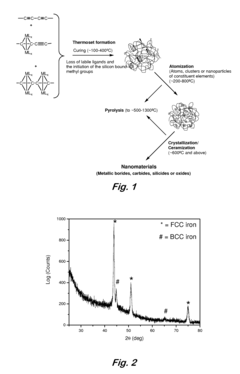
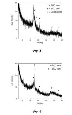
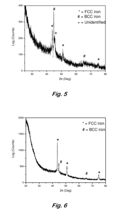
Pyrolytic formation of metallic nanoparticles
PatentActiveUS20080227624A1
Innovation
- A method involving the pyrolysis of diacetylene-containing siloxane polymers at ambient pressure to produce magnetic semiconductors like Fe0.9Co0.1Si and Fe0.1Mn0.9Si, allowing for the formation of metallic nanoparticles and tunable properties by controlling thermal energy and processing conditions.
Materials Characterization Techniques
Advanced characterization techniques are essential for understanding and controlling the surface properties and defects in spintronic materials. Scanning probe microscopy (SPM) techniques, including atomic force microscopy (AFM) and magnetic force microscopy (MFM), provide nanoscale resolution imaging of surface topography and magnetic domain structures. These techniques are particularly valuable for evaluating surface roughness and magnetic homogeneity after modification processes.
X-ray photoelectron spectroscopy (XPS) and Auger electron spectroscopy (AES) offer detailed chemical composition analysis of spintronic material surfaces. XPS can detect changes in chemical states resulting from surface modification treatments, while AES provides excellent spatial resolution for analyzing localized defects and compositional variations across modified surfaces.
Transmission electron microscopy (TEM) and scanning electron microscopy (SEM) are crucial for visualizing structural defects and interface quality. High-resolution TEM enables atomic-scale imaging of lattice defects, grain boundaries, and interface structures that significantly impact spin transport properties. SEM with energy-dispersive X-ray spectroscopy (EDX) capabilities allows for correlating surface morphology with elemental distribution.
For magnetic property characterization, superconducting quantum interference device (SQUID) magnetometry and vibrating sample magnetometry (VSM) provide quantitative measurements of magnetic moments and hysteresis behavior. These techniques help evaluate how surface modifications and defect engineering affect the magnetic performance of spintronic materials.
Synchrotron-based techniques, including X-ray magnetic circular dichroism (XMCD) and resonant inelastic X-ray scattering (RIXS), offer element-specific magnetic information with high sensitivity. These advanced methods can probe spin polarization at interfaces and detect subtle changes in magnetic ordering resulting from defect control strategies.
Time-resolved spectroscopy techniques, such as pump-probe measurements and time-resolved magneto-optical Kerr effect (TR-MOKE), enable the study of spin dynamics and relaxation processes. These measurements are particularly important for understanding how surface modifications influence spin lifetime and transport efficiency in device applications.
In-situ characterization methods that allow real-time monitoring during surface modification processes represent the cutting edge of spintronic materials analysis. These techniques provide valuable insights into modification mechanisms and enable precise control over defect formation and elimination during processing.
Environmental Impact of Spintronic Manufacturing
The manufacturing processes involved in spintronic materials production present significant environmental considerations that warrant careful examination. Traditional semiconductor manufacturing has long been associated with substantial environmental impacts, including high energy consumption, water usage, and hazardous chemical utilization. Spintronic manufacturing inherits many of these challenges while introducing unique environmental concerns related to specialized materials and processes.
Energy consumption represents a primary environmental concern in spintronic manufacturing. The production of high-purity magnetic materials and thin-film deposition processes typically require energy-intensive clean room environments operating continuously. Vacuum systems, plasma generators, and precise temperature control mechanisms collectively contribute to a substantial carbon footprint. Recent industry assessments indicate that advanced spintronic device fabrication can consume 20-30% more energy than conventional semiconductor manufacturing due to additional processing steps.
Water usage presents another critical environmental challenge. Surface modification techniques such as chemical mechanical polishing (CMP) and wet etching processes consume significant quantities of ultra-pure water. A single spintronic manufacturing facility may utilize millions of gallons daily, with water treatment requirements exceeding those of conventional electronics manufacturing due to the presence of magnetic material particulates and specialized chemical compounds.
Chemical waste management poses particular challenges in spintronic manufacturing. The surface modification and defect control processes often employ rare earth elements, heavy metals, and specialized organic solvents. These materials present unique disposal challenges and potential environmental hazards if improperly managed. Industry data suggests that spintronic manufacturing generates approximately 15-25% more hazardous waste per unit area than conventional semiconductor production.
Emerging research indicates potential pathways toward more sustainable spintronic manufacturing. Advanced plasma-based dry etching techniques can reduce chemical waste generation by 40-60% compared to wet chemical processes. Additionally, closed-loop water recycling systems specifically designed for magnetic material particulate removal have demonstrated water consumption reductions of up to 70% in pilot implementations.
Material efficiency improvements represent another promising environmental mitigation strategy. Precise defect control techniques such as atomic layer deposition and molecular beam epitaxy minimize material waste while enhancing device performance. These approaches align environmental sustainability with economic objectives by reducing both resource consumption and manufacturing costs.
Unlock deeper insights with PatSnap Eureka Quick Research — get a full tech report to explore trends and direct your research. Try now!
Generate Your Research Report Instantly with AI Agent
Supercharge your innovation with PatSnap Eureka AI Agent Platform!