

Thermocompression in Consumer Electronics: Application Case Studies
APR 23, 20269 MIN READ
Generate Your Research Report Instantly with AI Agent
PatSnap Eureka helps you evaluate technical feasibility & market potential.
Thermocompression Technology Background and Objectives
Thermocompression technology represents a critical bonding methodology that has evolved significantly since its inception in the semiconductor industry during the 1960s. Originally developed for wire bonding applications in integrated circuits, this technique combines controlled heat and mechanical pressure to create reliable metallurgical bonds between materials. The fundamental principle involves applying simultaneous thermal energy and compressive force to achieve atomic-level diffusion between bonding surfaces, typically involving gold, copper, or aluminum materials.
The historical development of thermocompression bonding can be traced through several evolutionary phases. Initial applications focused primarily on semiconductor packaging, where the need for reliable electrical connections drove technological advancement. As consumer electronics began their rapid expansion in the 1980s and 1990s, thermocompression techniques adapted to meet increasingly demanding requirements for miniaturization, reliability, and cost-effectiveness.
Contemporary consumer electronics present unique challenges that have shaped modern thermocompression objectives. The relentless pursuit of device miniaturization has pushed bonding technologies toward finer pitch capabilities, with current applications requiring bond pad sizes below 50 micrometers. Simultaneously, the proliferation of portable devices has intensified demands for mechanical reliability under various environmental stresses, including thermal cycling, vibration, and humidity exposure.
Current technological objectives center on achieving enhanced bonding precision while maintaining high throughput manufacturing capabilities. Advanced thermocompression systems now target sub-micron placement accuracy combined with process cycle times under 100 milliseconds per bond. These specifications directly support the consumer electronics industry's requirements for high-density interconnects in smartphones, tablets, wearables, and Internet of Things devices.
The integration of smart manufacturing principles has introduced additional objectives related to process monitoring and quality assurance. Modern thermocompression equipment incorporates real-time force and temperature feedback systems, enabling adaptive process control that compensates for material variations and environmental fluctuations. This capability proves essential for maintaining consistent bond quality across high-volume production runs typical in consumer electronics manufacturing.
Environmental sustainability considerations have emerged as increasingly important objectives within thermocompression technology development. Industry initiatives focus on reducing energy consumption through optimized heating profiles and improved thermal management systems. Additionally, the transition toward lead-free materials and environmentally friendly flux formulations has necessitated process parameter optimization to maintain bonding reliability while meeting regulatory compliance requirements.
Future technological objectives emphasize the development of hybrid bonding approaches that combine thermocompression with complementary techniques such as ultrasonic energy or laser heating. These advanced methodologies aim to expand material compatibility while reducing thermal budgets, particularly important for temperature-sensitive components prevalent in modern consumer electronics applications.
Market Demand for Advanced Electronics Assembly
The consumer electronics industry is experiencing unprecedented growth driven by the proliferation of smart devices, wearable technology, and Internet of Things applications. This expansion has created substantial demand for advanced assembly technologies that can accommodate increasingly complex miniaturization requirements while maintaining high reliability standards.
Modern consumer devices require sophisticated packaging solutions to integrate multiple functionalities within compact form factors. Smartphones, tablets, smartwatches, and wireless earbuds exemplify this trend, demanding assembly processes that can handle ultra-thin components, flexible substrates, and heterogeneous material combinations. The market has responded with growing interest in precision bonding technologies that offer superior control over thermal and mechanical parameters.
The automotive electronics sector represents another significant growth driver, particularly with the rise of electric vehicles and autonomous driving systems. Advanced driver assistance systems, infotainment units, and battery management systems require robust assembly methods capable of withstanding harsh operating environments while ensuring long-term reliability. This has intensified demand for assembly technologies that provide excellent thermal conductivity and mechanical stability.
Wearable technology markets continue expanding rapidly, creating unique assembly challenges due to size constraints and flexibility requirements. Fitness trackers, smart glasses, and medical monitoring devices necessitate assembly processes that can work with unconventional substrates and maintain performance under mechanical stress. The industry seeks solutions that enable reliable connections in flexible and stretchable electronics applications.
The 5G infrastructure rollout has generated substantial demand for high-frequency electronic components requiring precise assembly techniques. Base stations, small cells, and network equipment demand assembly methods that minimize signal loss and electromagnetic interference while handling increased power densities. This market segment particularly values assembly technologies that ensure consistent electrical performance across temperature variations.
Consumer expectations for device durability and performance have elevated quality standards throughout the electronics supply chain. Manufacturers face pressure to reduce assembly defects, improve thermal management, and extend product lifespans while controlling costs. This environment favors advanced assembly technologies that offer process repeatability, real-time monitoring capabilities, and reduced material waste compared to traditional methods.
Current State of Thermocompression in Consumer Electronics
Thermocompression technology has established itself as a critical manufacturing process in the consumer electronics industry, particularly in semiconductor packaging and flexible electronics assembly. The current state reveals widespread adoption across multiple product categories, with smartphones, tablets, wearables, and IoT devices representing the primary application domains. Major manufacturers have integrated thermocompression bonding into their production lines to achieve the miniaturization and performance requirements demanded by modern consumer devices.
The technology landscape is dominated by advanced equipment manufacturers such as Kulicke & Soffa, ASM Pacific Technology, and Besi, who have developed sophisticated thermocompression bonding systems capable of handling increasingly complex packaging requirements. These systems now feature precise temperature control within ±2°C, force application accuracy of ±0.5%, and positioning precision at the micrometer level, enabling reliable bonding of components with pitch sizes below 40 micrometers.
Current implementation challenges center around process optimization for diverse material combinations, particularly when bonding dissimilar metals or integrating organic substrates with inorganic components. Temperature management remains critical, as consumer electronics require processing temperatures typically ranging from 150°C to 300°C to avoid damage to heat-sensitive components while ensuring adequate bond strength and electrical conductivity.
The industry has witnessed significant advancement in real-time process monitoring and control systems. Modern thermocompression equipment incorporates advanced sensors for temperature mapping, force feedback mechanisms, and optical inspection systems that enable immediate quality assessment during the bonding process. These developments have improved yield rates to above 99.5% in high-volume manufacturing environments.
Emerging applications include flexible display integration, where thermocompression enables the attachment of driver ICs to flexible substrates without compromising mechanical flexibility. Additionally, the technology has found new relevance in 5G device manufacturing, where enhanced thermal and electrical performance requirements necessitate superior interconnection quality that thermocompression bonding can provide compared to traditional soldering methods.
Current limitations include equipment cost considerations for smaller manufacturers and the need for specialized expertise in process parameter optimization. The technology also faces challenges in handling increasingly diverse material combinations as consumer electronics incorporate new materials for enhanced functionality and sustainability requirements.
Existing Thermocompression Solutions and Methods
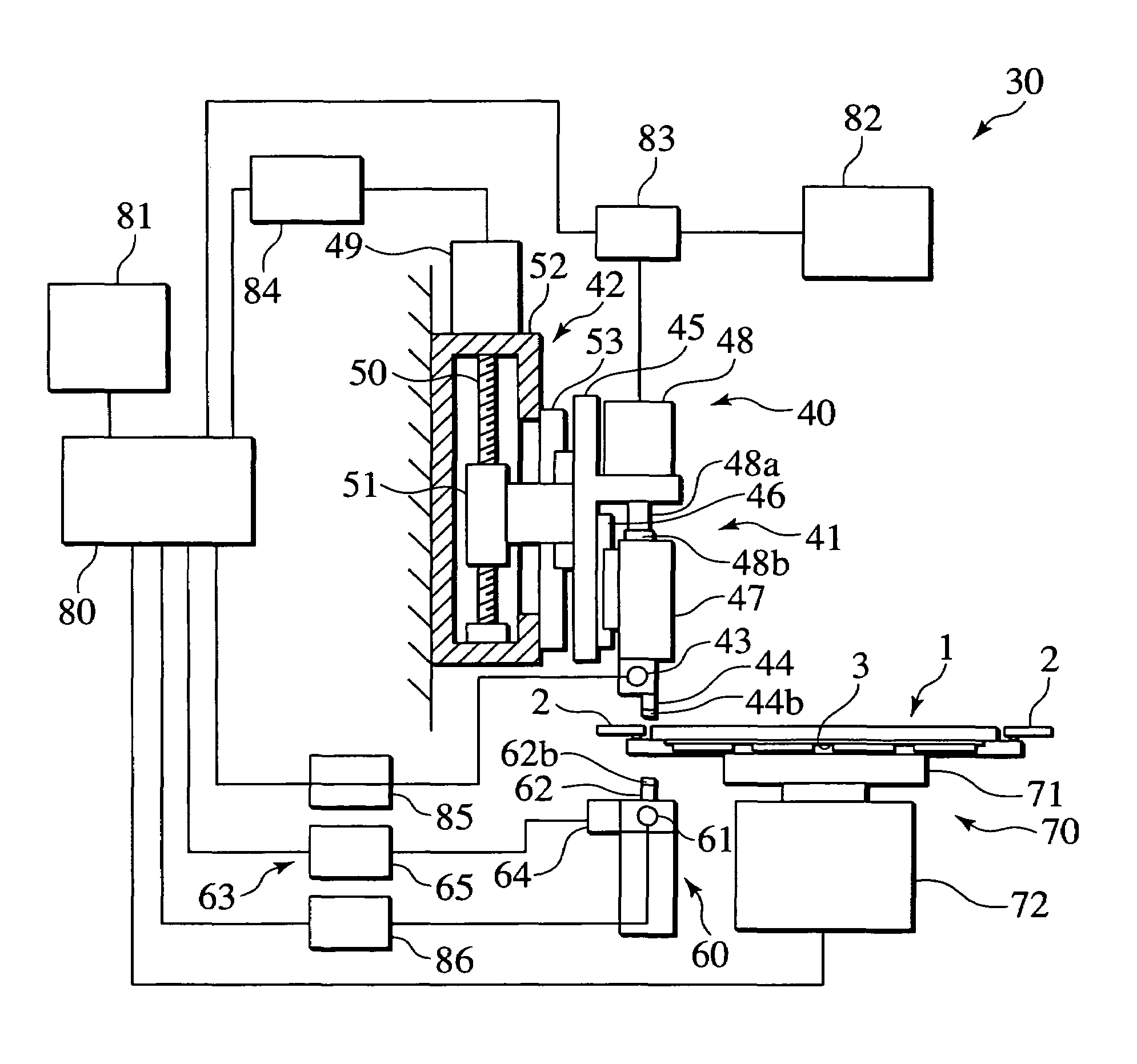
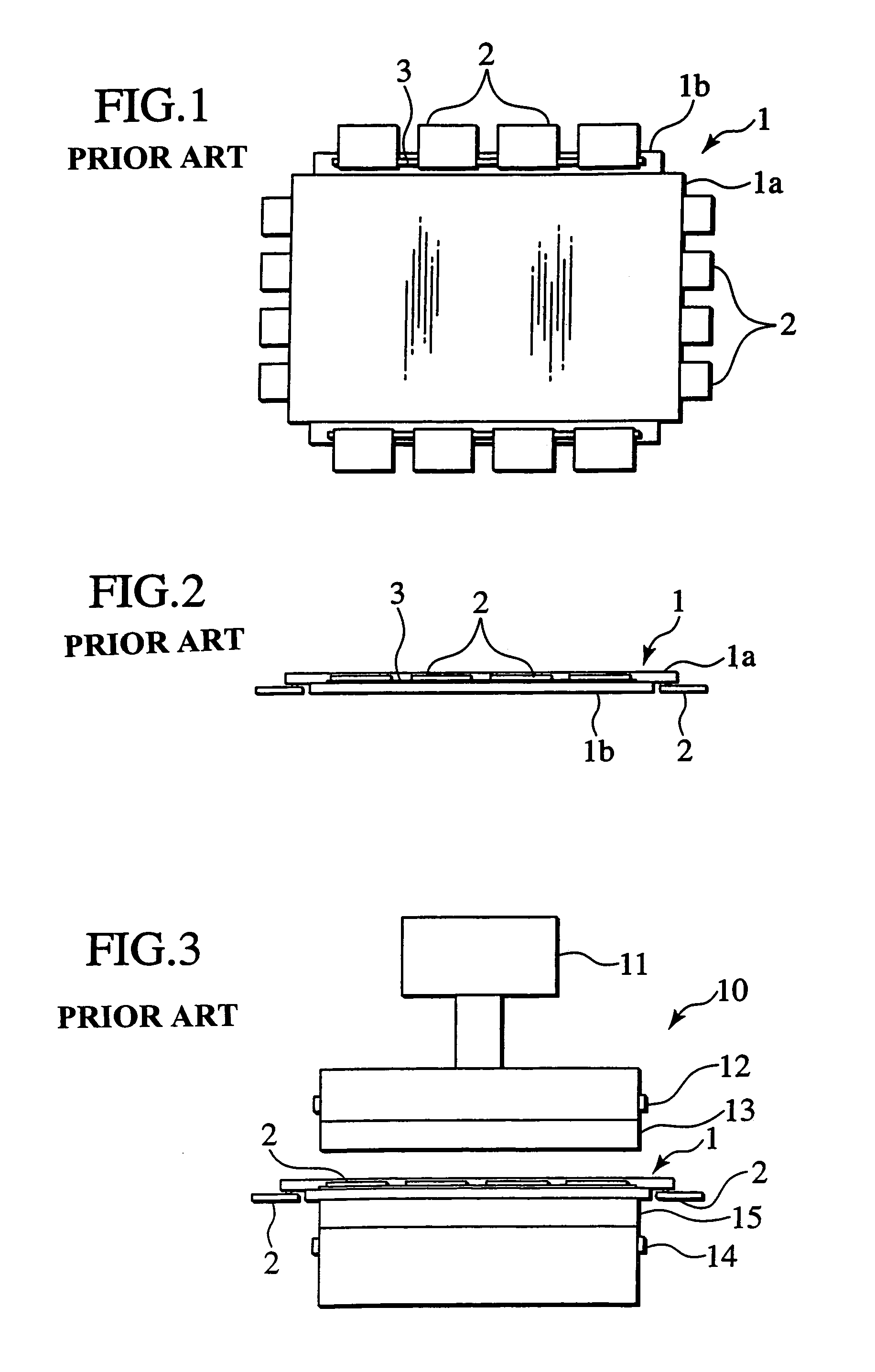
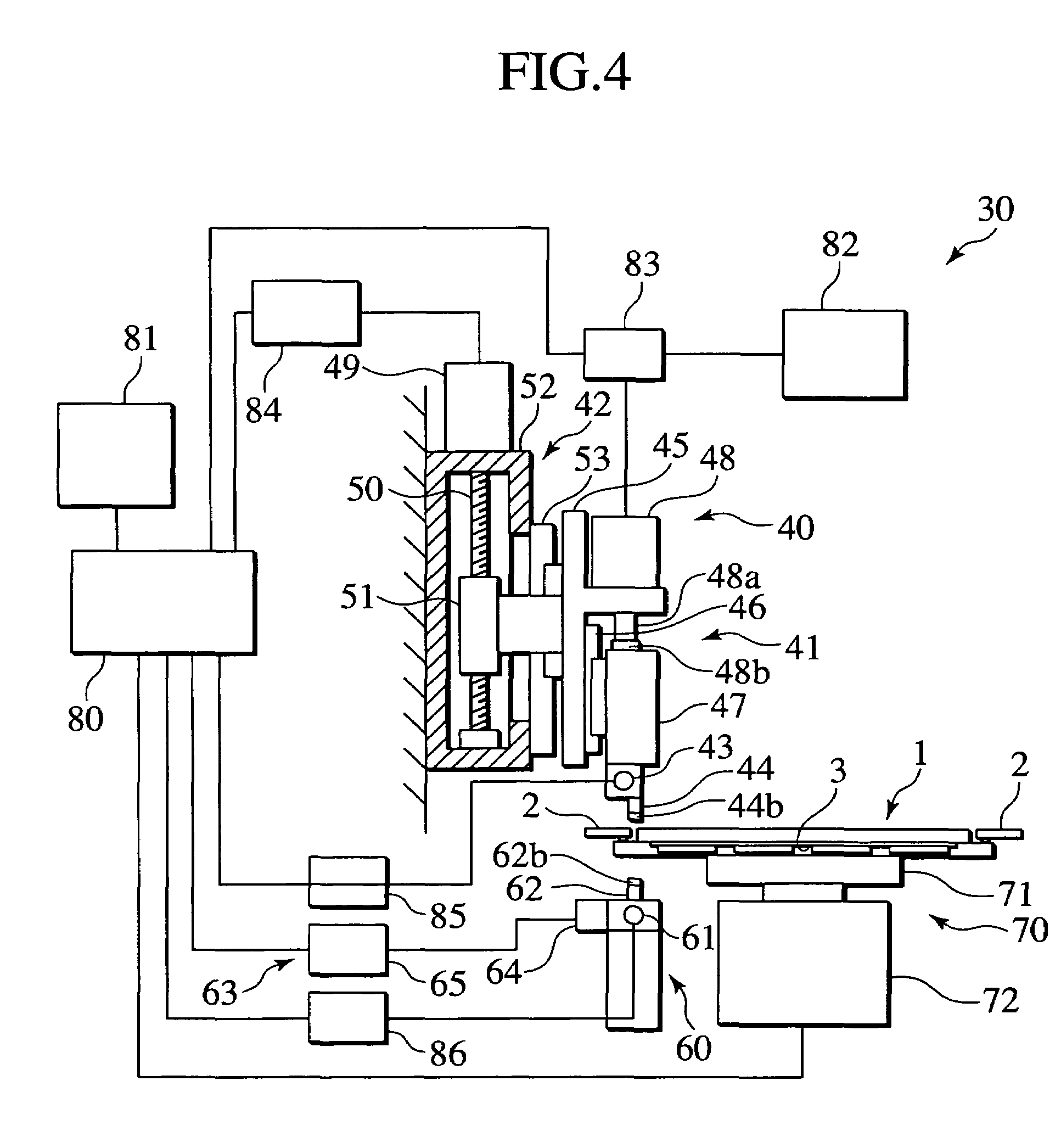
01 Thermocompression bonding apparatus and equipment
Thermocompression bonding apparatus includes specialized equipment designed for applying heat and pressure simultaneously to join materials. These systems typically feature heating elements, pressure application mechanisms, and control systems to regulate temperature and force during the bonding process. The equipment may include automated stages, alignment systems, and monitoring capabilities to ensure precise bonding operations.- Thermocompression bonding apparatus and equipment: Thermocompression bonding apparatus includes specialized equipment designed for applying heat and pressure simultaneously to join materials. These systems typically feature heating elements, pressure application mechanisms, and control systems to regulate temperature and force during the bonding process. The equipment may include automated stages, alignment systems, and monitoring capabilities to ensure precise bonding operations.
- Thermocompression bonding methods and processes: Various methods and processes for thermocompression bonding involve specific sequences of heating, pressing, and cooling steps. These processes may include pre-heating stages, controlled pressure application profiles, and optimized temperature cycles to achieve strong bonds. The methods can be adapted for different materials and applications, with considerations for bonding time, temperature ranges, and pressure levels to ensure reliable connections.
- Semiconductor packaging using thermocompression: Thermocompression bonding is widely used in semiconductor packaging for connecting chips to substrates or lead frames. This application involves bonding metal bumps or wires to contact pads using controlled heat and pressure. The process enables fine-pitch connections, high-density packaging, and reliable electrical interconnections in integrated circuits and electronic devices.
- Thermocompression bonding tools and components: Specialized tools and components for thermocompression bonding include bonding heads, heating tips, pressure sensors, and positioning mechanisms. These components are designed to deliver precise heat and force to the bonding area while maintaining alignment and control. The tools may feature replaceable tips, temperature monitoring systems, and force feedback mechanisms to optimize bonding quality.
- Advanced thermocompression applications and materials: Advanced applications of thermocompression bonding extend to various materials including metals, polymers, and composite structures. These applications may involve multi-layer bonding, heterogeneous material joining, and specialized surface treatments. The technology enables bonding of dissimilar materials, creation of hermetic seals, and formation of complex assemblies in electronics, automotive, and aerospace industries.
02 Thermocompression bonding methods and processes
Various methods and processes for thermocompression bonding involve specific sequences of heating, pressing, and cooling steps. These processes may include pre-heating stages, controlled pressure application profiles, and optimized temperature cycles to achieve strong bonds. The methods can be adapted for different materials and applications, including semiconductor packaging, flexible electronics, and multi-layer structures.Expand Specific Solutions03 Thermocompression bonding tools and heads
Specialized bonding tools and heads are designed for thermocompression applications, featuring specific geometries, heating elements, and force distribution characteristics. These tools may include capillary designs, wedge configurations, or flat bonding surfaces depending on the application. The tools are engineered to provide uniform heat and pressure distribution while minimizing damage to delicate components.Expand Specific Solutions04 Thermocompression bonding for semiconductor and electronic packaging
Thermocompression bonding techniques are widely applied in semiconductor and electronic packaging for creating electrical and mechanical connections. Applications include wire bonding, flip-chip bonding, and die attachment processes. The technology enables fine-pitch interconnections, three-dimensional packaging structures, and reliable connections in advanced electronic devices while maintaining component integrity.Expand Specific Solutions05 Thermocompression bonding parameters and control systems
Control systems and parameter optimization for thermocompression bonding focus on regulating temperature, pressure, bonding time, and environmental conditions. Advanced control methods may include feedback mechanisms, real-time monitoring, and adaptive algorithms to ensure consistent bonding quality. Parameters are carefully selected based on material properties, joint requirements, and process constraints to achieve optimal bonding strength and reliability.Expand Specific Solutions
Key Players in Thermocompression Equipment Industry
The thermocompression technology in consumer electronics is experiencing rapid growth driven by miniaturization demands and advanced packaging requirements. The industry is in a mature development stage with significant market expansion, particularly in semiconductor packaging and flexible electronics applications. Technology maturity varies significantly across market players, with established semiconductor giants like Intel Corp., Samsung Electronics, and Apple leading in advanced implementation capabilities. Traditional electronics manufacturers including Sony Group Corp., Canon Inc., and Huawei Technologies demonstrate strong integration expertise, while specialized equipment providers such as Shibaura Mechatronics Corp. and Han's Laser Technology focus on manufacturing solutions. Academic institutions like Tsinghua University and Northeastern University contribute fundamental research, indicating robust innovation pipelines. The competitive landscape shows consolidation around key technological capabilities, with companies like tesa SE providing critical materials expertise, positioning the market for continued technological advancement and commercial expansion.
Intel Corp.
Technical Solution: Intel utilizes thermocompression bonding technology in their processor packaging for consumer laptops and desktop computers. Their process involves controlled heating to 160-220°C combined with mechanical pressure for creating reliable solder joints and interconnections in CPU packages. Intel has developed specialized thermocompression equipment that enables fine-pitch bonding with pad sizes down to 40μm, essential for high-performance consumer processors with increasing transistor density and thermal management requirements.
Strengths: Advanced packaging technology leadership and robust thermal management solutions. Weaknesses: Higher complexity and cost compared to traditional bonding methods, primarily suited for high-end applications.
Samsung Electronics Co., Ltd.
Technical Solution: Samsung implements thermocompression bonding extensively in their semiconductor packaging for consumer electronics, including smartphones, tablets, and wearables. Their advanced thermocompression process operates at temperatures ranging from 120-180°C with precise force control for wire bonding and die attachment applications. Samsung has integrated automated thermocompression systems that achieve bonding cycle times under 50ms while maintaining bond strength exceeding 10gf for reliable consumer device performance.
Strengths: Comprehensive semiconductor manufacturing capabilities and cost-effective high-volume production. Weaknesses: Technology primarily focused on internal use with limited external licensing opportunities.
Core Patents in Consumer Electronics Thermocompression
Electronic part compression bonding apparatus and method
PatentInactiveUS7075036B2
Innovation
- The solution involves an electronic part compression bonding apparatus that variably controls pressure and heating conditions based on the elongation properties of the electronic parts, using a thermocompression bonding control unit to adjust pressure and temperature settings during the bonding process, allowing for precise control of elongation through multiple stages and the use of a cooling unit to manage temperature.

Thermocompression device and method of manufacturing display device using same
PatentWO2022039290A1
Innovation
- A thermal compression device is used to collectively heat-press a semiconductor light-emitting device array onto a wiring board, employing a lower head to support the board, an upper head to apply pressure, and suction grooves to manage pressure and alignment, ensuring proper connection and minimizing curling issues.


Manufacturing Standards for Thermocompression Processes
The establishment of comprehensive manufacturing standards for thermocompression processes in consumer electronics has become increasingly critical as device miniaturization and performance demands continue to escalate. Current industry standards primarily focus on temperature control protocols, pressure application parameters, and bonding quality metrics that ensure consistent and reliable interconnections in electronic assemblies.
International standards organizations, including IPC and JEDEC, have developed specific guidelines for thermocompression bonding operations. These standards define acceptable temperature ranges typically between 150°C to 300°C, depending on the substrate materials and bonding requirements. Pressure specifications generally range from 20 to 200 grams-force per bond, with precise control mechanisms required to maintain uniformity across multiple bonding sites.
Quality assurance protocols within these standards emphasize real-time monitoring of critical process variables. Temperature uniformity across the bonding interface must be maintained within ±5°C tolerance, while pressure application timing is standardized to prevent over-compression or insufficient bonding force. These parameters are particularly crucial for fine-pitch applications where bond pad dimensions continue to shrink.
Material compatibility standards address the interaction between different substrate materials, wire compositions, and protective coatings used in thermocompression processes. Standards specify acceptable material combinations and highlight potential incompatibilities that could lead to intermetallic compound formation or bond degradation over time.
Process validation requirements mandate comprehensive testing protocols including pull tests, shear strength measurements, and thermal cycling evaluations. These standards ensure that thermocompression bonds maintain their integrity under operational stress conditions typical in consumer electronics applications.
Environmental control standards address cleanroom requirements, humidity levels, and contamination prevention measures essential for achieving consistent bonding results. These specifications are particularly stringent for high-reliability applications where bond failure could compromise device functionality.
Emerging standards development focuses on advanced materials integration, including flexible substrates and novel conductor materials, reflecting the evolving landscape of consumer electronics manufacturing requirements.
Cost-Benefit Analysis of Thermocompression Implementation
The economic evaluation of thermocompression implementation in consumer electronics reveals a complex landscape of initial investments versus long-term operational benefits. Manufacturing facilities typically face substantial upfront capital expenditures ranging from $2-8 million for comprehensive thermocompression equipment integration, depending on production scale and automation levels. These costs encompass specialized bonding machines, precision temperature control systems, and necessary cleanroom infrastructure modifications.
Equipment acquisition represents approximately 60-70% of total implementation costs, while facility preparation and staff training account for the remaining investment. Advanced thermocompression systems require controlled environments with temperature stability within ±1°C and humidity control below 45% RH, necessitating HVAC system upgrades that can add $500,000-1.5 million to project budgets.
Operational cost analysis demonstrates significant long-term advantages through reduced material waste and enhanced yield rates. Thermocompression processes typically achieve 95-98% first-pass yield compared to 85-90% for conventional assembly methods, translating to material savings of 8-15% annually. Energy consumption patterns show mixed results, with higher initial heating requirements offset by reduced rework cycles and shorter overall processing times.
Labor cost implications vary significantly across implementation scales. While thermocompression requires specialized operator training with associated costs of $15,000-25,000 per technician, the technology enables higher throughput rates that can reduce per-unit labor costs by 12-18%. Automated systems further amplify these benefits, though they require additional maintenance expertise and spare parts inventory.
Return on investment calculations indicate payback periods of 18-36 months for high-volume consumer electronics manufacturing, with premium product segments achieving faster returns due to higher profit margins. Quality-related cost reductions, including decreased warranty claims and field failures, contribute an additional 3-7% to overall cost savings. Market positioning advantages from enhanced product reliability and miniaturization capabilities provide intangible benefits that strengthen competitive positioning and support premium pricing strategies in consumer electronics markets.
Unlock deeper insights with PatSnap Eureka Quick Research — get a full tech report to explore trends and direct your research. Try now!
Generate Your Research Report Instantly with AI Agent
Supercharge your innovation with PatSnap Eureka AI Agent Platform!