Ultrafast Lasers in Advanced Superconductive Material Processing.
SEP 4, 20259 MIN READ
Generate Your Research Report Instantly with AI Agent
PatSnap Eureka helps you evaluate technical feasibility & market potential.
Ultrafast Laser Technology Evolution and Objectives
Ultrafast laser technology has evolved significantly since its inception in the 1960s with the development of Q-switching and mode-locking techniques. The journey from nanosecond to femtosecond pulse durations represents a revolutionary advancement in laser physics, enabling unprecedented precision in material processing applications. Early ultrafast lasers were primarily confined to laboratory settings due to their complexity and maintenance requirements, limiting their industrial adoption despite their theoretical advantages for superconductor processing.
The 1990s marked a turning point with the commercialization of Ti:Sapphire laser systems, offering more reliable femtosecond pulses. However, these systems remained bulky and required specialized knowledge to operate. The early 2000s witnessed the emergence of fiber-based ultrafast lasers, providing more compact and stable platforms for industrial applications, though still with limitations in power scaling for demanding material processing tasks.
Recent developments have focused on diode-pumped solid-state (DPSS) ultrafast lasers and high-power fiber laser architectures, achieving remarkable combinations of pulse energy, repetition rate, and beam quality. These advancements have made ultrafast lasers increasingly viable for precision manufacturing, including the processing of superconductive materials where thermal effects must be minimized to preserve critical properties.
The current technological trajectory aims to overcome several key challenges in ultrafast laser technology for superconductor processing. Primary objectives include achieving higher average powers while maintaining ultrashort pulse durations, improving beam quality for enhanced focusing capabilities, and developing more sophisticated pulse shaping techniques to optimize interaction with superconductive materials. Additionally, there is a push toward more user-friendly systems that require less specialized knowledge to operate, facilitating broader industrial adoption.
Another critical objective is the development of real-time monitoring and feedback systems that can adjust laser parameters on-the-fly based on material response, ensuring consistent processing quality across varying superconductor compositions and geometries. This adaptive processing capability is particularly important for high-temperature superconductors with complex crystalline structures.
Looking forward, the field is moving toward multi-beam and spatial light modulator approaches that allow parallel processing to increase throughput while maintaining the precision advantages of ultrafast lasers. Integration with advanced automation and machine learning algorithms represents the next frontier, potentially enabling autonomous optimization of laser parameters for specific superconductor processing tasks and accelerating the discovery of novel processing techniques.
Market Analysis for Superconductor Manufacturing
The global superconductor manufacturing market is experiencing significant growth, driven by advancements in ultrafast laser processing technologies. Current market valuations place the superconductor industry at approximately 7.5 billion USD, with projections indicating a compound annual growth rate of 17% through 2030. This remarkable expansion is fueled by increasing demand across multiple sectors including quantum computing, medical imaging, transportation, and energy transmission systems.
The healthcare segment represents the largest market share, with MRI machines utilizing superconducting magnets accounting for nearly 30% of the total market. This dominance is expected to continue as healthcare infrastructure expands globally, particularly in emerging economies. The energy sector follows closely behind, with superconducting cables and transformers gaining traction as utilities seek more efficient power transmission solutions that can reduce energy losses by up to 90% compared to conventional systems.
Regionally, North America currently leads the market with approximately 35% share, followed by Asia-Pacific at 30% and Europe at 25%. However, the most rapid growth is occurring in the Asia-Pacific region, particularly in China, Japan, and South Korea, where government initiatives are heavily supporting superconductor research and manufacturing capabilities. China's investment in superconductor technology has increased by over 200% in the past five years, positioning it to potentially overtake traditional market leaders.
The integration of ultrafast laser processing in superconductor manufacturing has created a specialized sub-market estimated at 850 million USD, growing at 22% annually. This premium segment is characterized by higher margins and technological barriers to entry, attracting specialized equipment manufacturers and material science companies.
Customer segmentation reveals three primary buyer categories: research institutions (15% of market), industrial manufacturers (55%), and government/defense contractors (30%). Each segment demonstrates distinct purchasing behaviors and requirements, with industrial manufacturers prioritizing scalability and cost-effectiveness, while research institutions focus on precision and customization capabilities.
Market challenges include high manufacturing costs, with specialized superconducting materials costing up to 100 times more than conventional conductors. Supply chain vulnerabilities also persist, particularly for rare earth elements essential to certain superconductor types. Additionally, the technical expertise required for implementation creates adoption barriers in emerging markets.
Despite these challenges, the market outlook remains highly positive, with ultrafast laser processing technologies expected to reduce manufacturing costs by up to 40% over the next decade, potentially unlocking new application areas and accelerating market penetration across previously cost-prohibitive sectors.
Current Capabilities and Barriers in Ultrafast Laser Processing
Ultrafast laser processing of superconductive materials represents a frontier technology with significant capabilities and limitations in current applications. The femtosecond and picosecond pulse durations characteristic of ultrafast lasers enable precise material removal with minimal heat-affected zones, a critical advantage when working with temperature-sensitive superconductors where thermal damage can compromise superconducting properties.
Current capabilities include the ability to achieve sub-micron feature sizes in superconducting thin films, particularly important for quantum computing circuit fabrication where precise Josephson junction dimensions are essential. The non-thermal ablation mechanism of ultrafast lasers allows for clean material removal without the formation of recast layers or micro-cracks that plague conventional laser processing methods.
Advanced beam shaping techniques have further enhanced processing capabilities, with spatial light modulators enabling complex pattern generation in single exposures. This has proven particularly valuable for creating intricate superconducting quantum interference device (SQUID) geometries without multiple processing steps. Additionally, recent developments in burst-mode processing have demonstrated improved ablation efficiency while maintaining the non-thermal advantages of ultrafast processing.
Despite these advances, significant barriers remain in the widespread implementation of ultrafast laser processing for superconducting materials. Foremost among these is the challenge of processing speed versus precision trade-offs. While ultrafast lasers excel at high-precision micromachining, their throughput remains limited compared to conventional techniques, creating bottlenecks in industrial-scale production of superconducting devices.
Material-specific challenges also persist, particularly with high-temperature superconductors (HTS) like YBCO, which exhibit complex stoichiometry that can be disrupted during laser processing. Maintaining the exact oxygen content critical for superconducting properties remains difficult even with ultrafast processing. Additionally, the multi-layered structures common in practical superconducting devices present challenges in achieving uniform processing quality across heterogeneous material interfaces.
Equipment costs represent another significant barrier, with industrial-grade ultrafast laser systems requiring investments of several hundred thousand dollars, limiting accessibility particularly for research institutions and smaller manufacturers. The complexity of these systems also necessitates specialized technical expertise for operation and maintenance, further restricting widespread adoption.
Process monitoring and quality control remain underdeveloped areas, with real-time feedback systems for ultrafast laser processing of superconductors still in early research stages. The lack of standardized processing parameters across different superconducting material systems further complicates industrial implementation, requiring extensive empirical optimization for each new material combination.
Established Methodologies for Superconductive Material Processing
01 Ultrafast laser pulse generation and control
Ultrafast lasers generate extremely short pulses, typically in the femtosecond to picosecond range. These systems employ various techniques for pulse generation, including mode-locking, Q-switching, and cavity dumping. Advanced control mechanisms allow for precise manipulation of pulse characteristics such as duration, repetition rate, and energy. These technologies enable applications requiring high temporal precision and peak power while maintaining beam quality and stability.- Ultrafast laser pulse generation and control: Ultrafast lasers generate extremely short pulses, typically in the femtosecond to picosecond range. These systems employ various techniques for pulse generation, including mode-locking, Q-switching, and cavity dumping. Advanced control mechanisms allow for precise manipulation of pulse characteristics such as duration, repetition rate, and energy. These technologies enable applications requiring high temporal resolution and peak power while maintaining beam quality and stability.
- Medical and surgical applications of ultrafast lasers: Ultrafast lasers offer significant advantages in medical procedures due to their ability to deliver precise energy with minimal thermal damage to surrounding tissues. These systems are particularly valuable in ophthalmology for corneal and retinal surgeries, dermatology for skin treatments, and microsurgery applications. The non-thermal ablation mechanism allows for clean tissue removal without collateral damage, enabling more precise interventions and faster healing times compared to conventional laser systems.
- Material processing and manufacturing with ultrafast lasers: Ultrafast lasers enable high-precision material processing across various industries. Their extremely short pulse duration allows for cold ablation processes where material is removed with minimal heat-affected zones, making them ideal for micromachining, drilling, cutting, and surface modification of sensitive materials. These capabilities are particularly valuable for processing semiconductors, ceramics, polymers, and metals in applications requiring micrometer or nanometer precision.
- Optical communication and data processing systems: Ultrafast lasers play a crucial role in high-speed optical communication networks and data processing systems. Their ability to generate precisely timed pulses enables high data transmission rates and signal processing capabilities. These systems are used in telecommunications infrastructure, data centers, and quantum information processing. The technology allows for multiplexing techniques that significantly increase bandwidth and enable advanced optical signal processing for next-generation communication networks.
- Scientific research and metrology applications: Ultrafast lasers are essential tools in scientific research and precision measurement applications. Their extremely short pulses enable time-resolved spectroscopy for studying ultrafast phenomena in physics, chemistry, and biology. These systems are used in pump-probe experiments, attosecond science, and frequency comb generation for precision metrology. The technology allows researchers to observe and measure processes occurring at previously inaccessible timescales, advancing fundamental understanding across multiple scientific disciplines.
02 Medical and surgical applications of ultrafast lasers
Ultrafast lasers offer significant advantages in medical procedures due to their minimal thermal effects on surrounding tissues. These lasers enable precise ablation and cutting with reduced collateral damage, making them ideal for delicate procedures in ophthalmology, dermatology, and neurosurgery. The non-linear absorption properties of ultrafast pulses allow for subsurface tissue modification without damaging intervening layers, enabling novel therapeutic approaches and improved surgical outcomes.Expand Specific Solutions03 Material processing and manufacturing with ultrafast lasers
Ultrafast lasers enable high-precision material processing with minimal heat-affected zones. The extremely short pulse duration allows for cold ablation processes where material is removed before heat can diffuse to surrounding areas. This capability is particularly valuable for micromachining, drilling, cutting, and surface texturing of various materials including metals, semiconductors, ceramics, and polymers. These lasers can achieve feature sizes below the diffraction limit through non-linear absorption effects.Expand Specific Solutions04 Ultrafast laser amplification and power scaling
Various amplification techniques are employed to increase the power and energy of ultrafast laser pulses while preserving their temporal characteristics. Chirped pulse amplification (CPA) stretches pulses temporally before amplification to avoid damage to optical components, then recompresses them afterward. Optical parametric amplification offers broad gain bandwidth for supporting ultrashort pulses. These approaches enable the generation of high-energy ultrafast pulses for applications requiring extreme intensities.Expand Specific Solutions05 Imaging and sensing applications of ultrafast lasers
Ultrafast lasers enable advanced imaging and sensing techniques with unprecedented temporal and spatial resolution. These include multiphoton microscopy, pump-probe spectroscopy, and terahertz generation for non-destructive testing. The short pulse duration allows for time-resolved studies of ultrafast phenomena in physics, chemistry, and biology. Additionally, frequency comb technology derived from ultrafast lasers provides precise frequency references for metrology, spectroscopy, and timing applications.Expand Specific Solutions
Industry Leaders in Ultrafast Laser and Superconductor Sectors
The ultrafast laser market for superconductive material processing is currently in a growth phase, with an expanding market size driven by increasing applications in semiconductor manufacturing and quantum computing. The technology maturity varies across players, with established companies like Coherent, Inc. and IMRA America leading commercial innovation through their extensive laser product portfolios and processing solutions. Research institutions such as Harbin Institute of Technology, Wuhan University, and Korea Research Institute of Standards & Science are advancing fundamental science in this domain. Companies like Electro Scientific Industries and Han's Laser are developing specialized industrial applications, while academic-industrial partnerships between institutions like University of Michigan and commercial entities are accelerating technology transfer. The competitive landscape shows a geographic concentration in North America, East Asia, and Europe.
IMRA America, Inc.
Technical Solution: IMRA America has pioneered femtosecond fiber laser technology specifically optimized for superconducting material processing. Their FCPA (Fiber Chirped Pulse Amplification) µJewel system delivers ultrashort pulses (< 500 fs) with high repetition rates (up to 5 MHz) and precise energy control, enabling cold ablation processing of high-temperature superconductors (HTS) like YBCO and MgB2. Their proprietary technology allows for material removal with minimal heat-affected zones (<2 μm), critical for maintaining superconducting properties. IMRA has developed specialized beam shaping techniques that create uniform energy distribution across the processing area, resulting in consistent material modification without compromising superconducting transition temperatures. Their systems incorporate real-time monitoring that adjusts laser parameters based on material feedback, ensuring optimal processing conditions for different superconductor compositions.
Strengths: Industry-leading femtosecond fiber laser technology with exceptional pulse stability (jitter <100 fs); proprietary beam shaping technology for uniform energy distribution; integrated real-time monitoring systems. Weaknesses: Higher initial equipment cost compared to conventional laser systems; requires specialized knowledge for operation; limited throughput for large-scale industrial applications.
Electro Scientific Industries, Inc.
Technical Solution: ESI has developed the GenesisXP ultrafast laser processing system specifically designed for superconducting material applications. Their technology utilizes picosecond lasers (pulse duration 10-15 ps) with high pulse energy stability (<1% RMS) and beam positioning accuracy of ±1 μm, critical for creating precise Josephson junctions and superconducting quantum interference devices (SQUIDs). ESI's proprietary PulseEQ technology enables dynamic control of pulse energy distribution across the beam profile, allowing for tailored energy deposition that preserves the crystalline structure of superconducting materials. Their systems incorporate specialized beam delivery optics that maintain polarization state throughout the optical path, ensuring consistent material interaction regardless of feature orientation. ESI has also developed advanced process monitoring techniques that analyze plasma emissions during ablation to provide real-time feedback on material removal rates and quality, essential for maintaining superconducting properties.
Strengths: Exceptional beam positioning accuracy and pulse energy stability; proprietary PulseEQ technology for controlled energy distribution; advanced process monitoring capabilities; specialized expertise in micromachining applications. Weaknesses: Limited to picosecond regime (vs. femtosecond competitors); higher operational complexity; more sensitive to environmental conditions affecting long-term stability.
Critical Patents and Research in Ultrafast Laser-Material Interaction
Laser system and method for material processing with ultra fast lasers
PatentInactiveUS6979798B2
Innovation
- A method and system utilizing a single ultra-short laser pulse with a pulse width less than the characteristic breakdown point, focused to achieve high energy density without damaging adjacent non-target materials, employing chirped pulse amplification and fiber-based laser systems to generate pulses shorter than 10 ps, and using sacrificial layers for non-linear absorption and shielding.


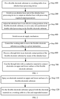
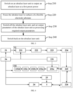
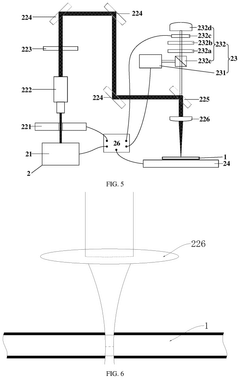
Ultrafast laser processing method for flexible double-sided electrodes
PatentPendingUS20250128350A1
Innovation
- An ultrafast laser processing method for flexible double-sided electrodes, which involves fixing a flexible electrode substrate to an ultrafast laser processing device, adjusting the laser to an effective acting position for synchronized double-sided processing, and optionally processing through holes and coating with conductive material.
Energy Efficiency Considerations in Advanced Manufacturing
Energy efficiency has emerged as a critical consideration in the application of ultrafast lasers for superconductive material processing. The inherently high peak power of ultrafast laser systems, while essential for precision material modification, presents significant energy consumption challenges. Current ultrafast laser systems typically operate at 5-15% wall-plug efficiency, with substantial energy losses occurring during the amplification stages and thermal management systems. This inefficiency becomes particularly pronounced in industrial-scale applications where continuous operation is required.
Recent advancements in laser architecture have begun addressing these concerns through several innovative approaches. Fiber-based ultrafast laser systems demonstrate improved efficiency (up to 30%) compared to traditional solid-state systems, while requiring less intensive cooling infrastructure. Additionally, the implementation of regenerative amplification techniques has shown promise in recycling unused pulse energy, potentially increasing overall system efficiency by 10-15% in laboratory settings.
Energy recovery systems represent another frontier in efficiency improvement. Thermal energy, previously considered waste, is now being captured and repurposed in integrated manufacturing environments. Advanced facilities have implemented heat exchangers that redirect thermal output from laser cooling systems to support other manufacturing processes or facility heating requirements, achieving up to 25% reduction in total energy footprint.
The processing of superconductive materials presents unique efficiency considerations due to their temperature-sensitive properties. Conventional approaches often require energy-intensive cryogenic environments during processing. Ultrafast laser techniques enable "cold processing" paradigms where material modification occurs through non-thermal pathways, significantly reducing the energy required for temperature management. Studies indicate energy savings of 40-60% compared to traditional methods when processing high-temperature superconductors.
Pulse management strategies further enhance energy efficiency through adaptive control systems. Real-time monitoring and adjustment of laser parameters based on material response optimize energy delivery, preventing overprocessing and unnecessary energy expenditure. Advanced systems incorporating machine learning algorithms have demonstrated the ability to reduce energy consumption by up to 35% while maintaining or improving processing quality through predictive parameter optimization.
The industry is moving toward integrated energy management frameworks that consider the entire manufacturing ecosystem rather than isolated laser systems. This holistic approach encompasses energy-efficient facility design, optimized production scheduling, and comprehensive energy recovery systems. Leading manufacturers have reported overall energy efficiency improvements of 20-30% through such integrated approaches, establishing new benchmarks for sustainable advanced manufacturing practices.
Quantum Applications and Integration Possibilities
The integration of ultrafast laser technology with quantum systems represents a frontier with extraordinary potential for advancing superconducting material applications. Quantum computing architectures utilizing superconducting qubits can benefit significantly from precision material processing enabled by ultrafast lasers. These lasers facilitate the creation of highly uniform Josephson junctions—critical components in superconducting quantum circuits—with unprecedented accuracy at the nanoscale level, potentially increasing qubit coherence times and computational fidelity.
Quantum sensing applications represent another promising integration pathway. Ultrafast laser-processed superconducting materials exhibit enhanced quantum sensing capabilities, particularly in detecting weak magnetic fields with SQUID (Superconducting Quantum Interference Device) magnetometers. The precise material structuring achievable with femtosecond lasers allows for optimized flux coupling and reduced noise floors in these quantum-limited sensors, enabling applications from medical imaging to fundamental physics research.
Quantum communication networks could leverage ultrafast laser-processed superconducting nanowire single-photon detectors (SNSPDs) with improved detection efficiency and timing resolution. The ability to precisely engineer the geometry and composition of superconducting nanowires through ultrafast laser processing translates directly to enhanced quantum key distribution systems and secure quantum networks.
The quantum metrology field stands to gain from this technological convergence as well. Superconducting circuits processed with ultrafast lasers can serve as quantum-limited amplifiers and frequency standards with exceptional stability. These components form the backbone of next-generation quantum measurement systems that approach fundamental precision limits.
Hybrid quantum systems combining superconducting circuits with other quantum technologies (such as trapped ions or spin qubits) represent perhaps the most ambitious integration possibility. Ultrafast laser processing enables the creation of precise interfaces between disparate quantum systems, facilitating coherent information transfer across different physical platforms. This hybridization approach may overcome the inherent limitations of individual quantum technologies.
Looking forward, the development of integrated quantum photonic circuits incorporating laser-processed superconducting elements could enable on-chip quantum information processing with both superconducting and photonic qubits. This convergence of technologies points toward a future where quantum advantages can be realized across multiple application domains simultaneously, from computation to sensing to secure communications.
Unlock deeper insights with PatSnap Eureka Quick Research — get a full tech report to explore trends and direct your research. Try now!
Generate Your Research Report Instantly with AI Agent
Supercharge your innovation with PatSnap Eureka AI Agent Platform!