Wafer-Level Optics Vs Micro-Lens Arrays: Implementation Cost Analysis
APR 9, 20269 MIN READ
Generate Your Research Report Instantly with AI Agent
Patsnap Eureka helps you evaluate technical feasibility & market potential.
Wafer-Level Optics vs Micro-Lens Arrays Background and Objectives
The optical industry has witnessed significant evolution in miniaturization technologies, with wafer-level optics and micro-lens arrays emerging as two dominant approaches for compact optical systems. Both technologies address the growing demand for smaller, lighter, and more cost-effective optical components across consumer electronics, automotive sensors, medical devices, and telecommunications equipment. The convergence of these fields represents a critical juncture where manufacturing scalability meets performance requirements.
Wafer-level optics technology leverages semiconductor fabrication processes to create optical elements directly on wafer substrates, enabling mass production of miniaturized optical components. This approach has gained momentum due to its compatibility with existing semiconductor manufacturing infrastructure and potential for high-volume production. The technology encompasses various fabrication techniques including photolithography, etching, and replication processes that can produce complex optical surfaces with high precision.
Micro-lens arrays, conversely, represent a more established technology that focuses on creating arrays of small lenses through techniques such as thermal reflow, photoresist patterning, and molding processes. These arrays have found widespread applications in beam shaping, light homogenization, and optical coupling systems. The technology has matured significantly over the past decade, with improvements in manufacturing precision and cost reduction.
The primary objective of this comparative analysis centers on understanding the implementation cost structures of both technologies across different production volumes and application scenarios. This evaluation aims to identify the break-even points where one technology becomes more economically viable than the other, considering factors such as initial capital investment, material costs, yield rates, and scalability potential.
Furthermore, this analysis seeks to establish a comprehensive framework for decision-making in optical system design, particularly for applications requiring high-volume production. The investigation will examine how manufacturing complexity, quality control requirements, and supply chain considerations impact the total cost of ownership for each technology approach.
The ultimate goal involves providing actionable insights for technology selection based on specific application requirements, production volumes, and cost constraints, thereby enabling more informed strategic decisions in optical system development and manufacturing planning.
Market Demand Analysis for Miniaturized Optical Solutions
The miniaturized optical solutions market is experiencing unprecedented growth driven by the convergence of multiple technological trends and consumer demands. The proliferation of mobile devices, augmented reality systems, and Internet of Things applications has created substantial demand for compact, high-performance optical components that can deliver superior functionality within increasingly constrained form factors.
Consumer electronics represent the largest market segment for miniaturized optics, with smartphones leading the charge through multi-camera systems, advanced autofocus mechanisms, and emerging computational photography features. The automotive sector has emerged as another significant growth driver, particularly with the advancement of autonomous driving technologies requiring sophisticated LiDAR systems, advanced driver assistance systems, and high-resolution imaging capabilities integrated into compact vehicle designs.
Medical device applications constitute a rapidly expanding market segment, where miniaturized optical solutions enable minimally invasive surgical procedures, portable diagnostic equipment, and wearable health monitoring devices. The demand for smaller, more precise optical components in endoscopic systems and optical coherence tomography devices continues to accelerate as healthcare moves toward personalized and point-of-care solutions.
Industrial automation and machine vision applications are increasingly requiring miniaturized optical systems for quality control, robotic guidance, and precision manufacturing processes. The trend toward Industry 4.0 and smart manufacturing has intensified the need for compact optical sensors and imaging systems that can be seamlessly integrated into production lines without compromising performance or reliability.
The telecommunications industry presents substantial opportunities for miniaturized optical solutions, particularly in fiber optic communications, data centers, and emerging 5G infrastructure. The demand for higher bandwidth and faster data transmission rates necessitates more sophisticated optical components that can operate efficiently in space-constrained environments while maintaining signal integrity and thermal stability.
Emerging applications in virtual and augmented reality systems are creating new market opportunities for ultra-compact optical solutions. These applications require lightweight, high-resolution optical systems that can deliver immersive experiences while maintaining user comfort and extended battery life, driving innovation in both wafer-level optics and micro-lens array technologies.
Current Status and Challenges in WLO and MLA Technologies
Wafer-Level Optics technology has achieved significant maturity in recent years, with manufacturing processes now capable of producing high-quality optical elements directly on semiconductor wafers. Current WLO implementations demonstrate excellent optical performance with sub-micron precision in lens formation and surface quality comparable to traditional glass optics. Major foundries have established dedicated WLO production lines utilizing advanced lithography and etching techniques, enabling mass production capabilities that can process thousands of optical elements simultaneously on a single wafer.
Micro-Lens Arrays have reached commercial viability across multiple applications, particularly in smartphone cameras, automotive sensors, and display technologies. Contemporary MLA fabrication employs sophisticated reflow processes, ion beam etching, and direct laser writing techniques to achieve precise lens geometries. The technology has demonstrated scalability from millimeter-scale arrays to wafer-level implementations, with numerical apertures reaching 0.8 and focal lengths as short as 10 micrometers.
Despite these advances, both technologies face substantial manufacturing challenges that directly impact implementation costs. WLO processes struggle with yield optimization, as defects in any single lens element can compromise entire optical systems. The technology requires extremely clean room environments and specialized equipment, leading to high capital expenditure requirements. Additionally, the integration of multiple optical functions on a single wafer remains technically demanding, often resulting in complex multi-step fabrication processes.
MLA manufacturing encounters significant challenges in achieving uniform optical performance across large arrays. Variations in lens curvature, surface roughness, and refractive index distribution can severely impact overall system performance. The technology also faces limitations in achieving high aspect ratios and steep lens profiles, which restricts design flexibility for certain applications.
Both technologies confront material science challenges, particularly in developing new optical polymers and glasses that can withstand harsh processing conditions while maintaining optical clarity. Thermal management during fabrication processes remains critical, as temperature variations can introduce stress-induced birefringence and dimensional instabilities.
Quality control and metrology present ongoing challenges for both WLO and MLA technologies. Traditional optical testing methods often prove inadequate for characterizing wafer-level optical elements, necessitating the development of specialized measurement techniques and equipment. This requirement for advanced metrology systems adds significant overhead to manufacturing costs and extends production cycle times.
Current Implementation Solutions for WLO vs MLA
01 Wafer-level packaging and integration techniques for cost reduction
Wafer-level packaging methods enable the integration of optical components directly at the wafer scale before dicing, significantly reducing manufacturing costs compared to traditional chip-level assembly. This approach allows for parallel processing of multiple optical elements simultaneously, improving throughput and reducing per-unit costs. The technique involves bonding, alignment, and encapsulation processes performed on entire wafers, eliminating the need for individual component handling and assembly.- Wafer-level fabrication of micro-lens arrays using replication and molding techniques: Cost-effective manufacturing of micro-lens arrays can be achieved through wafer-level replication processes, including molding and embossing techniques. These methods enable mass production of optical components by creating multiple lens structures simultaneously on a single wafer substrate. The replication approach significantly reduces per-unit costs compared to individual lens fabrication, making it suitable for high-volume applications. Advanced molding materials and processes ensure precise optical quality while maintaining economic efficiency.
- Integration of micro-lens arrays with image sensors at wafer level: Wafer-level integration techniques allow direct attachment and alignment of micro-lens arrays onto image sensor wafers, reducing assembly costs and improving optical performance. This approach eliminates the need for individual component handling and alignment, streamlining the manufacturing process. The integration can be performed using various bonding methods that ensure precise positioning while maintaining cost efficiency. This method is particularly advantageous for camera modules and imaging devices requiring compact form factors.
- Use of polymer materials for cost-effective micro-lens array fabrication: Polymer-based materials offer significant cost advantages in micro-lens array production compared to traditional glass optics. These materials can be processed using various techniques including photolithography, thermal reflow, and injection molding at lower temperatures and with simpler equipment. Polymer micro-lenses provide adequate optical performance for many applications while dramatically reducing material and processing costs. The flexibility of polymer processing also enables rapid prototyping and customization.
- Batch processing and parallel fabrication methods for wafer-level optics: Implementing batch processing techniques at the wafer level enables simultaneous fabrication of thousands of optical components, significantly reducing per-unit manufacturing costs. Parallel processing methods utilize standard semiconductor manufacturing equipment and processes, leveraging existing infrastructure investments. These approaches include simultaneous patterning, etching, and coating operations across entire wafers. The economies of scale achieved through batch processing make wafer-level optics commercially viable for consumer electronics and other cost-sensitive applications.
- Simplified alignment and packaging techniques for wafer-level optical assemblies: Advanced packaging methods designed specifically for wafer-level optics reduce assembly complexity and associated costs. These techniques include self-alignment features, integrated spacers, and simplified bonding processes that minimize manual intervention. Wafer-level packaging allows for testing and quality control before dicing, reducing waste and improving yield. The streamlined assembly process eliminates expensive precision alignment equipment traditionally required for optical component integration, making the overall implementation more cost-effective.
02 Replication and molding processes for micro-lens array fabrication
Cost-effective manufacturing of micro-lens arrays can be achieved through replication techniques such as injection molding, embossing, and UV-curing processes. These methods allow for high-volume production by creating master molds that can be used repeatedly to replicate lens structures. The replication approach significantly reduces material waste and processing time compared to traditional grinding and polishing methods, making it economically viable for mass production applications.Expand Specific Solutions03 Monolithic integration of lens arrays with image sensors
Direct integration of micro-lens arrays onto image sensor wafers during the fabrication process reduces assembly costs and improves optical performance. This monolithic approach eliminates separate alignment and bonding steps, reducing manufacturing complexity and potential yield losses. The integration can be achieved through various deposition and patterning techniques that are compatible with standard semiconductor processing, enabling cost-effective production at scale.Expand Specific Solutions04 Simplified alignment and assembly methods
Novel alignment techniques and self-assembly methods reduce the precision requirements and time needed for positioning optical components, thereby lowering implementation costs. These approaches include passive alignment features, mechanical registration structures, and automated vision-based alignment systems that minimize manual intervention. By reducing alignment complexity and improving assembly yield, these methods contribute significantly to overall cost reduction in wafer-level optics manufacturing.Expand Specific Solutions05 Material selection and substrate optimization for cost efficiency
The choice of substrate materials and optical polymers plays a crucial role in determining the overall implementation cost of wafer-level optics. Low-cost materials such as polymer substrates and glass wafers with optimized thickness can reduce material expenses while maintaining acceptable optical performance. Material optimization also includes selecting materials that are compatible with high-throughput processing techniques and that minimize post-processing requirements, further contributing to cost reduction.Expand Specific Solutions
Major Players in WLO and MLA Manufacturing Industry
The wafer-level optics versus micro-lens arrays market represents a rapidly evolving segment within the broader optical components industry, currently in a growth phase driven by increasing demand for miniaturized imaging solutions across consumer electronics, automotive, and AR/VR applications. The market demonstrates significant scale potential, with established players like Samsung Electronics, Sony Semiconductor Solutions, and Taiwan Semiconductor Manufacturing leading foundry capabilities, while specialized firms such as Himax Technologies, OmniVision Technologies, and VisEra Technologies drive innovation in imaging sensors and micro-optical components. Technology maturity varies considerably across applications, with companies like Mojo Vision pioneering cutting-edge micro-LED displays for AR contact lenses, while traditional manufacturers including FUJIFILM and 3M Innovative Properties focus on established optical solutions. Chinese players such as Semiconductor Manufacturing International and Jade Bird Display are rapidly advancing manufacturing capabilities, supported by research institutions like Peking University and Southeast University, creating a competitive landscape where cost-effectiveness increasingly determines implementation strategies for wafer-level optics versus traditional micro-lens array approaches.
Samsung Electronics Co., Ltd.
Technical Solution: Samsung has implemented wafer-level camera module (WLCM) technology that integrates micro-lens arrays directly onto image sensor wafers during fabrication. This approach eliminates traditional lens barrel assembly, reducing module height by 20-30% and manufacturing costs by approximately 25%. Their solution combines advanced semiconductor processes with precision optical engineering, utilizing reflow processes to form aspherical micro-lenses with optimized focal lengths. The technology enables mass production of ultra-thin camera modules for mobile devices while maintaining high optical quality through automated wafer-level testing and calibration systems.
Strengths: Vertical integration capabilities, high-volume manufacturing expertise, strong R&D investment in optical technologies. Weaknesses: Technology primarily focused on consumer electronics, limited customization options for specialized applications.
3M Innovative Properties Co.
Technical Solution: 3M has developed innovative micro-replication technologies for creating micro-lens arrays through wafer-level processes, utilizing their expertise in precision molding and optical materials. Their approach combines UV-curable optical polymers with master template replication to achieve high-throughput manufacturing of micro-optical components. The technology enables production of large-area micro-lens arrays with consistent optical properties at significantly lower costs than traditional glass grinding methods. 3M's solution offers flexibility in lens geometry and optical characteristics while maintaining manufacturing scalability, with reported cost reductions of 50-60% compared to conventional micro-lens array fabrication methods for large-scale applications.
Strengths: Expertise in materials science and micro-replication, scalable manufacturing processes, cost-effective polymer-based solutions. Weaknesses: Limited to polymer materials, potential durability concerns in harsh environments.
Core Patents in Wafer-Level Optics Cost Optimization
Device, image processing device and method for optical imaging
PatentActiveUS20110228142A1
Innovation
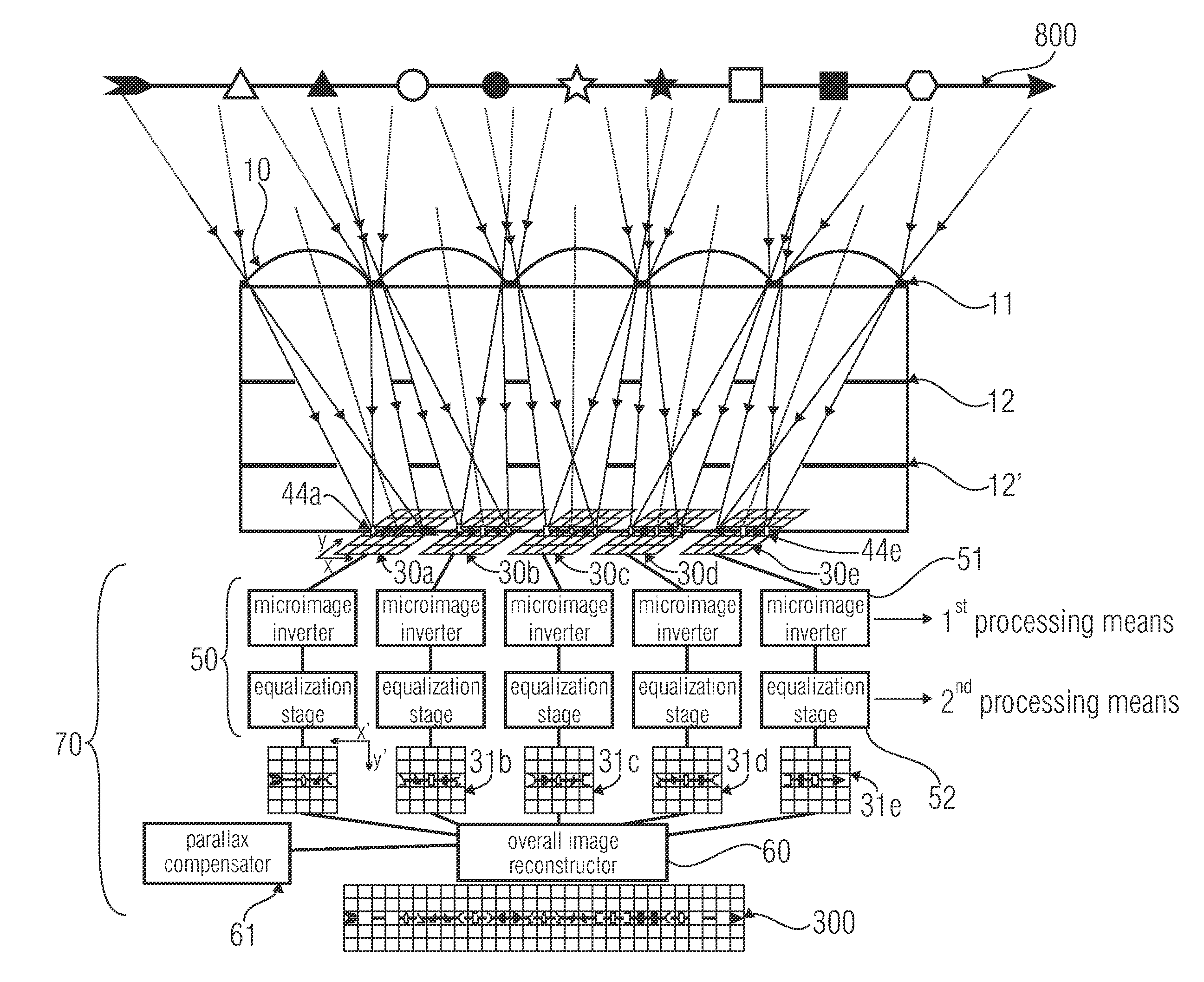
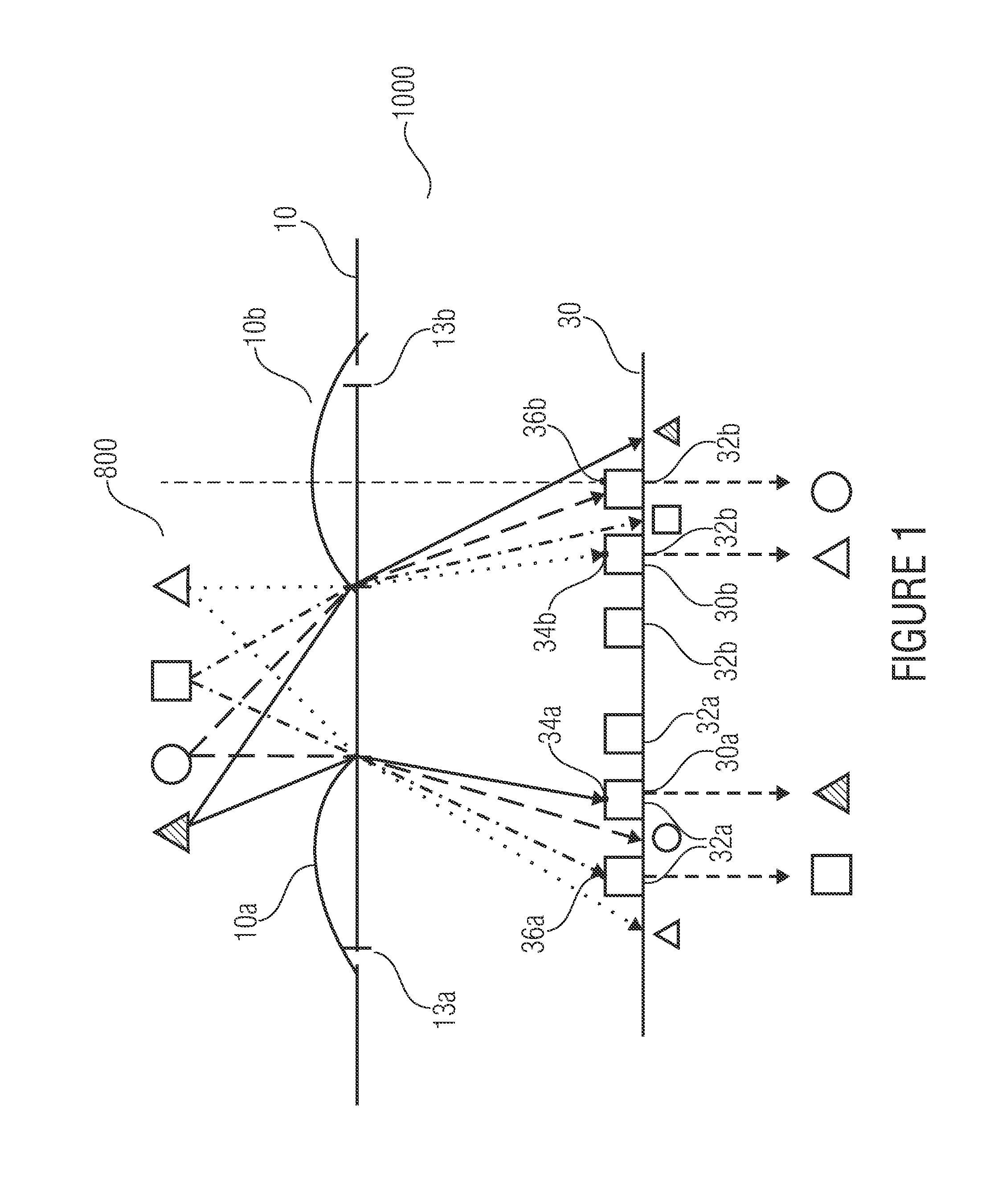
- A device with a micro lens field comprising at least two micro lenses and multiple image detector matrices, where the centers of the image detector matrices are laterally shifted to create overlapping detection areas, allowing for parallel detection of object fields and simple optical components, enabling high image resolution and cost-effective manufacturing using established micro-optical technologies.

Wafer level optics
PatentActiveUS8662765B2
Innovation
- A two-element composite lens architecture is developed for wafer-level cameras, utilizing a wide range of refractive materials and a replication process that includes UV curing, allowing for improved illumination efficiency and simplified manufacturing, enabling the production of compact, high-resolution optical systems with reduced complexity and cost.


Manufacturing Equipment and Infrastructure Investment Analysis
The manufacturing equipment requirements for wafer-level optics and micro-lens arrays differ significantly in terms of capital investment and infrastructure complexity. Wafer-level optics manufacturing demands sophisticated semiconductor fabrication equipment, including advanced lithography systems capable of sub-micron resolution, precision etching tools, and specialized coating deposition systems. These systems typically require investments ranging from $10-50 million per tool, with complete fabrication lines often exceeding $200 million in total equipment costs.
Micro-lens array production utilizes more accessible manufacturing approaches, including precision molding equipment, UV lithography systems, and replication tools. The equipment investment for micro-lens array manufacturing typically ranges from $2-15 million for a complete production line, making it significantly more cost-effective for smaller-scale operations. However, the choice between technologies depends heavily on volume requirements and precision specifications.
Infrastructure considerations reveal additional cost disparities between the two approaches. Wafer-level optics manufacturing requires cleanroom facilities meeting Class 10 or better standards, sophisticated environmental control systems, and extensive utility infrastructure including ultra-pure water systems, specialty gas delivery networks, and high-capacity electrical systems. These infrastructure requirements can add $50-100 million to facility development costs.
Micro-lens array production operates effectively in Class 1000-10000 cleanroom environments with less stringent environmental controls. The reduced infrastructure requirements translate to facility costs of $5-20 million, depending on production scale and automation levels. Additionally, the equipment footprint for micro-lens arrays is typically 60-70% smaller than equivalent wafer-level optics production capacity.
Maintenance and operational costs further differentiate the two technologies. Wafer-level optics equipment requires specialized technical support, expensive consumables, and frequent calibration procedures, resulting in annual operating costs of 15-25% of initial equipment investment. Micro-lens array systems demonstrate lower maintenance complexity with annual operating costs typically ranging 8-15% of equipment value, contributing to improved long-term cost predictability and reduced operational risk for manufacturing organizations.
Supply Chain Risk Assessment for Optical Component Production
The optical component production supply chain faces significant vulnerabilities when comparing wafer-level optics and micro-lens arrays manufacturing approaches. Geographic concentration of specialized manufacturing capabilities creates substantial risk exposure, particularly in Asia-Pacific regions where approximately 70% of precision optical fabrication occurs. Taiwan and South Korea dominate semiconductor-grade wafer processing infrastructure, while specialized micro-lens array production remains concentrated in Germany, Japan, and select facilities in China.
Raw material dependencies present critical bottlenecks for both technologies. High-purity silicon wafers require specialized suppliers with limited global capacity, creating potential shortages during demand spikes. Micro-lens arrays depend on specialized optical polymers and precision glass substrates, with key suppliers concentrated in fewer than ten global facilities. Supply disruptions in either segment can cascade through entire production networks within weeks.
Manufacturing equipment represents another vulnerability layer. Wafer-level optics production requires advanced lithography systems primarily supplied by ASML and a few Japanese manufacturers. These systems have lead times exceeding 18 months and limited service networks. Micro-lens array production equipment, while more distributed among suppliers, still relies on precision molding and replication systems from specialized European manufacturers with similar lead time constraints.
Quality control and testing equipment supply chains add complexity to risk assessment. Both technologies require sophisticated metrology systems for optical performance validation. Key suppliers include Zeiss, KLA-Tencor, and several Japanese precision instrument manufacturers. Equipment failures or supply interruptions can halt production lines indefinitely, as alternative suppliers often require extensive qualification processes.
Logistics vulnerabilities affect both production approaches differently. Wafer-level optics benefit from established semiconductor shipping networks but face contamination risks during transport. Micro-lens arrays require specialized packaging to prevent optical surface damage, limiting carrier options and increasing dependency on specialized logistics providers.
Geopolitical factors increasingly influence supply chain stability. Trade restrictions, export controls, and regional conflicts can rapidly disrupt established supply networks. Both technologies face exposure to policy changes affecting semiconductor equipment exports and rare earth material availability, requiring diversification strategies and alternative sourcing arrangements to maintain production continuity.
Unlock deeper insights with Patsnap Eureka Quick Research — get a full tech report to explore trends and direct your research. Try now!
Generate Your Research Report Instantly with AI Agent
Supercharge your innovation with Patsnap Eureka AI Agent Platform!