Wafer-Level Optics vs Micro-Optical Elements: Cost-Effect Analysis
APR 9, 20269 MIN READ
Generate Your Research Report Instantly with AI Agent
Patsnap Eureka helps you evaluate technical feasibility & market potential.
Wafer-Level Optics Development Background and Objectives
Wafer-level optics emerged in the late 1990s as a revolutionary approach to optical component manufacturing, fundamentally transforming how micro-optical systems are conceived and produced. This technology represents a paradigm shift from traditional discrete optical element assembly to batch fabrication processes that leverage semiconductor manufacturing techniques. The evolution began with the recognition that conventional optical systems faced significant limitations in miniaturization, cost reduction, and mass production scalability.
The historical development of wafer-level optics can be traced through several key phases. Initially, researchers focused on adapting photolithography and etching processes from semiconductor fabrication to create optical structures. Early implementations concentrated on simple diffractive elements and basic refractive surfaces. The technology gained momentum in the 2000s with advances in precision molding, UV-curable materials, and multi-level lithography techniques that enabled more complex optical geometries.
Current technological trends indicate a strong movement toward integration and miniaturization across multiple industries. Consumer electronics demand increasingly compact camera modules with enhanced optical performance, while automotive applications require robust, cost-effective sensing solutions for autonomous driving systems. Medical devices seek miniaturized optical components for endoscopic and diagnostic applications, and telecommunications infrastructure requires high-volume, low-cost optical interconnects.
The primary objective of wafer-level optics development centers on achieving cost-effective mass production of high-quality optical components while maintaining or improving performance compared to traditional micro-optical elements. This involves developing manufacturing processes that can produce thousands of optical elements simultaneously on a single wafer substrate, dramatically reducing per-unit costs through economies of scale.
Technical objectives encompass advancing precision molding techniques to achieve sub-micron accuracy, developing new optical materials with enhanced properties, and creating integrated optical systems that combine multiple functions on single substrates. Performance targets include maintaining optical quality comparable to conventionally manufactured elements while achieving significant cost reductions and enabling new form factors previously impossible with discrete components.
Strategic goals focus on establishing wafer-level optics as the dominant manufacturing approach for high-volume optical applications, particularly in consumer electronics, automotive sensors, and emerging augmented reality systems. The technology aims to enable new product categories through unprecedented miniaturization and cost structures that make optical functionality accessible in previously cost-prohibitive applications.
Market Demand Analysis for Miniaturized Optical Solutions
The global miniaturized optical solutions market is experiencing unprecedented growth driven by the convergence of multiple technological trends and consumer demands. The proliferation of smartphones, tablets, and wearable devices has created an insatiable appetite for compact, high-performance optical components that can deliver superior imaging capabilities while maintaining minimal form factors. This demand extends beyond consumer electronics to encompass automotive applications, where advanced driver assistance systems and autonomous vehicles require sophisticated optical sensors and cameras integrated into increasingly space-constrained environments.
Healthcare and medical device sectors represent another significant growth driver for miniaturized optical solutions. The trend toward minimally invasive surgical procedures and portable diagnostic equipment has intensified the need for ultra-compact optical components that can maintain clinical-grade performance. Endoscopic systems, optical coherence tomography devices, and point-of-care diagnostic instruments all require optical elements that can be manufactured at scale while meeting stringent size and performance requirements.
The industrial automation and Internet of Things markets are generating substantial demand for cost-effective optical sensing solutions. Machine vision systems, barcode scanners, and proximity sensors require optical components that can be produced in high volumes at competitive price points. This market segment particularly values the cost advantages that wafer-level optics can provide over traditional micro-optical elements, especially for applications requiring millions of identical components annually.
Augmented reality and virtual reality applications are emerging as transformative market drivers, demanding optical solutions that can deliver immersive experiences while remaining lightweight and comfortable for extended use. These applications require complex optical systems with multiple elements, making cost-effectiveness a critical factor in determining commercial viability. The ability to integrate multiple optical functions onto a single wafer-level platform presents significant advantages for AR/VR manufacturers seeking to optimize both performance and production costs.
Market capacity analysis reveals that the miniaturized optics sector is transitioning from a niche specialty market to a mainstream technology requirement across diverse industries. The automotive sector alone is projected to drive substantial volume growth as vehicles incorporate increasing numbers of cameras and sensors for safety and autonomous driving features. Similarly, the healthcare sector's shift toward personalized and portable medical devices continues to expand the addressable market for compact optical solutions.
The competitive landscape is increasingly favoring solutions that can achieve optimal cost-performance ratios while maintaining manufacturing scalability. Traditional micro-optical elements face pressure from wafer-level alternatives that can offer superior economies of scale for high-volume applications, while wafer-level optics must demonstrate competitive performance characteristics to capture market share in precision-critical applications.
Current Status and Challenges in WLO vs MOE Technologies
Wafer-Level Optics technology has achieved significant maturity in manufacturing processes, particularly in high-volume consumer electronics applications. Current WLO fabrication leverages semiconductor-grade facilities and established lithographic techniques, enabling precise control over optical element geometries at the wafer scale. Major manufacturers have successfully implemented WLO solutions for smartphone cameras, achieving cost efficiencies through batch processing of hundreds of optical elements simultaneously on single wafers.
However, WLO faces substantial challenges in material limitations and design flexibility. The technology remains constrained by the optical properties of available wafer materials, primarily limiting applications to specific wavelength ranges and optical functions. Thermal management during fabrication processes continues to pose difficulties, particularly for complex multi-layer structures requiring precise alignment and minimal stress-induced deformations.
Micro-Optical Elements technology demonstrates superior versatility in material selection and optical design complexity. Current MOE manufacturing encompasses diverse approaches including precision molding, diamond turning, and advanced replication techniques. This flexibility enables MOE solutions to address specialized applications requiring exotic materials, complex surface profiles, or unique optical characteristics that WLO cannot accommodate.
The primary challenge confronting MOE technology lies in scalability and manufacturing consistency. Individual element fabrication or small-batch processing inherently increases per-unit costs compared to wafer-scale production. Quality control across large production volumes remains problematic, with variations in surface finish and dimensional accuracy affecting optical performance. Additionally, assembly and alignment processes for MOE-based systems typically require more sophisticated handling equipment and longer processing times.
Both technologies face emerging challenges from increasing miniaturization demands and performance requirements. Advanced applications in augmented reality, LiDAR systems, and high-resolution imaging push the boundaries of current manufacturing capabilities. Integration complexity continues to grow as optical systems require tighter tolerances and more sophisticated functionality within increasingly compact form factors.
The competitive landscape reveals a clear technological divide based on application requirements and production volumes. WLO dominates high-volume, standardized applications where cost per unit is paramount, while MOE maintains advantages in specialized, low-to-medium volume applications requiring customized optical solutions or superior performance characteristics.
Current Technical Solutions for Cost-Effective Optics
01 Wafer-level fabrication and batch processing techniques
Wafer-level fabrication enables the simultaneous production of multiple micro-optical elements on a single wafer substrate, significantly reducing manufacturing costs through economies of scale. This approach utilizes semiconductor manufacturing processes and batch processing techniques to create arrays of optical components that can be diced and separated after completion. The method eliminates the need for individual component assembly and alignment, thereby reducing labor costs and improving production efficiency. Advanced lithography and etching processes allow for precise replication of optical structures across the entire wafer surface.- Wafer-level packaging and integration techniques: Wafer-level packaging techniques enable cost-effective manufacturing by processing multiple optical components simultaneously on a single wafer before dicing. This approach reduces assembly costs, improves alignment accuracy, and enables mass production of micro-optical elements. The integration of optical components at the wafer level eliminates individual component handling and reduces material waste, significantly lowering overall production costs while maintaining high precision and quality standards.
- Replication and molding processes for micro-optical elements: Cost-effective manufacturing of micro-optical elements can be achieved through replication techniques such as injection molding, embossing, and casting. These processes allow for high-volume production of optical components with consistent quality at reduced costs compared to traditional grinding and polishing methods. The use of master templates and molds enables rapid reproduction of complex optical surfaces and microstructures, making it economically viable for large-scale production applications.
- Array-based manufacturing and parallel processing: Manufacturing multiple micro-optical elements in array configurations enables parallel processing and significantly reduces per-unit costs. This approach allows simultaneous fabrication, testing, and packaging of numerous optical components on a single substrate. Array-based methods improve throughput, reduce handling requirements, and optimize material utilization, making them particularly cost-effective for applications requiring large quantities of identical or similar optical elements.
- Simplified alignment and assembly methods: Cost reduction in micro-optical systems can be achieved through innovative alignment and assembly techniques that minimize manual intervention and specialized equipment requirements. Self-alignment features, passive alignment structures, and integrated alignment marks enable faster and more reliable assembly processes. These methods reduce labor costs, decrease assembly time, and improve yield rates by eliminating complex active alignment procedures that require expensive equipment and skilled operators.
- Material selection and substrate optimization: Selecting appropriate materials and optimizing substrate properties contributes significantly to cost-effectiveness in wafer-level optics production. The use of cost-efficient optical materials, such as polymers and glass substrates with suitable optical properties, reduces raw material expenses while maintaining performance requirements. Substrate optimization includes selecting appropriate thicknesses, surface treatments, and material compositions that balance optical performance with manufacturing feasibility and cost constraints.
02 Replication and molding technologies for micro-optics
Cost-effective production of micro-optical elements can be achieved through replication techniques such as injection molding, compression molding, and UV-curing processes. These methods allow for high-volume manufacturing by creating master templates that can be replicated thousands of times, dramatically reducing per-unit costs. The replication approach is particularly suitable for polymer-based micro-optical components, enabling rapid production cycles and minimal material waste. This technology supports the creation of complex optical geometries including microlens arrays, diffractive optical elements, and freeform surfaces at significantly lower costs compared to traditional grinding and polishing methods.Expand Specific Solutions03 Integration of optical elements with semiconductor devices
Direct integration of micro-optical elements with semiconductor chips and sensors at the wafer level reduces assembly costs and improves system performance. This approach eliminates the need for separate optical component packaging and alignment procedures, which are typically expensive and time-consuming. Monolithic integration techniques enable the fabrication of optical structures directly on or within semiconductor substrates, creating compact optoelectronic systems with reduced component count. The integration strategy also minimizes optical losses and improves reliability by reducing the number of interfaces and connection points in the optical path.Expand Specific Solutions04 Standardized packaging and modular optical systems
Development of standardized packaging formats and modular optical architectures reduces costs through component interchangeability and simplified assembly processes. Standardization enables the use of common manufacturing equipment and processes across different product lines, reducing tooling costs and inventory requirements. Modular designs allow for flexible system configurations where optical elements can be easily replaced or upgraded without redesigning the entire system. This approach also facilitates automated assembly and testing procedures, further reducing labor costs and improving production throughput.Expand Specific Solutions05 Advanced materials and simplified optical designs
Utilization of cost-effective optical materials and simplified optical designs reduces both material and processing costs while maintaining acceptable performance levels. Novel polymer materials and hybrid glass-polymer compositions offer lower material costs and easier processing compared to traditional optical glasses. Simplified optical architectures that minimize the number of optical surfaces and components reduce manufacturing complexity and assembly requirements. Design optimization techniques enable the achievement of desired optical performance with fewer elements, reducing both material consumption and processing steps. Computational design methods allow for the creation of freeform and aspheric surfaces that can replace multiple conventional optical elements.Expand Specific Solutions
Major Players in WLO and MOE Industry Landscape
The wafer-level optics versus micro-optical elements market represents a rapidly evolving sector within the broader optical semiconductor industry, currently in a growth phase driven by increasing demand for miniaturized imaging solutions across consumer electronics, automotive, and industrial applications. The market demonstrates significant scale potential, with established players like Sony, Canon, and Himax Technologies leading in image sensor integration, while specialized firms such as ams-OSRAM, VisEra Technologies, and Anteryon International focus on advanced micro-optical manufacturing. Technology maturity varies considerably across the competitive landscape, with companies like TSMC and Samsung Display providing foundational semiconductor capabilities, while emerging players including Trusee Technologies and Skyverse Technology develop next-generation optical measurement systems. The cost-effectiveness analysis reveals a bifurcated market where wafer-level approaches offer economies of scale for high-volume applications, particularly evident in Sony's and OmniVision's consumer imaging solutions, while micro-optical elements provide superior performance for specialized applications, as demonstrated by Canon's precision optics and Fraunhofer's research initiatives.
Sony Group Corp.
Technical Solution: Sony has developed advanced wafer-level optics (WLO) technology for mobile camera modules, integrating multiple optical elements directly onto semiconductor wafers during fabrication. Their approach combines wafer-level manufacturing with precision molding techniques to create compact lens systems with reduced assembly costs. Sony's WLO solutions achieve significant miniaturization while maintaining optical performance comparable to traditional discrete lens assemblies. The company has implemented automated wafer-level testing and quality control systems that enable mass production scalability. Their technology particularly excels in smartphone camera applications where space constraints are critical, offering up to 40% reduction in module height compared to conventional micro-optical assemblies.
Strengths: Market leadership in image sensors, established manufacturing infrastructure, strong integration capabilities. Weaknesses: Higher initial tooling costs, limited flexibility for design modifications after wafer processing.
Canon, Inc.
Technical Solution: Canon employs hybrid approach combining wafer-level optics with precision micro-optical elements for high-performance imaging systems. Their technology focuses on wafer-level fabrication of aspherical lens arrays using advanced replication molding processes that achieve sub-micron accuracy. Canon's cost-effectiveness strategy involves batch processing of hundreds of optical elements simultaneously on single wafers, reducing per-unit manufacturing costs by approximately 60% compared to individual lens grinding. The company has developed proprietary materials and coating technologies optimized for wafer-level processing, enabling complex multi-layer optical structures. Their solutions are particularly effective for industrial imaging, medical devices, and high-end consumer electronics where optical quality cannot be compromised.
Strengths: Extensive optical design expertise, advanced manufacturing capabilities, strong IP portfolio in precision optics. Weaknesses: Complex process control requirements, higher material costs for specialized substrates.
Key Patents and Innovations in WLO Manufacturing Processes
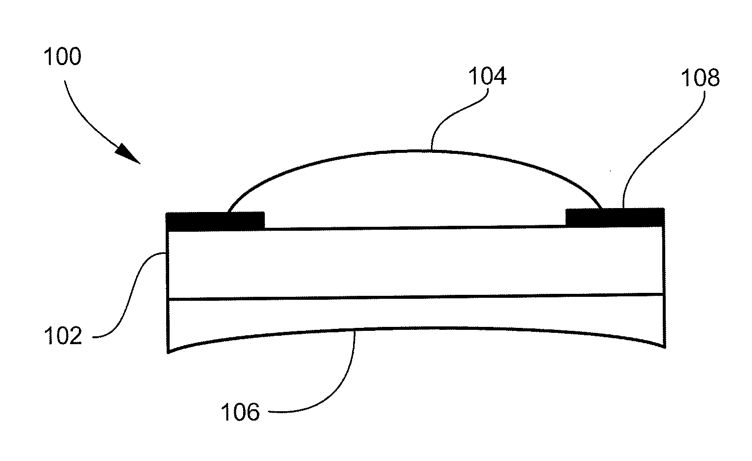
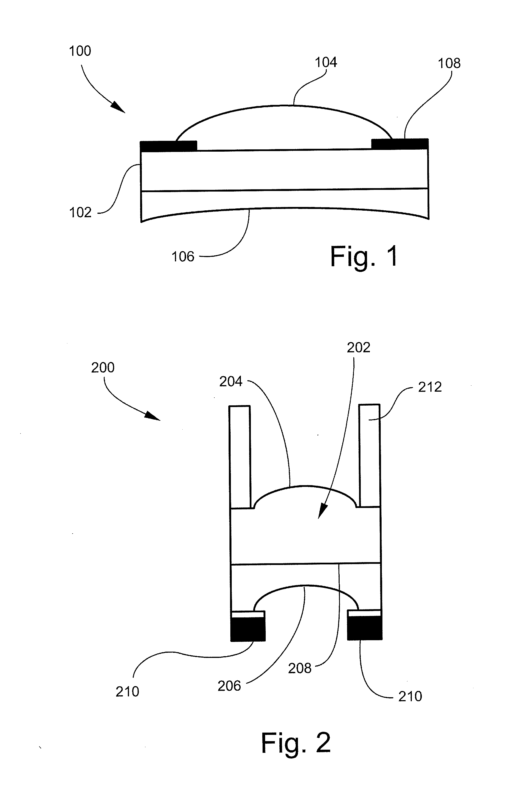
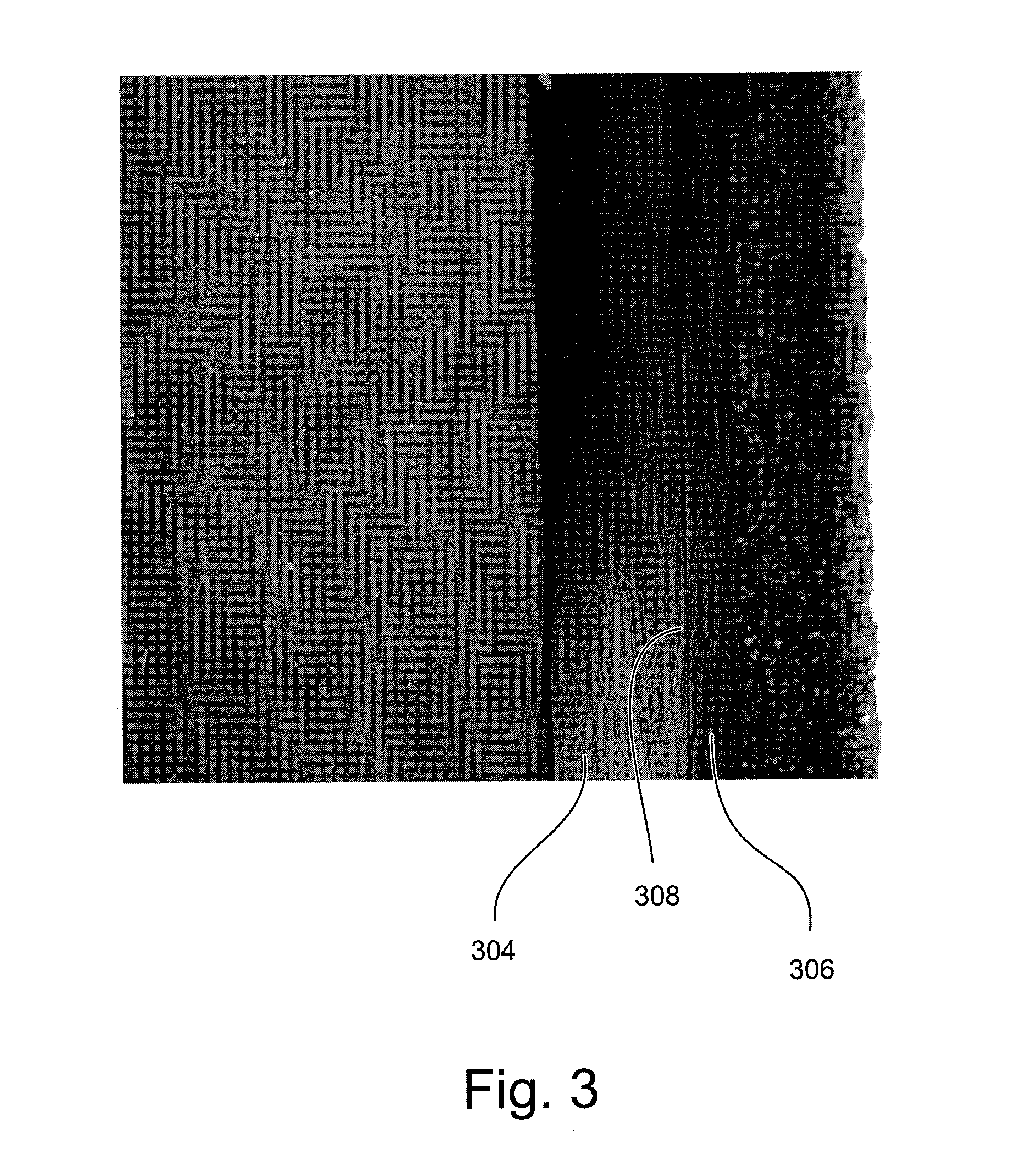
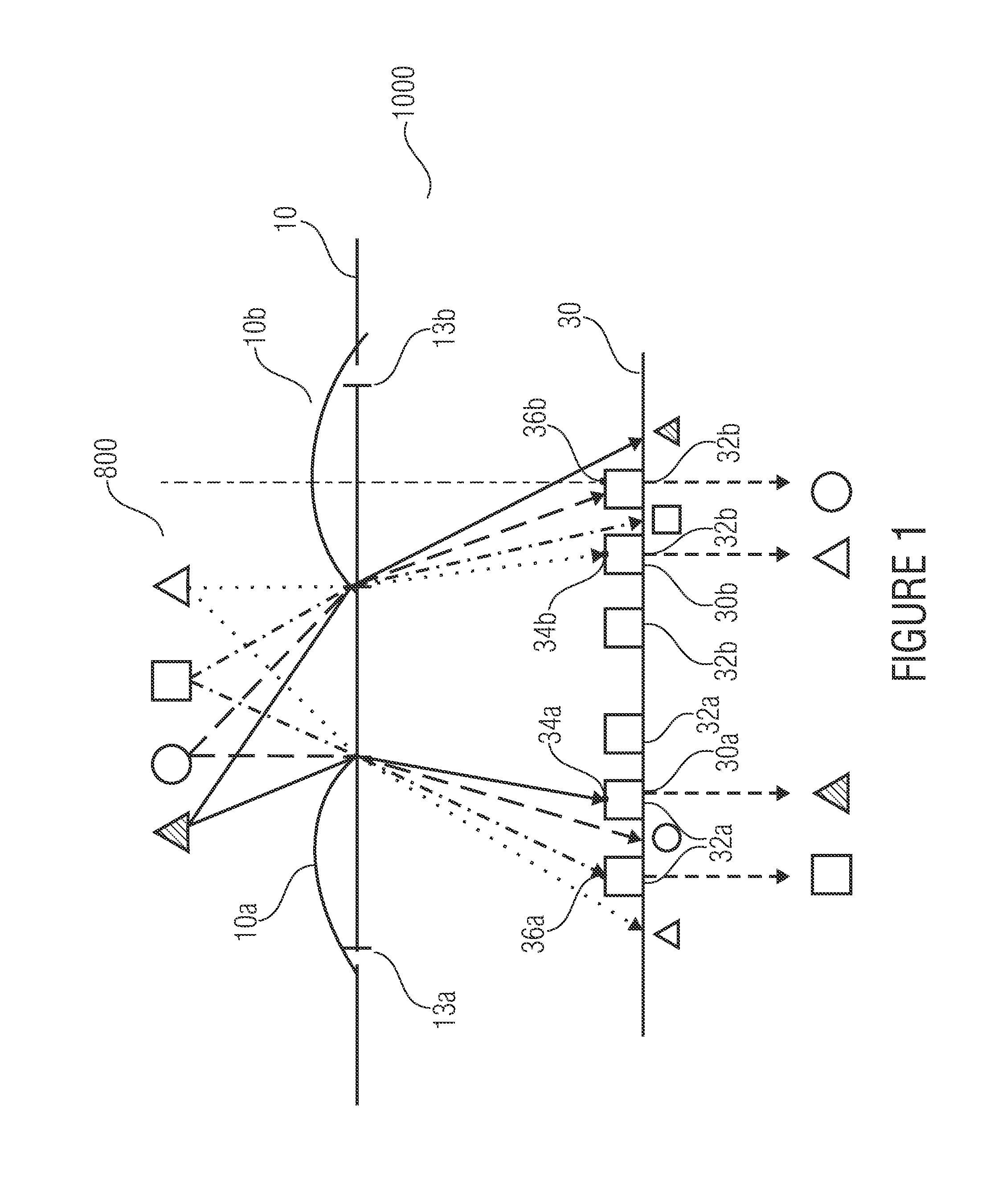
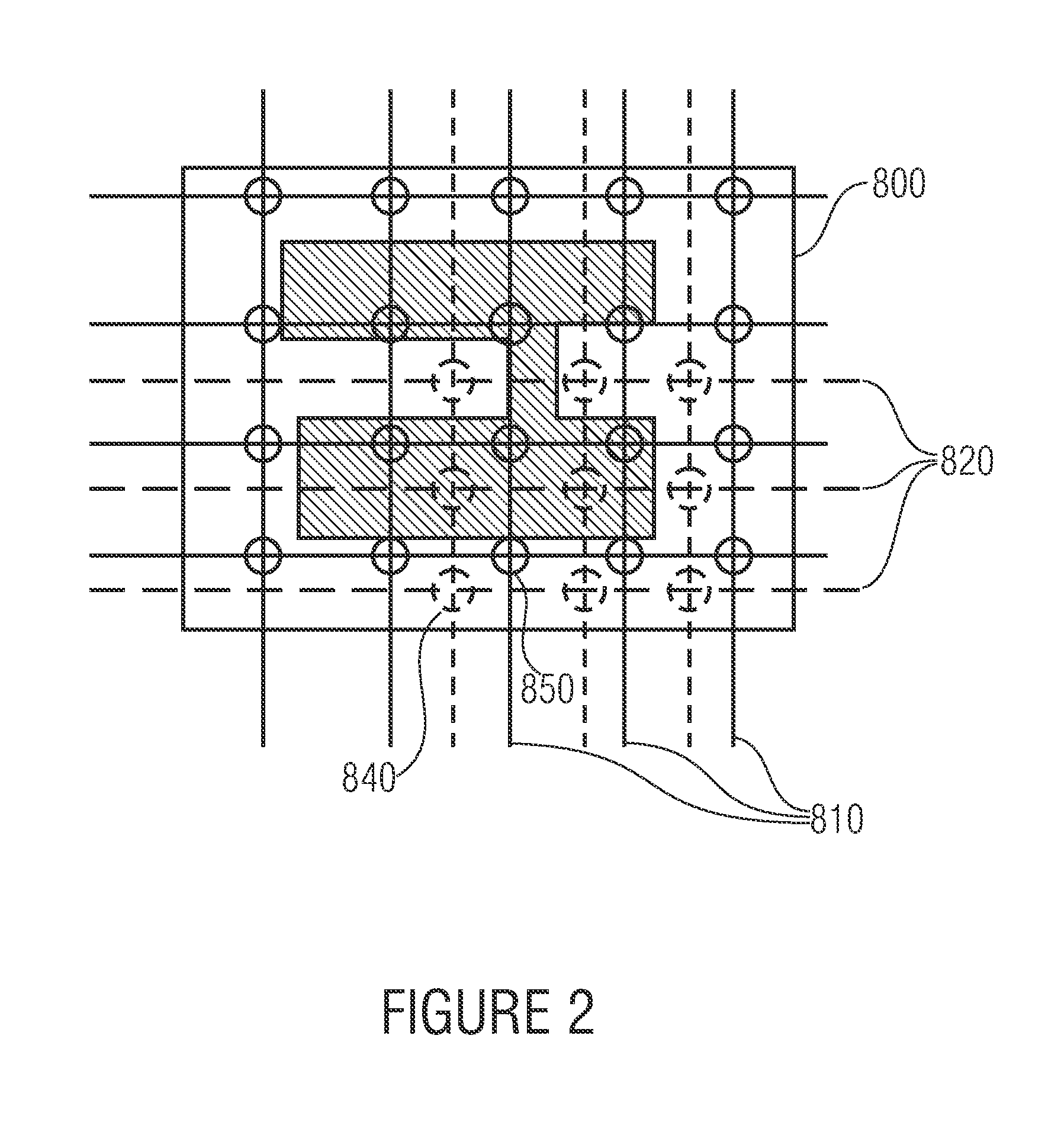
Wafer level optical elements and applications thereof
PatentInactiveUS20110002053A1
Innovation
- Wafer level optical elements are designed without a supporting substrate between optical structures, featuring coupled lens structures with an interface and integrated apertures, allowing for improved optical performance, reduced center thickness, and thermal stability through material matching of lens structures and apertures.

Device, image processing device and method for optical imaging
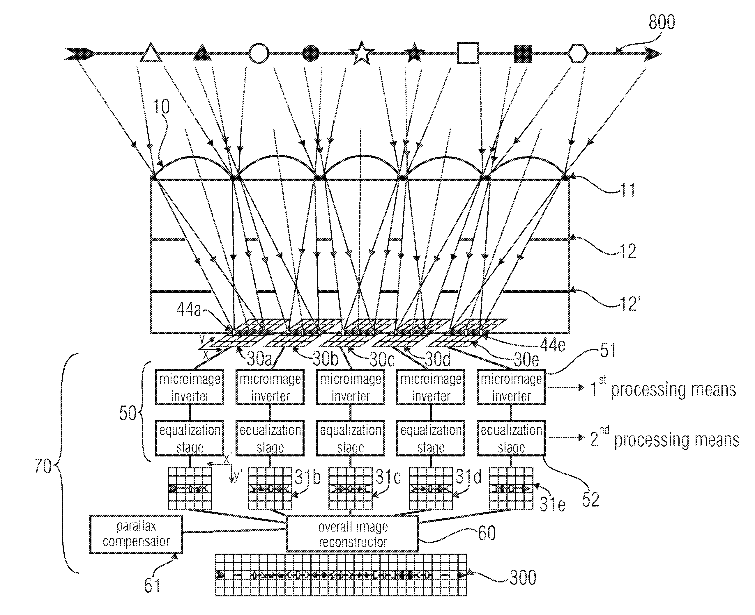
PatentActiveUS20110228142A1
Innovation
- A device with a micro lens field comprising at least two micro lenses and multiple image detector matrices, where the centers of the image detector matrices are laterally shifted to create overlapping detection areas, allowing for parallel detection of object fields and simple optical components, enabling high image resolution and cost-effective manufacturing using established micro-optical technologies.

Manufacturing Equipment and Infrastructure Requirements
The manufacturing infrastructure requirements for wafer-level optics and micro-optical elements differ significantly in terms of equipment sophistication, facility specifications, and capital investment levels. Wafer-level optics manufacturing demands semiconductor-grade cleanroom facilities with Class 10 to Class 100 environments, requiring advanced HVAC systems, particle filtration, and contamination control protocols. The production process necessitates specialized lithography equipment including stepper systems, electron beam writers, and advanced photomask aligners capable of sub-micron precision.
For wafer-level optics fabrication, essential equipment includes plasma etching systems, chemical vapor deposition chambers, and ion beam milling tools. These systems require substantial infrastructure support including high-purity gas delivery networks, ultrapure water systems, and chemical waste management facilities. The equipment typically operates under stringent temperature and vibration control requirements, demanding specialized building foundations and environmental isolation systems.
Micro-optical element manufacturing presents more flexible infrastructure requirements, often accommodating conventional optical manufacturing environments with less stringent cleanliness standards. The production setup typically involves precision molding equipment, diamond turning machines, and conventional optical polishing systems. While still requiring controlled environments, the cleanliness requirements are generally less demanding than semiconductor fabrication standards.
The scalability characteristics differ markedly between these approaches. Wafer-level processing enables batch production of hundreds to thousands of optical elements simultaneously, requiring high-throughput processing equipment but offering superior economies of scale. Conversely, micro-optical element production often involves individual or small-batch processing, requiring more flexible but potentially less capital-intensive equipment configurations.
Infrastructure investment analysis reveals that wafer-level optics facilities typically require initial capital expenditures ranging from $50-200 million for comprehensive production lines, while micro-optical manufacturing setups can be established with $5-20 million investments. However, the throughput capabilities and unit cost advantages of wafer-level processing can justify the higher infrastructure requirements for high-volume applications, making the equipment utilization efficiency a critical factor in determining overall cost-effectiveness.
Quality Control and Yield Optimization Strategies
Quality control and yield optimization represent critical differentiators between wafer-level optics and micro-optical elements manufacturing approaches. The fundamental distinction lies in the inspection and correction methodologies employed at different production stages, directly impacting overall cost-effectiveness and scalability.
Wafer-level optics manufacturing benefits from parallel quality control processes, where entire wafer surfaces undergo simultaneous inspection using advanced metrology systems. This approach enables real-time monitoring of critical parameters such as surface roughness, dimensional accuracy, and optical performance across thousands of elements simultaneously. Statistical process control becomes highly effective when applied to wafer-level production, as variations can be detected and corrected before individual die separation.
The yield optimization strategies for wafer-level optics focus on process uniformity across the substrate. Advanced lithography techniques, combined with precise etching control, ensure consistent feature reproduction across the entire wafer surface. Temperature and pressure uniformity during processing stages becomes paramount, requiring sophisticated equipment calibration and environmental control systems.
Micro-optical elements manufacturing employs different quality control paradigms, typically involving individual component inspection after fabrication. This approach allows for more granular quality assessment but introduces significant time and cost penalties. Each element requires separate measurement cycles, creating bottlenecks in high-volume production scenarios.
Yield optimization for micro-optical elements relies heavily on material selection and processing parameter optimization for individual components. The ability to customize processing conditions for specific optical requirements provides flexibility but reduces overall manufacturing efficiency. Rejection rates tend to be higher due to the discrete nature of quality assessment.
Advanced inspection technologies play crucial roles in both approaches. Interferometric measurement systems, automated optical inspection platforms, and machine learning-based defect detection algorithms are increasingly integrated into production workflows. However, the implementation costs and complexity vary significantly between wafer-level and individual element processing.
The economic implications of quality control strategies become apparent when considering throughput requirements and acceptable defect rates. Wafer-level approaches demonstrate superior cost-effectiveness for high-volume applications, while micro-optical element manufacturing maintains advantages in specialized, low-volume production scenarios where individual component optimization justifies additional processing costs.
Unlock deeper insights with Patsnap Eureka Quick Research — get a full tech report to explore trends and direct your research. Try now!
Generate Your Research Report Instantly with AI Agent
Supercharge your innovation with Patsnap Eureka AI Agent Platform!