
Low-Temperature Polycrystalline Silicon (LTPS) technology is one of the most widely used display backplane technologies in modern smartphones, tablets, laptops, and advanced LCD and OLED panels. Renowned for its faster response times, higher resolution support, and energy efficiency compared to older technologies, LTPS has become essential for delivering sharp visuals and smooth user experiences in high-performance screens.
What is LTPS technology? Eureka Technical Q&A explains that LTPS (Low-Temperature Polycrystalline Silicon) display technology offers faster response times, higher resolution, and better energy efficiency — making it ideal for high-performance smartphones, tablets, and modern display panels.

This article explains what LTPS technology is, how it works, its advantages over other display technologies, its role in modern devices, and the challenges it faces as display innovation continues to evolve.
What Is LTPS Technology?
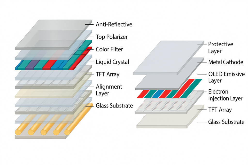
LTPS stands for Low-Temperature Polycrystalline Silicon. It refers to a thin-film transistor (TFT) backplane technology used primarily in high-resolution LCD (Liquid Crystal Display) and OLED (Organic Light-Emitting Diode) panels.
The backplane in a display functions like the control system that turns individual pixels on or off by regulating the electric current flowing through them. LTPS backplanes are manufactured by depositing silicon on a glass substrate at relatively low temperatures (300°C to 650°C) and then crystallizing it into polycrystalline form using laser annealing techniques.
This process results in transistors with significantly higher electron mobility than traditional amorphous silicon (a-Si) backplanes, enabling faster switching speeds, higher pixel densities, and better energy efficiency.
How LTPS Technology Works
LTPS technology uses silicon that has been laser-treated to create polycrystalline structures. The small crystal grains within polycrystalline silicon allow electrons to move much faster than in amorphous silicon.
This improved electron mobility provides several key technical benefits:
- Faster control of individual pixels
- Support for smaller transistors
- Ability to drive higher resolution without increasing power consumption
- Better control of leakage currents, leading to improved efficiency
This makes LTPS especially valuable in devices with compact, high-resolution screens that demand fast response times, such as smartphones, tablets, and laptops.
Benefits of LTPS Technology in Displays
This advanced backplane solution offers clear advantages for both LCD and OLED displays. Many premium devices use it to deliver better performance and energy savings.
Faster Response Time
Its higher electron mobility allows pixels to switch on and off quickly. This reduces motion blur and ensures smoother video playback. Gamers and video lovers benefit most from this feature.
Higher Resolution Displays
It supports smaller transistors, enabling higher pixel density without increasing screen size. This makes it perfect for 4K smartphones, Retina displays, and ultra-sharp visuals.
Better Energy Efficiency
Smaller transistors and reduced leakage current lower power consumption. This extends battery life, a crucial feature for mobile devices.
Thinner and Lighter Screens
Its design needs fewer external components like driver ICs. This helps create thinner display modules and lighter devices.
Higher Brightness and Stronger Contrast
It provides excellent control over pixel lighting. Combined with OLED panels, this results in brighter displays and deeper contrast.
LTPS vs Other Display Backplane Technologies
| Feature | LTPS | a-Si (Amorphous Silicon) | IGZO |
|---|---|---|---|
| Electron Mobility | 100x faster than a-Si | Low | Moderate |
| Resolution Support | Very High | Limited | High |
| Power Efficiency | Excellent | Poor | Very Good |
| Manufacturing Cost | High | Low | Moderate |
| Best Applications | Premium smartphones, high-res displays | Budget and basic LCD displays | Tablets, monitors, OLEDs |
LTPS vs a-Si (Amorphous Silicon)
Amorphous silicon was the traditional material used in early TFT LCD displays but has low electron mobility, making it unsuitable for high-resolution or high-speed screens.
LTPS vs IGZO (Indium Gallium Zinc Oxide)
IGZO offers better energy efficiency than a-Si and can support high resolution but still lags behind LTPS in switching speed and response time.
Applications of LTPS Technology
Low-Temperature Polycrystalline Silicon technology drives many innovations in modern display devices. Its excellent electrical properties enable faster response times, sharper resolution, and lower power consumption than traditional alternatives.
AMLCDs and AMOLED Displays
This technology powers active-matrix liquid-crystal displays (AMLCDs) and active-matrix organic light-emitting diodes (AMOLEDs). It improves refresh rates, enhances image clarity, and delivers a smoother viewing experience.
System-on-Glass Displays
System-on-Glass (SOG) displays use advanced thin-film transistors to integrate circuits directly onto glass panels. This eliminates external drivers, making screens lighter, thinner, and more energy efficient.
Flexible Display Technology
Flexible display applications rely on the material’s high stability and excellent conductivity. It supports the development of foldable smartphones, wearable devices, and sensors in biomedical and robotics fields.
High-Performance Mobile Screens
High-end smartphones and tablets use this technology to deliver brilliant displays with quick response times and high resolution. Devices like iPhone 6s and LG G4 showcase its benefits.
Low-Power Electronics
Engineers use it in low-power devices to balance performance with energy efficiency. Optimizing design geometry helps reduce power consumption in sensor networks, portable electronics, and smart gadgets.
In-Cell Touch Panels
In-Cell touch displays benefit from integrating touch sensors directly into the screen’s pixels. This design improves screen brightness, reduces weight, and lowers energy consumption.
OLED Panels
Organic Light-Emitting Diode (OLED) displays require materials with high electron mobility. This technology meets that need, enabling thinner, more flexible, and more power-efficient OLED screens across multiple devices.
Application Cases
| Product/Project | Technical Outcomes | Application Scenarios |
|---|---|---|
| Five-Mask LTPS CMOS Panel LG Display Co., Ltd. | Reduced manufacturing complexity with five-mask process; Improved contact resistance with selective contact barrier metal formation | Active-matrix liquid-crystal-displays (AMLCDs) requiring high-performance TFTs |
| LTPS Array Substrate Wuhan China Star Optoelectronics Technology Co., Ltd. | Simplified manufacturing process with integrated gate and interlayer insulating layers; Thinner and more cost-effective product | High-resolution displays requiring efficient and cost-effective LTPS substrates |
| Flexible LTPS Sensors Istituto Italiano di Tecnologia | Integration of sensors and signal conditioning circuits on flexible substrates; Excellent electrical characteristics and stability of LTPS TFTs | Biomedical applications, food control, domotics, and robotics requiring flexible and lightweight sensors |
| Self-Reset Ambient-Light Sensor System Seoul National University | Digital ambient-light sensing with time-domain ADC; Simplified analog circuitry for easy integration on glass substrates | LTPS active-matrix displays requiring integrated ambient light sensing capabilities |
| LTPO Display Substrate BOE Technology Group Co., Ltd. | Combined LTPS and oxide TFT technologies; Optimized signal line layout for improved uniformity | High-resolution displays requiring low power consumption and improved display uniformity |
Challenges and Limitations of LTPS Technology
Despite its advantages, LTPS technology faces some important challenges, especially as new display technologies emerge.
High Manufacturing Cost
The complex laser annealing process required to create LTPS increases production costs compared to a-Si or IGZO.
Scalability Issues
LTPS is most suitable for smaller displays (like smartphones) rather than large TV panels due to manufacturing difficulty and cost at larger sizes.
Flexibility Limitations
While LTPS offers excellent electrical performance, it is not as inherently flexible as some newer materials, limiting its use in foldable or curved displays unless combined with special techniques.
The Future of LTPS Technology
This advanced display technology will continue shaping the future of mobile screens, especially in premium devices. Manufacturers rely on it for applications requiring sharp resolution, fast response, and low power consumption.
However, display innovation never stands still. New trends show a growing interest in combining this material with other technologies like IGZO and LTPO (Low-Temperature Polycrystalline Oxide). These combinations help balance performance with energy efficiency and flexibility.
Future Trends to Watch
- Smartphone and wearable makers will widely adopt LTPO backplanes to improve battery life.
- New processing techniques will improve production yield and lower manufacturing costs.
- Micro-LED and next-generation OLED displays will increasingly use this material for better performance.
- Hybrid backplane technologies will support flexible, foldable, or rollable screens in future devices.
As consumer demand grows for thinner, brighter, and longer-lasting displays, this technology will evolve alongside other innovations. The future of displays will depend on blending speed, clarity, durability, and energy savings into one powerful solution.
Conclusion
LTPS technology remains a vital backbone of modern display engineering, enabling faster response times, higher resolution, and better power efficiency in a wide range of devices. While its manufacturing cost limits its use to premium products, LTPS continues to deliver outstanding performance in the competitive display market.
As the demand for high-performance, energy-efficient screens grows across smartphones, laptops, wearables, and beyond, LTPS will continue to evolve — either on its own or in combination with other emerging backplane technologies — shaping the future of display innovation.
FAQs
LTPS stands for Low-Temperature Polycrystalline Silicon — a display backplane technology for driving high-resolution and fast-response screens.
LTPS has much higher electron mobility, allowing faster pixel switching, higher resolution, and lower power consumption.
LTPS is used in both LCD and OLED panels, particularly in high-end smartphones and tablets.
The main drawback is its higher manufacturing cost compared to older technologies like amorphous silicon.
LTPS is expected to remain dominant in premium mobile devices while being integrated with new technologies like LTPO for improved power efficiency and flexibility.
To get detailed scientific explanations of LTPS, try Patsnap Eureka.
