

01 Hot Tech and Product Updates
In this report, there are 2 news articles on the latest developments in the field of Semiconductor Doping – Craft. These articles have been analyzed from 2 sides: the impact of technological innovations and their effects on users. From this analysis, we have summarized the following key points:
Tech Innovations
Band Alignment
The alignment of energy bands in semiconductor materials that is crucial for optimizing the flow of electrons. The yttrium doping helps achieve favorable band alignment, which is essential for efficient electronic devices.
Sub-1 Nanometer Node Chips
Refers to the development of semiconductor chips with features smaller than one nanometer. Ytrium doping is a key enabler in achieving such small scales, which can significantly enhance the power efficiency and performance of the chips.
Carrier Injection Efficiency
The efficiency with which electrical carriers (electrons or holes) are injected from the metal electrode into the semiconductor. Yttrium doping significantly enhances this process, thereby improving the overall device performance.
2D Metallization
The process of converting a two-dimensional semiconductor into a metallic state through doping, which is essential for creating effective ohmic contacts that are critical for the efficient operation of semiconductor devices.
Fermi-Level Pinning Effects
A phenomenon that can limit the performance of semiconductor devices by causing an energy barrier at the interface. The yttrium doping strategy helps mitigate these effects, allowing for better control of the electronic properties at the interface.
Plasma-Deposition-Annealing (PDA) Method
A sophisticated fabrication technique that involves the deposition of yttrium using a plasma process followed by annealing. This method is crucial for achieving the precise doping needed to alter the electronic properties of the 2D semiconductor.
Yttrium Doping
Yttrium doping in molybdenum disulfide (MoS2) is a pivotal innovation that transitions the material from a semiconductor to a metallic state, which is crucial for improving the electrical conductivity and reducing the energy barrier at the contact points in transistors.
Ohmic Contact Technology
Refers to the technology used to create contact points on semiconductors that have negligible resistance and ensure maximum efficiency in current transfer, which is enhanced by the yttrium doping method.
Product Effects
Lower Power Consumption
The enhanced efficiency and reduced leakage currents in transistors achieved through yttrium doping lead to lower power consumption, which is critical for energy-sensitive applications.
High Performance in Large-Scale Integrated Circuits
The overall improvements in transistor performance, scalability, and integration facilitated by yttrium doping contribute to higher performance in large-scale integrated circuits, meeting the demands of advanced computing and electronic devices.
Reduced Contact Resistance
By transforming MoS2 into a metallic state, yttrium doping reduces the contact resistance at the interfaces within the transistor, which is crucial for faster and more reliable semiconductor device performance.
Improved Electrostatic Control and Enhanced ON-state Performance
The atomically thin nature of 2D semiconductors, combined with yttrium doping, allows for superior electrostatic control of the transistor channels, leading to enhanced ON-state performance where the transistor can switch on and off more efficiently.
Facilitated Integration in Electronics
The advancements in doping techniques, particularly the PDA method, facilitate the integration of 2D semiconductors into various electronic devices by ensuring compatibility with existing fabrication technologies.
Achievement of Ultra-Short Channel Ballistic Transistors
The precise control of material properties through yttrium doping allows for the development of ultra-short channel transistors that can operate at ballistic (collision-free) transport levels, enhancing the speed and efficiency of the transistors.
Development of Complementary Symmetrical CMOS Transistors
The ability to create both n-type and p-type ohmic contacts in 2D semiconductors paves the way for the development of complementary symmetrical CMOS transistors, which are fundamental to modern digital circuits.
Recommended News
New yttrium-doping strategy enhances 2D transistors
Liquid crystal-polymer composites switchable windows for radiant energy flow and privacy control
02 Technologies First Made Public
In this section, you will get the latest breakthroughs in four main technical directions of Semiconductor Doping – Craft. These technologies, first made public, represent the cutting-edge innovations and progress in the solar cell industry, showcasing the potential and direction of future developments.
Annealing
| Annealing | View 11 First Tech |
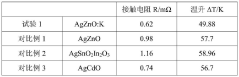
Innovation: Metal ion-doped zinc oxide powder is prepared by solid-state sintering method, then the doped oxide powder and elemental silver powder are mixed through a …
Technical Effect: The invention proposes a method for preparing a low-temperature metal ion-doped silver zinc oxide electrical contact material. The metal ion-doped zinc oxide…
Technical Problem: Existing silver oxide electrical contact materials increase in temperature during service.

A passivated contact structure laminated film, its preparation method and TOPCon battery
Innovation: By performing oxidation pretreatment on the backside of the silicon wafer to form a pretreatment oxide layer, the quality of the tunnel oxide layer can be …
Technical Effect: The preparation method in the present invention can prepare higher quality interface passivation, improve battery efficiency and battery production yield.
Technical Problem: There is a problem of membrane explosion during the preparation process of TOPCon batteries, which results in a narrow process window and also affects the …
Diffusion
| Diffusion | View 8 First Tech |
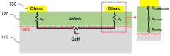
GaN electron device with ohmic electrode and manufacturing method thereof
Abstract: The present invention relates to a gallium nitride-based electronic device having an ohmic electrode and a method of manufacturing the same. A method of manufacturing a gallium nitride-based electronic device with an ohmic electrode …
Silicon carbide epitaxial wafer and preparation method thereof, semiconductor device
Innovation: By introducing etching gases and doping sources between epitaxial layers of different doping types, the doping concentration gradient between epitaxial layer…
Technical Effect: The invention provides a method for preparing silicon carbide epitaxial wafers. By introducing etching gas and doping source between epitaxial layers of …
Technical Problem: In the existing silicon carbide epitaxial wafer growth technology, the interface between epitaxial layers of different doping types is blurred, which affects…
Ion Implantation
| Ion Implantation | View 7 First Tech |
Methods to improve gate polysilicon layer thickness loss
Innovation: By forming a stacked structure on the first gate oxide layer on the storage area, the gate polysilicon layer in the peripheral logic area is effectively …
Technical Effect: The present invention provides a method for improving the thickness loss of the gate polysilicon layer by forming a first gate oxide layer on the storage are…
Technical Problem: During the wet etching process, how to protect the gate polysilicon layer in the peripheral logic area from being damaged to avoid the problem of thinning …
Laterally diffused metal oxide semiconductor device and preparation method thereof
Innovation: Optimizing the performance of a laterally diffused metal oxide semiconductor device is achieved by forming a first gate structure and a first barrier …
Technical Effect: The technical effect of this patent text is to increase the breakdown voltage of the device by forming a second barrier structure above the third region of …
Technical Problem: How to increase the breakdown voltage and maintain low specific on-resistance of laterally diffused metal oxide semiconductor (LDMOS) devices.
03 Technical dynamic report in related fields
This section lists the latest updates from various fields, which will assist you to easily stay informed about the comprehensive progress of the industry and areas you might find interesting.
Wafer – Preparation Crafts
Semiconductor Cleaning
Semiconductor Deposition – Craft
Semiconductor Etching – Craft
Solid State Battery – Manufacturing Processes