
Gate driving unit, gate scanning driver and driving method thereof
A gate drive and driver technology, applied in the direction of instruments, static indicators, etc., can solve the problems of occupation, integration on one side of the substrate, large display substrate area, etc.
Patent Information
- Authority / Receiving Office
- CN · China
- Patent Type
- Patents(China)
- Current Assignee / Owner
- Publication Date
- 2016-03-02
Smart Images
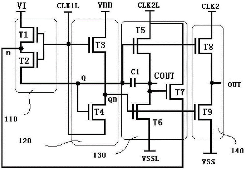
Figure 1 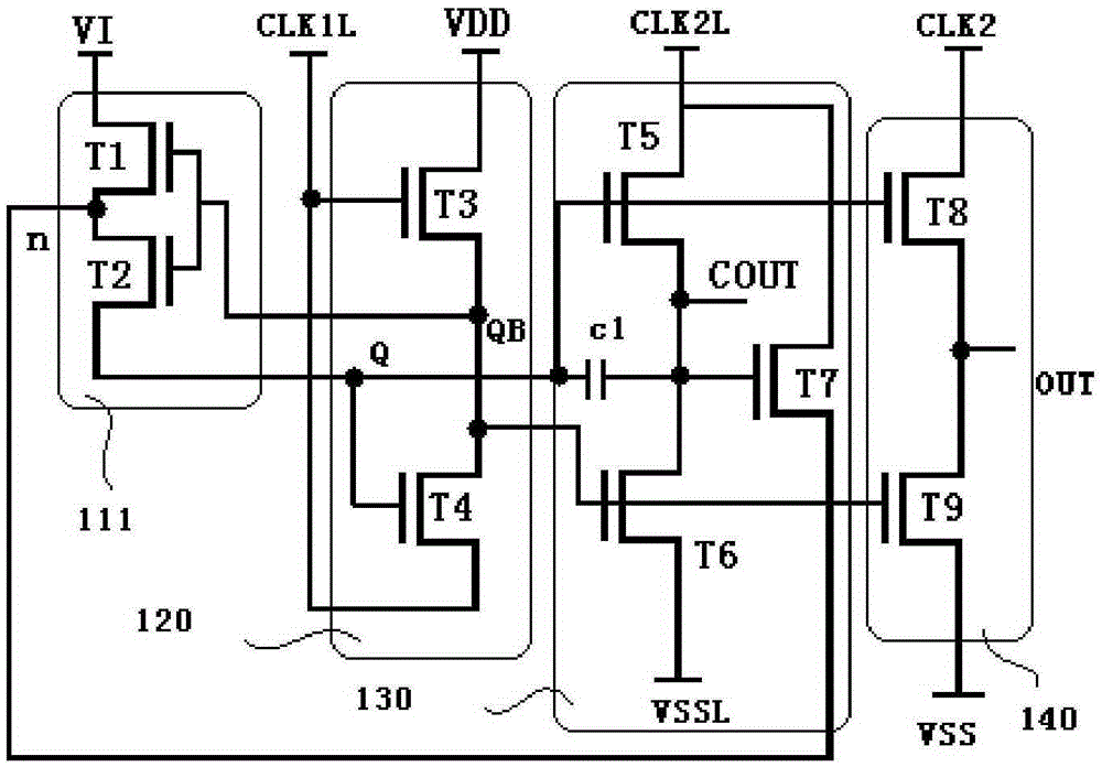
Figure 2 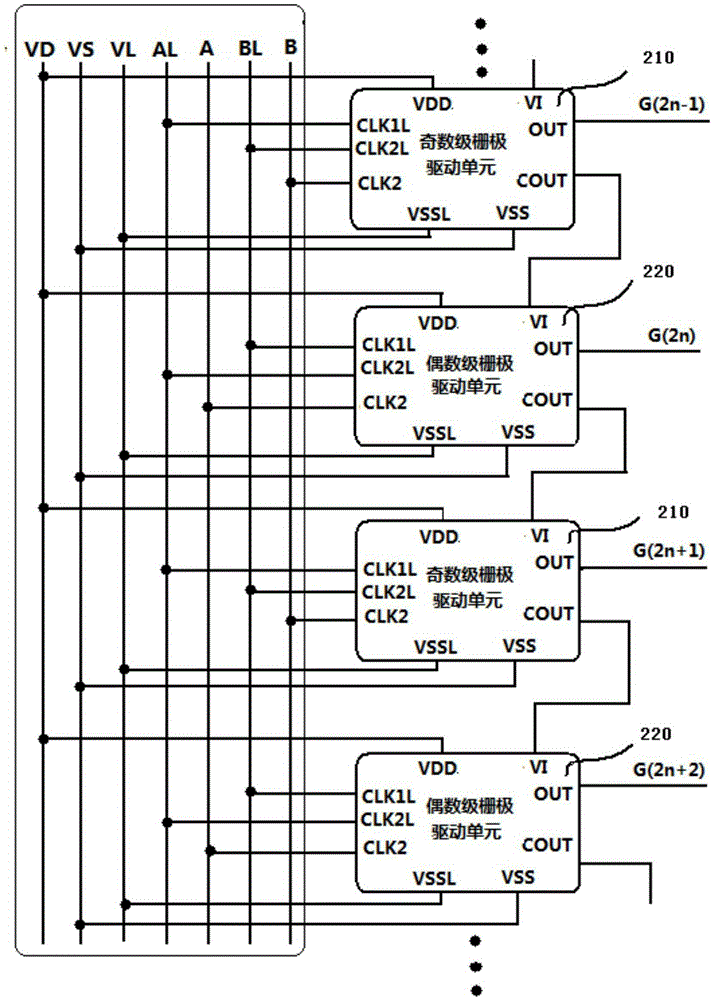
Figure 3
Abstract
Description
technical field
[0001] The invention relates to the technical field of gate scan driving of an organic light emitting diode display, in particular to a gate drive unit, a gate scan driver and a driving method thereof. Background technique
[0002] Active matrix organic light emitting diode (ActiveMatrixOrganicLightEmittingDiode, AMOLED) display is a new type of display that has developed rapidly in recent years. The early AMOLED display gate row scanning driver followed the LCD driving method, and pressed a special driver chip on the glass substrate to drive the pixel circuit through the COG process. In recent years, due to the development of FPD technology, integrated gate drive technology has attracted great interest in the industry. Using the integrated gate scanning driver to drive the gate of the display pixel circuit can reduce the use of the driver chip, reduce the production cost, and can also reduce the loss of signal transmission and improve the display quality. ...
Examples
Embodiment 1
[0069] Such as figure 1 As shown, a gate drive unit includes an information collection module 110, an internal inverter module 120, a first signal output module 130 and a second signal output module 140;
[0070] The signal acquisition module 110 is composed of a first transistor T1 and a second transistor T2, the drain of the first transistor T1 serves as the signal acquisition port VI of the gate drive unit,
[0071] The source of the first transistor T1 is connected to the drain of the second transistor T2; the source of the second transistor T2 outputs the acquisition signal Q;
[0072] The gate of the first transistor T1 is connected to the gate of the second transistor T1 as the first clock input port CLK1L of the gate drive unit;
[0073] The internal inverter module 120 is composed of a third transistor T3 and a fourth transistor T4, the drain of the third transistor T3 is the first power input port VDD,
[0074] The gate of the third transistor T3 is connected to th...
Embodiment 2
[0123] In this embodiment, if figure 2 As shown, the gate of the first transistor T1 in the signal acquisition module 111 is connected to the gate of the second transistor T2 and then connected to the output terminal QB of the internal inverter module 120 ; other features are the same as those in the first embodiment.