
An all-dielectric absorber based on graphene and Dirac semimetal
A semi-metal, wave absorber technology, applied in the field of terahertz metamaterial wave absorption, can solve the problems of small adjustment range, fragile and easy to break, affecting device stability, etc., and achieves wide tunable range, high absorption efficiency, overall Stable performance
Patent Information
- Authority / Receiving Office
- CN · China
- Patent Type
- Patents(China)
- Current Assignee / Owner
- Publication Date
- 2022-03-15
Smart Images
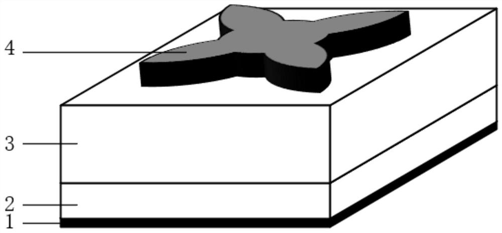
Figure 1 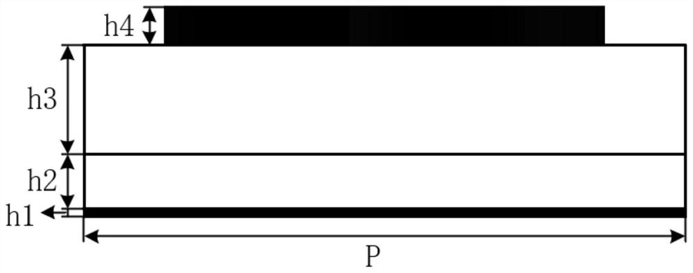
Figure 2 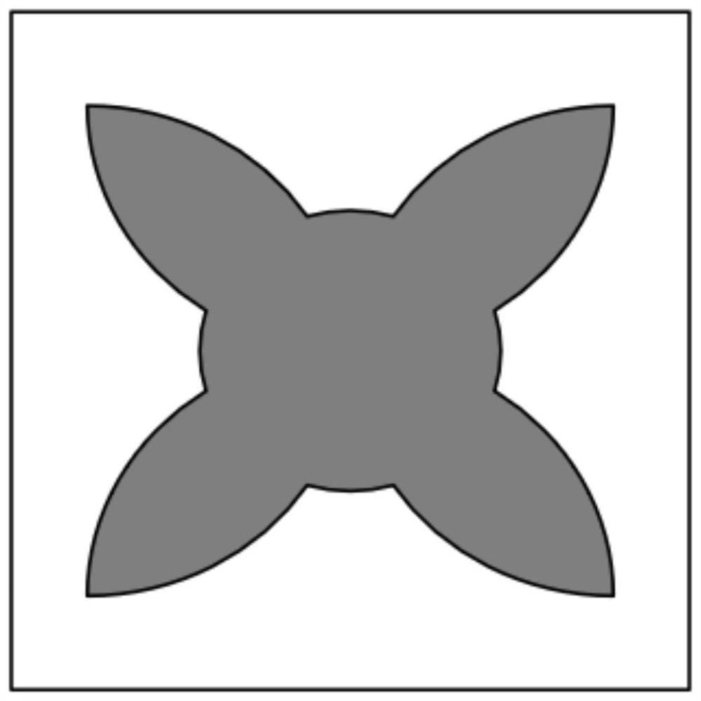
Figure 3
Abstract
Description
technical field
[0001] The invention relates to an all-dielectric wave absorber based on graphene and Dirac semimetal, belonging to the field of terahertz metamaterial wave absorption. Background technique
[0002] A wave absorber is a device that can effectively absorb electromagnetic waves and prevent them from being reflected and transmitted. Electromagnetic waves do not disappear out of thin air, but are converted into other forms of energy inside the wave absorber for consumption. When this property is applied in the military field, it can absorb the electromagnetic wave signal sent by the radar, so that the aircraft has a "stealth" function. Utilizing the high absorption rate of electromagnetic waves, it can also be used in the fields of high-fidelity imaging and thermal detection.
[0003] Existing metamaterial absorbers for terahertz waves usually use a metal thin film as a reflective layer, a middle dielectric layer, and a patterned metamaterial on top. The invent...
Examples
Embodiment 1
[0020] A kind of all-dielectric wave absorber based on graphene and Dirac semimetal, comprising the following steps:
[0021] Such as figure 1 As shown, the absorber comprises a graphene layer (1), a dielectric layer (2) (3) and a Dirac semimetal (4), and the graphene layer (1) is single-layer graphene. Single-layer graphene and Dirac semimetals can receive external excitations to achieve their own Fermi level tuning, thereby enabling tunable absorption frequencies.
[0022] When the terahertz wave is incident on the absorber, the graphene surface plasmon resonance will be excited at the interface between graphene and silicon dioxide, and a strong electric field will be generated here to achieve strong absorption of electromagnetic waves. In the terahertz band, the imaginary part of the conductivity of graphene is greater than zero, showing the properties of a metal, so the energy will not be transmitted, but will only be absorbed or reflected inside the device. Combined wit...