
Solid-state imaging device, method of manufacturing the same, and camera
a solid-state imaging and manufacturing method technology, applied in the field of solid-state imaging devices, can solve the problems of reducing sensitivity, increasing color-mixing, and insufficient light collected by the on-chip microlens, and achieves the effects of suppressing color-mixing, improving sensitivity, and high image quality
Patent Information
- Authority / Receiving Office
- US · United States
- Patent Type
- Patents(United States)
- Current Assignee / Owner
- Publication Date
- 2013-03-12
- Estimated Expiration
- Not applicable · inactive patent
Smart Images
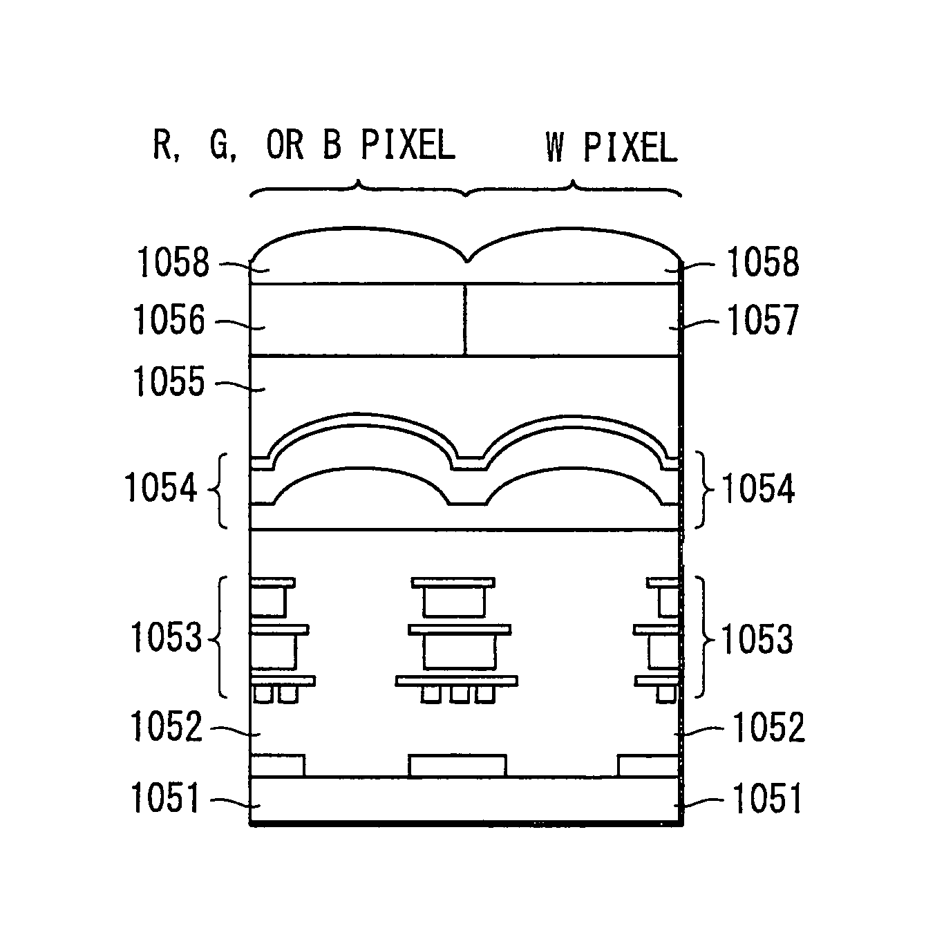
Figure 1 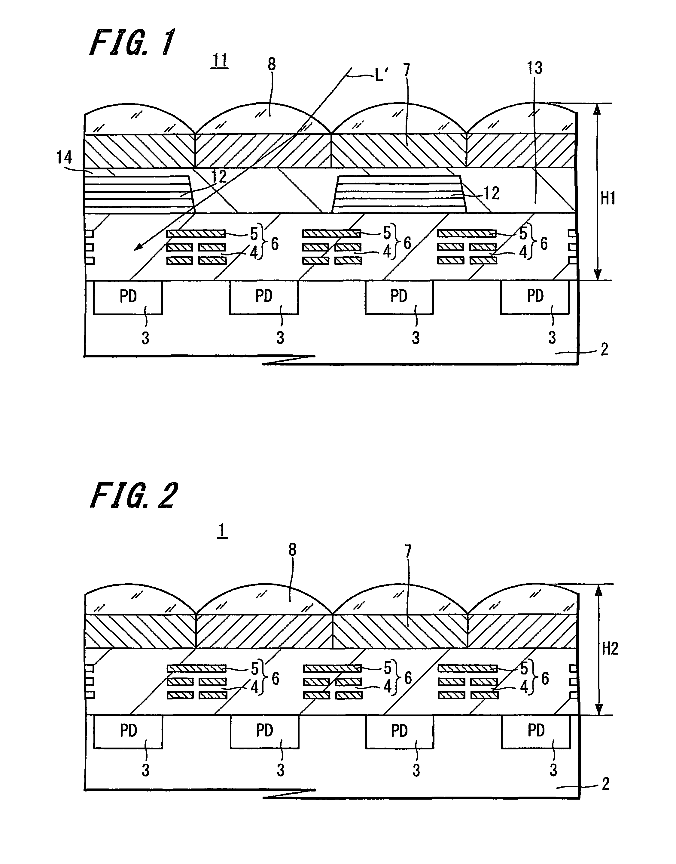
Figure 2 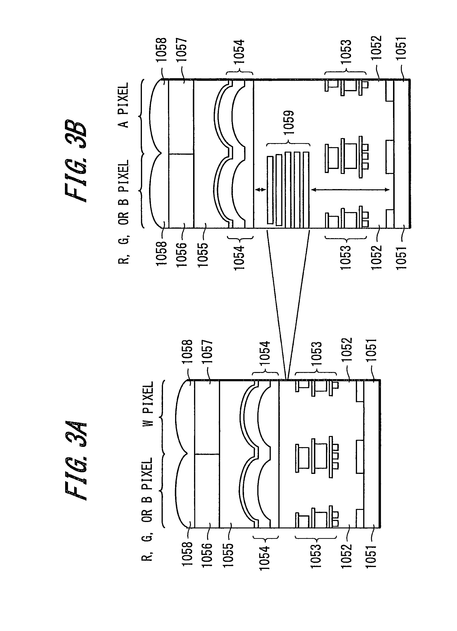
Figure 3
Abstract
Description
CROSS REFERENCES TO RELATED APPLICATIONS
[0001] The present invention contains subject matter related to Japanese Patent Application JP 2007-316280 filed on Dec. 6, 2007 and Japanese Patent Application JP 2008-113016 filed on Apr. 23, 2008, in the Japanese Patent Office respectively, the entire contents of which being incorporated herein by reference.BACKGROUND OF THE INVENTION
[0002] 1. Field of the Invention
[0003] The present invention relates to a solid-state imaging device, for example a MOS image sensor, a method of manufacturing the same, and a camera using such a solid-state imaging device.
[0004] 2. Description of the Related Art
[0005] Solid-state imaging devices can be roughly classified into charge transfer solid-state imaging devices typified by CCD image sensors and amplified solid-state imaging devices typified by CMOS image sensors. In comparison with the CMOS image sensor, the CCD image sensor may need a power supply voltage higher than that of the CMOS image sensor, because ...
Examples
first embodiment
[0122]Next, FIG. 7 illustrates a cross-sectional structure of main parts of a CMOS solid-state imaging device according to the present invention. In order to describe an embodiment of the present invention to be understandable, a pixel is represented only by a photodiode (PD) 31 and schematically described while omitting pixel transistors. The same will be applied to each of other embodiments described later.
[0123]As shown in FIG. 7, a CMOS solid-state imaging device 71 according to the first embodiment includes a plurality of pixels 22, each having the photodiode (PD) 31, arranged in a two-dimensional array on the principal surface of a semiconductor substrate 100. In addition, a plurality of wiring layers 55 are formed on the semiconductor substrate 100 through an insulating interlayer 53. In this example, three layered lines 54 [541, 542, and 543] form the plurality of wiring layers 55. An inner-layer lens 72 is formed corresponding to the respective pixels 22 above the plurality...
second embodiment
[0138]FIG. 11 illustrates a CMOS solid-state imaging device according to the present invention.
[0139]In a CMOS solid-state imaging device 77 of the present embodiment, a buried layer for filling between optical inner filer layers 62 and a planarizing layer are integrally formed with an organic film 81. Here, other structural components are similar to those in FIG. 7 as described above. Therefore, the same structural components in FIG. 11 are designated by the same reference numerals of the corresponding components in FIG. 7 and their duplicate descriptions will be omitted.
[0140]In the CMOS solid-state imaging device 77 of the second embodiment, the organic film 81 filling space between the adjacent optical inner filter layers 62 can also function as a planarizing layer on the layers 62. Thus, it leads to a reduction in number of manufacturing steps and a reduction in distance between the light-receiving surface and the on-chip microlens or a reduction in layer thickness, as well as ...
third embodiment
[0141]FIG. 12 illustrates a CMOS solid-state imaging device according to the present invention. In a CMOS solid-state imaging device 78 of the present embodiment, optical inner filter layers 62 have a lens shape copied from the lens shape of the corresponding inner-layer lens 72. In other words, an insulating interlayer 53, an upwardly-convex first interlayer film 73, and a second interlayer film 74 extending along the upper surface of the first interlayer film 73 form the inner-layer lens 72. In addition, the lens-shaped optical inner filter layer 62 is formed on the second interlayer film 74. Other structural components are the same as those represented in FIG. 7 as described above. Thus, these structural components in FIG. 12 are designated by the same reference numerals of the corresponding components in FIG. 7 and their duplicate descriptions will be omitted.
[0142]As described above, in the CMOS solid-state imaging device 78 according to the third embodiment, each of the optica...