
Electro-optical device, method of manufacturing electro-optical device, and electronic apparatus
a manufacturing method and electrooptical technology, applied in the field of electrooptical devices, can solve the problems of difficult to sufficiently suppress the temperature rise of the element substrate, the electro-optical device's life reduction, and the malfunction or the reduction of life, etc., to achieve the effect of efficient release of the heat of the light-transmitting cover
Patent Information
- Authority / Receiving Office
- US · United States
- Patent Type
- Patents(United States)
- Current Assignee / Owner
- Publication Date
- 2016-10-11
Smart Images
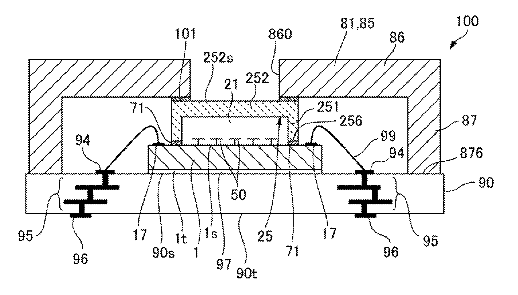
Figure 1 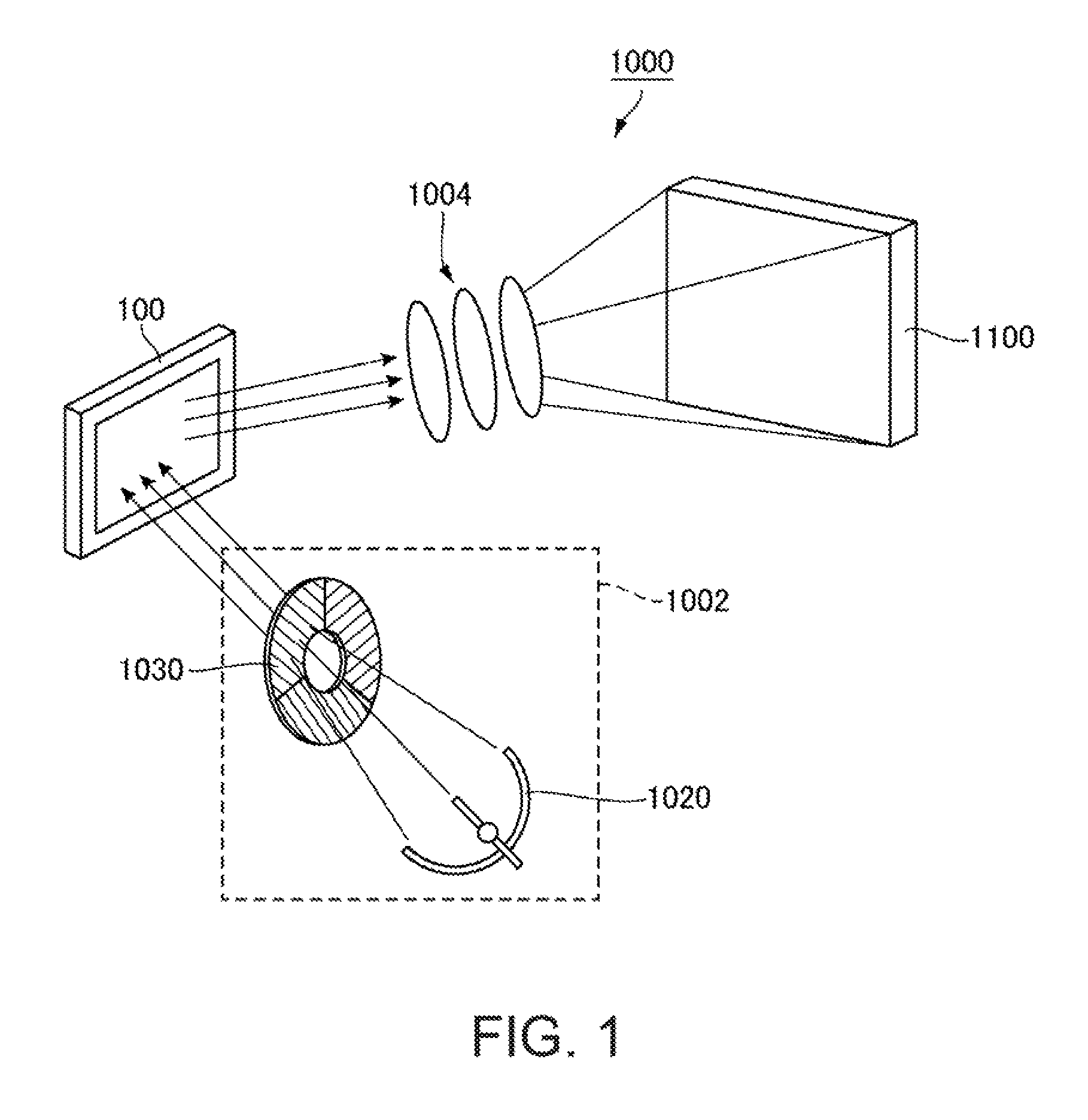
Figure 2 
Figure 3
Abstract
Description
[0001] The entire disclosure of Japanese Patent Application No.2015-065935, filed Mar. 27, 2015 is expressly incorporated by reference herein.BACKGROUND
[0002] 1. Technical Field
[0003] The present invention relates to a method of manufacturing an electro-optical device including a mirror, an electro-optical device, and an electronic apparatus.
[0004] 2. Related Art
[0005] As an electronic apparatus, there has been known, for example, a projective display apparatus that displays an image on a screen by modulating light emitted from a light source by a plurality of mirrors (micromirrors) of an electro-optical device called a digital mirror device (DMD) and then enlargedly projecting the modulated light by a projection optical system. For example, the electro-optical device used in the projective display apparatus includes an element substrate 1 provided with mirrors 50 on one surface 1s, spacers 28 adhering to the one surface 1s of the element substrate 1 so as to surround the mirrors 50 in p...
Examples
embodiment 1
Projective Display Apparatus as Electronic Apparatus
[0049]FIG. 1 is a schematic diagram showing an optical system of a projective display apparatus as an electronic apparatus to which the invention is applied. A projective display apparatus 1000 shown in FIG. 1 includes a light source unit 1002, an electro-optical device 100 that modulates light emitted from the light source unit 1002 according to image information, and a projection optical system 1004 that projects light modulated in the electro-optical device 100 as a projection image onto a projected object 1100 such as a screen. The light source unit 1002 includes a light source 1020, and a color filter 1030. The light source 1020 emits white light, the color filter 1030 emits color light beams with rotation, and the electro-optical device 100 modules incident light at a timing synchronized with the rotation of the color filter 1030. Instead of the color filter 1030, a fluorescent substrate that converts the light emitted from t...
embodiment 2
[0079]FIG. 8 is a sectional view of an electro-optical device 100 according to Embodiment 2 of the invention. FIGS. 9A to 9D are process sectional views showing a method of manufacturing the electro-optical device 100 according to Embodiment 2 of the invention. FIGS. 10A to 10C are process sectional views showing a process of mounting an element substrate 1 on a substrate 90 in the method of manufacturing the electro-optical device 100 according to Embodiment 2 of the invention. Since a basic configuration of the present embodiment is the same as that of Embodiment 1, common portions will be assigned the same reference numerals, and thus, the description thereof will be omitted.
[0080]Similarly to Embodiment 1, as shown in FIG. 8, in the electro-optical device 100 of the present embodiment, the element substrate 1 in which a plurality of mirrors 50 is formed on one surface 1s is mounted on a mounting surface 90s of the substrate 90 made from a ceramic substrate through an adhesive la...
embodiment 3
[0097]FIG. 12 is a sectional view of an electro-optical device 100 according to Embodiment 3 of the invention. FIGS. 13A and 13B are process sectional views showing a method of manufacturing the electro-optical device 100 according to Embodiment 3 of the invention. FIGS. 14A to 14C are process sectional views showing a process of mounting an element substrate 1 on a substrate 90 in the electro-optical device 100 according to Embodiment 3 of the invention. Since a basic configuration of the present embodiment is the same as that of Embodiment 1, common portions will be assigned the same reference numerals, and thus, the description thereof will be omitted.
[0098]Similarly to Embodiment 1, as shown in FIG. 12, in the electro-optical device 100 of the present embodiment, one surface 1s of the element substrate 1 in which a plurality of mirrors 50 is formed on one surface 1s is sealed by a light-transmitting cover 25. The element substrate 1 is mounted on a mounting surface 90s of the su...