

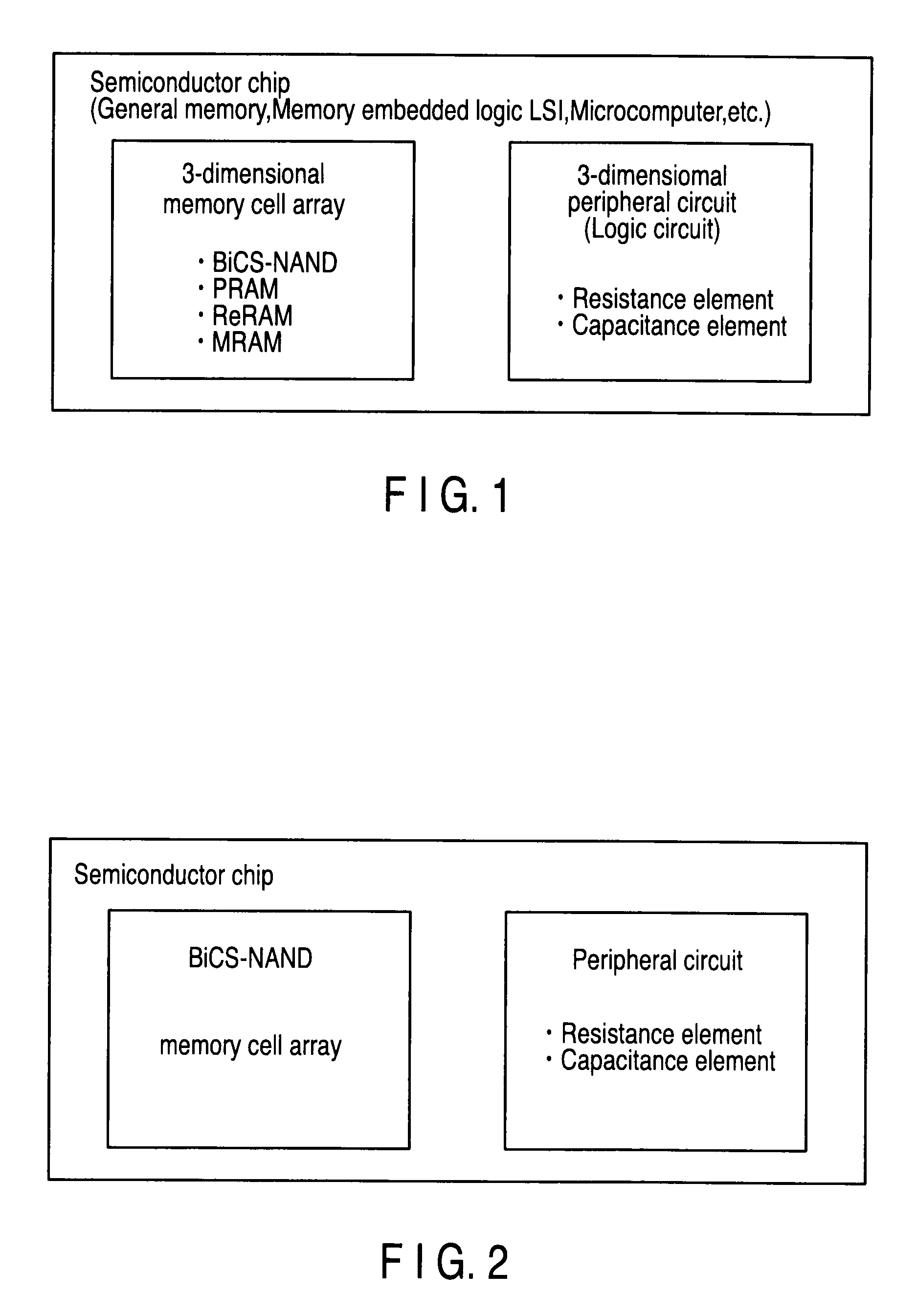
3D DRAM vs BiCS FLASH: Cost Effectiveness
APR 15, 20268 MIN READ
Generate Your Research Report Instantly with AI Agent
PatSnap Eureka helps you evaluate technical feasibility & market potential.
3D DRAM vs BiCS FLASH Cost Analysis Background and Goals
The semiconductor memory industry has reached a critical inflection point where traditional scaling approaches face fundamental physical and economic limitations. As Moore's Law encounters increasing challenges in planar architectures, the industry has pivoted toward three-dimensional memory structures to maintain performance improvements while managing manufacturing costs. This transition has sparked intense debate regarding the optimal balance between performance, density, and cost-effectiveness in next-generation memory solutions.
3D DRAM technology represents an evolutionary leap from conventional planar DRAM architectures, promising to deliver higher memory densities while potentially reducing per-bit costs through vertical scaling. By stacking memory cells in multiple layers, 3D DRAM aims to overcome the area constraints that have historically driven up manufacturing expenses in advanced process nodes. This approach leverages proven DRAM cell physics while introducing novel architectural innovations to address the unique challenges of three-dimensional integration.
BiCS FLASH technology, pioneered by Toshiba and subsequently adopted across the industry, has already demonstrated commercial viability in the NAND flash memory market. The Bit Cost Scalable architecture utilizes vertical charge trap flash cells arranged in a three-dimensional array, enabling significant density improvements over planar NAND while maintaining competitive manufacturing costs. The technology has evolved through multiple generations, with current implementations achieving over 100 layers and continuing to push the boundaries of vertical integration.
The fundamental objective of this cost-effectiveness analysis centers on establishing a comprehensive framework for evaluating the economic viability of 3D DRAM versus BiCS FLASH technologies across multiple application domains. This evaluation must consider not only the direct manufacturing costs but also the total cost of ownership implications for system designers and end users.
Key analytical goals include quantifying the manufacturing cost structures for both technologies, assessing their respective scaling trajectories, and identifying the break-even points where each technology offers superior economic value. The analysis will examine wafer-level costs, yield considerations, packaging requirements, and system-level integration expenses to provide a holistic view of the cost landscape.
Additionally, this study aims to project future cost evolution scenarios based on technology roadmaps, manufacturing learning curves, and anticipated market adoption patterns. Understanding these dynamics is crucial for strategic decision-making in memory technology investments and product development initiatives.
Market Demand for Cost-Effective 3D Memory Solutions
The global memory market is experiencing unprecedented demand driven by the exponential growth of data-intensive applications across multiple sectors. Cloud computing infrastructure, artificial intelligence workloads, and edge computing deployments require increasingly sophisticated memory solutions that balance performance with economic viability. Enterprise data centers are particularly focused on optimizing total cost of ownership while maintaining the storage density and access speeds necessary for modern computational workloads.
Mobile device manufacturers face mounting pressure to deliver enhanced user experiences while managing bill-of-materials costs. The proliferation of 5G networks, augmented reality applications, and high-resolution multimedia content has created substantial demand for memory solutions that can handle larger data volumes without proportionally increasing device costs. Consumer electronics manufacturers are actively seeking memory technologies that enable feature differentiation while maintaining competitive pricing structures.
The automotive industry represents an emerging high-growth segment for cost-effective 3D memory solutions. Advanced driver assistance systems, autonomous vehicle platforms, and connected car technologies require reliable, high-capacity storage that can operate under challenging environmental conditions. Automotive manufacturers prioritize long-term cost predictability and supply chain stability, making cost-effectiveness a critical selection criterion for memory technologies.
Industrial Internet of Things applications are driving demand for memory solutions that combine durability with economic efficiency. Manufacturing automation, smart city infrastructure, and industrial monitoring systems require memory technologies capable of handling continuous data logging and real-time processing while maintaining operational cost targets. These applications often involve large-scale deployments where per-unit memory costs significantly impact overall project economics.
Hyperscale cloud service providers are increasingly evaluating memory technologies based on performance-per-dollar metrics rather than absolute performance specifications. The shift toward software-defined infrastructure and containerized applications has created opportunities for memory solutions that optimize cost-effectiveness across diverse workload patterns. These providers require memory technologies that can scale economically while supporting the varied performance requirements of their customer base.
The growing emphasis on edge computing is creating new market segments where cost-effective 3D memory solutions can provide competitive advantages. Edge deployments often operate under strict cost constraints while requiring sufficient storage capacity and performance for local data processing and caching applications.
Current Cost Structure and Manufacturing Challenges
The cost structure of 3D DRAM and BiCS FLASH technologies reveals fundamental differences in manufacturing complexity and economic viability. 3D DRAM manufacturing requires sophisticated process control due to the need for maintaining electrical characteristics across multiple vertical layers, typically ranging from 8 to 16 layers in current implementations. The fabrication process involves complex capacitor formation and precise channel etching, demanding advanced lithography equipment and specialized materials that significantly increase wafer processing costs.
BiCS FLASH technology, while also utilizing 3D architecture, benefits from a more mature manufacturing ecosystem with current implementations reaching 176+ layers. The manufacturing process leverages charge trap flash technology, which simplifies certain fabrication steps compared to 3D DRAM's capacitor-based approach. However, the extreme aspect ratios required for deep channel etching in high-layer-count BiCS structures present unique challenges in maintaining uniform electrical properties and manufacturing yield.
Manufacturing challenges for 3D DRAM center around thermal management during processing, as the multiple refresh operations and active nature of DRAM cells generate significant heat that can affect neighboring cells in the vertical stack. Additionally, the need for through-silicon vias and complex peripheral circuitry increases die size and packaging costs. Current yield rates for 3D DRAM remain lower than traditional planar DRAM, with industry estimates suggesting 15-25% higher manufacturing costs per bit compared to conventional 2D implementations.
BiCS FLASH faces distinct manufacturing hurdles related to charge retention uniformity across vertical layers and the complexity of programming/erasing operations in deep 3D structures. The manufacturing process requires precise control of oxide thickness and interface quality throughout the vertical stack, leading to increased process steps and longer cycle times. However, the passive nature of FLASH storage allows for better thermal management and higher integration density.
Equipment costs represent a significant portion of the total cost structure for both technologies. 3D DRAM requires specialized deposition and etching tools capable of maintaining precise dimensional control across multiple layers, while BiCS FLASH manufacturing demands advanced plasma etching systems for creating high-aspect-ratio structures. The capital expenditure for 3D DRAM fabrication facilities typically exceeds BiCS FLASH by 20-30% due to the additional complexity in process control and metrology requirements.
Yield optimization remains a critical challenge for both technologies, with 3D DRAM showing greater sensitivity to process variations due to its analog nature and stringent timing requirements. BiCS FLASH benefits from error correction capabilities and over-provisioning strategies that can compensate for manufacturing defects, resulting in more predictable yield curves and cost structures.
Existing Cost Reduction Solutions and Methodologies
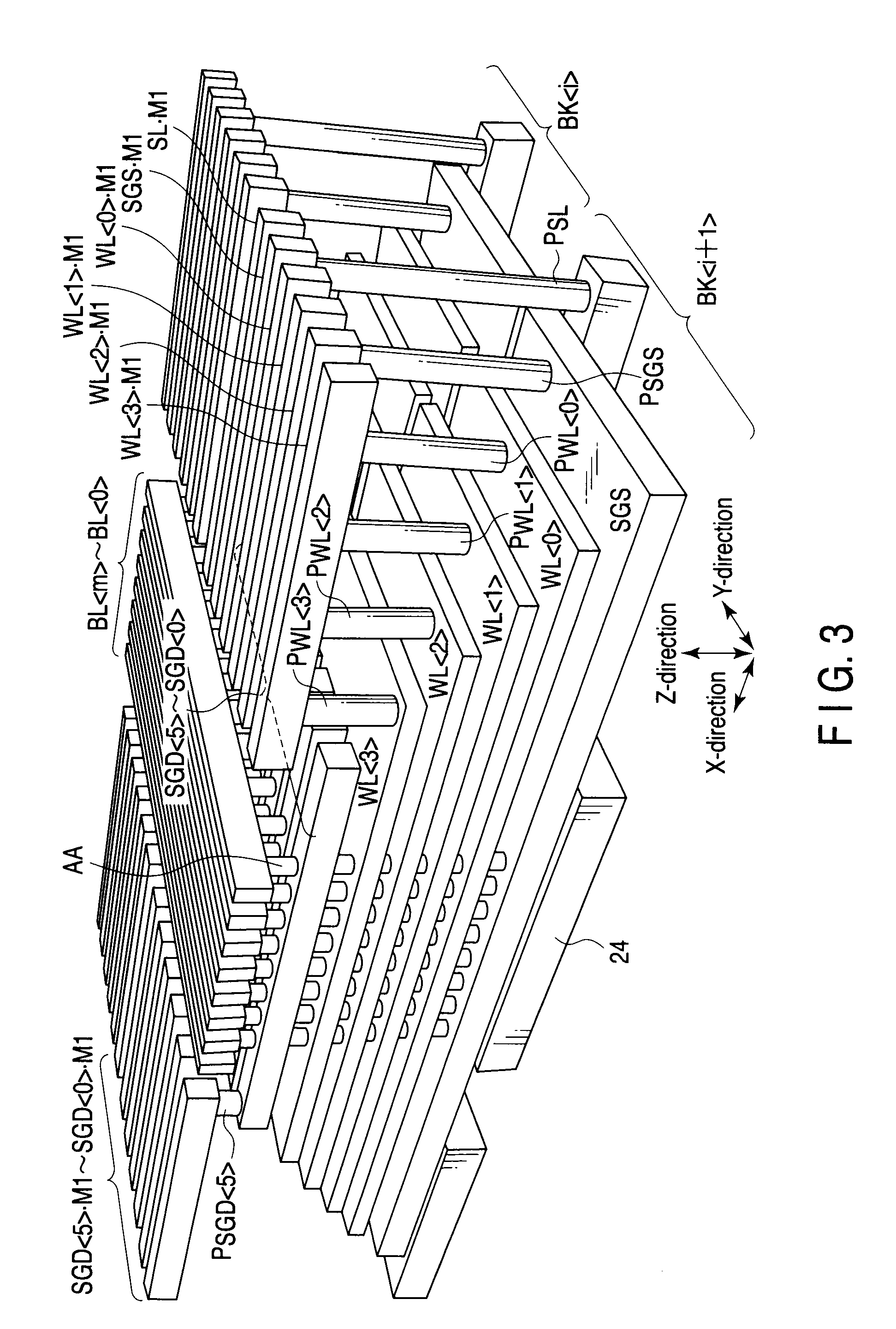
01 3D DRAM architecture and vertical stacking technology
Three-dimensional DRAM structures utilize vertical stacking of memory cells to increase storage density and reduce manufacturing costs per bit. This architecture enables higher capacity memory devices within smaller footprints by stacking multiple layers of memory cells vertically. The vertical integration approach reduces the chip area required compared to traditional planar designs, leading to improved cost effectiveness through better silicon utilization and increased yield per wafer.- 3D DRAM architecture and stacking technology: Three-dimensional DRAM structures utilize vertical stacking of memory cells to increase density and reduce cost per bit. This architecture involves stacking multiple layers of memory cells vertically, which allows for higher capacity in a smaller footprint. The technology addresses cost effectiveness by maximizing the number of memory cells per unit area while maintaining performance characteristics. Advanced fabrication techniques enable the creation of through-silicon vias and vertical interconnects that facilitate communication between stacked layers.
- BiCS FLASH memory cell structure and fabrication: Bit Cost Scalable FLASH memory employs a three-dimensional vertical NAND structure where memory cells are arranged in a vertical string configuration. This design significantly reduces the chip area required per bit, thereby improving cost effectiveness. The fabrication process involves forming vertical channels through multiple layers of alternating conductive and insulating materials, creating a compact memory array. This architecture enables continued scaling beyond the limitations of planar NAND technology while maintaining reliability and performance.
- Cost reduction through process integration: Manufacturing cost optimization is achieved through innovative process integration techniques that reduce the number of fabrication steps and improve yield. These methods include simplified lithography processes, shared manufacturing equipment between different memory types, and optimized material deposition techniques. The integration approach focuses on reducing mask counts, minimizing critical dimension requirements, and utilizing common processing steps across different memory technologies to lower overall production costs.
- Hybrid memory architecture for cost optimization: Combining different memory technologies in a single package or system provides cost-effective solutions by leveraging the advantages of each memory type. This approach integrates high-speed volatile memory with high-density non-volatile storage to optimize both performance and cost. The hybrid architecture allows for efficient data management where frequently accessed data resides in faster memory while bulk storage utilizes more cost-effective high-density memory. System-level optimization techniques balance performance requirements with manufacturing costs.
- Advanced packaging and interconnect solutions: Cost effectiveness is enhanced through innovative packaging technologies that enable higher integration density and improved electrical performance. These solutions include through-silicon via technology, wafer-level packaging, and advanced bonding techniques that reduce package size and interconnect lengths. The packaging approaches facilitate the integration of multiple memory dies in a compact form factor, reducing material costs and improving signal integrity. These technologies enable cost-effective scaling by allowing heterogeneous integration of different memory types and logic circuits.
02 BiCS FLASH memory cell structure and fabrication methods
Bit Cost Scalable FLASH memory technology employs vertical channel structures with multiple stacked word lines to achieve higher density storage. The fabrication process involves forming vertical holes through stacked gate layers and depositing channel materials, which reduces the number of lithography steps required. This manufacturing approach significantly lowers production costs while maintaining or improving performance characteristics, making it a cost-effective solution for high-capacity non-volatile memory applications.Expand Specific Solutions03 Cost reduction through shared peripheral circuits
Memory architectures that implement shared peripheral circuitry across multiple memory banks or layers reduce the overall die size and manufacturing complexity. By consolidating control circuits, sense amplifiers, and decoder structures, the total chip area dedicated to support circuitry is minimized. This design strategy improves cost effectiveness by maximizing the ratio of storage area to total chip area and reducing the number of required components.Expand Specific Solutions04 Advanced lithography and process integration techniques
Implementation of advanced manufacturing processes including multi-patterning lithography and self-aligned techniques enables finer feature sizes and tighter pitch scaling. These process innovations allow for increased memory density without requiring expensive next-generation lithography equipment. The integration of these techniques with existing fabrication infrastructure provides a cost-effective pathway to higher capacity memory devices while maintaining compatibility with established manufacturing processes.Expand Specific Solutions05 Hybrid memory architectures and system integration
Combining different memory technologies in hybrid configurations optimizes both performance and cost by leveraging the strengths of each technology. System-level integration approaches that stack different memory types or combine DRAM and FLASH in single packages reduce interconnect costs and improve overall system efficiency. These hybrid solutions provide cost-effective alternatives to single-technology approaches by balancing speed, capacity, and manufacturing expenses across the memory hierarchy.Expand Specific Solutions
Core Cost Engineering Innovations in 3D Memory
Three dimensional stacked nonvolatile semiconductor memory
PatentActiveUS20140355350A1
Innovation
- A novel layout is proposed where select gate lines on the bit line side are shared between two blocks, connected to a driver in a one-to-one relation, reducing the number of transistors required for driving these lines and thereby minimizing the area of the peripheral circuit.


Semiconductor device
PatentActiveUS20100090188A1
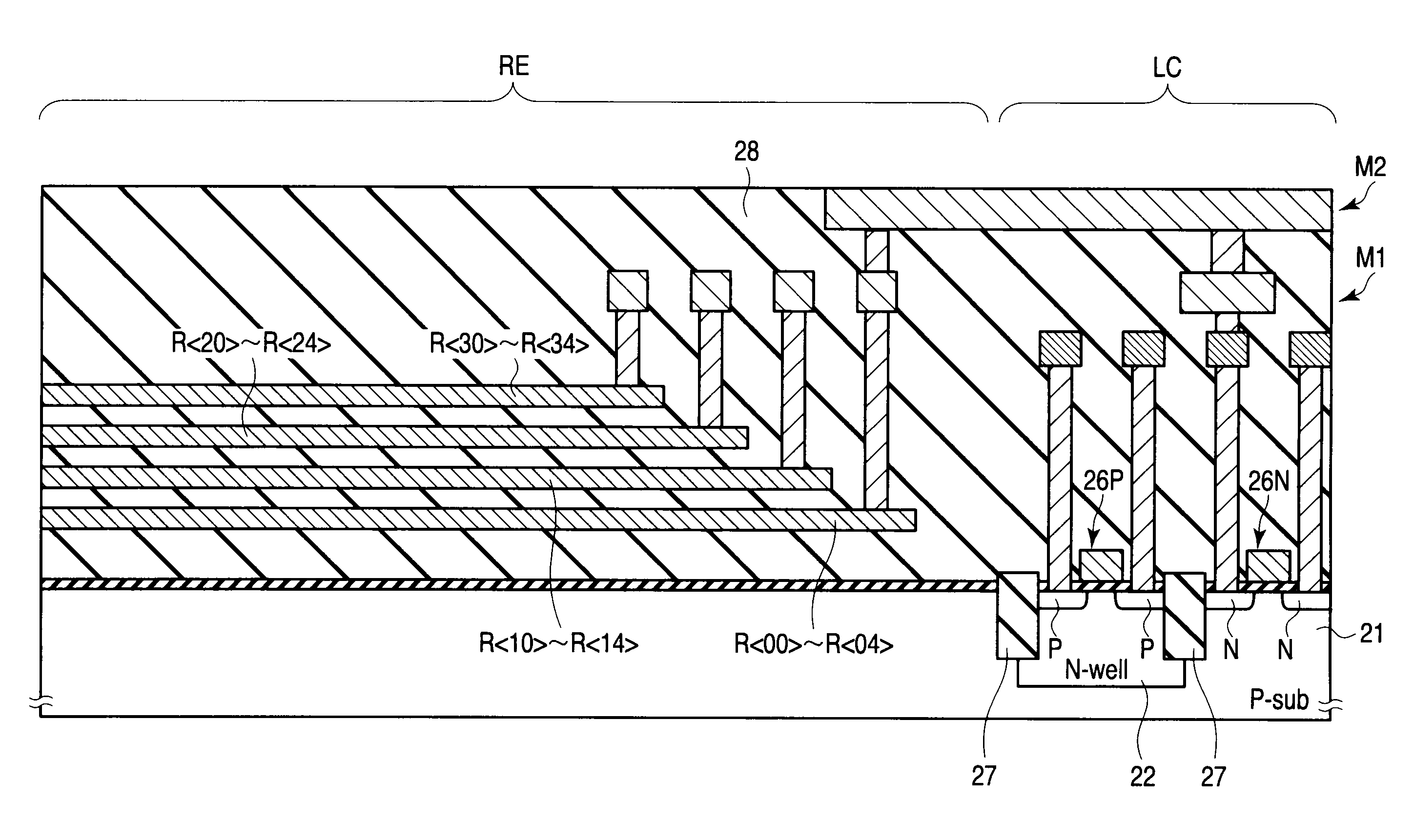
Innovation
- The conductive layers, made of polysilicon, are stacked with stairstep ends and connected in series by metal layers to form resistance and capacitance elements, allowing for 3-dimensional formation without additional processes, specifically odd-numbered layers forming one electrode and even-numbered layers forming another in capacitance elements.

Manufacturing Equipment Investment and ROI Analysis
The manufacturing equipment investment landscape for 3D DRAM and BiCS FLASH technologies presents distinctly different capital expenditure profiles and return trajectories. 3D DRAM fabrication requires sophisticated equipment including advanced lithography systems, specialized etching tools for vertical channel formation, and precision deposition equipment for wordline stacking. The initial capital investment typically ranges from $15-20 billion for a state-of-the-art fab, with equipment costs representing approximately 70-75% of total facility investment.
BiCS FLASH manufacturing demands equally complex but different equipment sets, focusing on high-aspect-ratio etching systems, charge trap layer deposition tools, and advanced metrology equipment for 3D structure verification. The capital intensity for BiCS FLASH fabs generally falls within $12-18 billion range, with equipment accounting for 65-70% of total investment. The lower relative cost stems from more mature process technologies and higher equipment utilization rates.
Equipment depreciation schedules significantly impact ROI calculations for both technologies. 3D DRAM equipment typically follows a 5-7 year depreciation cycle due to rapid technology evolution and performance requirements. Critical lithography tools may depreciate faster, often within 3-4 years, as new generations demand enhanced resolution capabilities. BiCS FLASH equipment generally maintains longer depreciation periods of 7-10 years, benefiting from more stable process requirements and extended technology node lifecycles.
Utilization rates directly influence ROI performance, with 3D DRAM fabs typically achieving 85-90% equipment utilization during peak demand periods. However, market volatility can reduce utilization to 60-70% during downturns, significantly impacting return calculations. BiCS FLASH manufacturing demonstrates more consistent utilization patterns, typically maintaining 80-85% rates due to steady enterprise and consumer storage demand.
The ROI timeline analysis reveals 3D DRAM investments typically achieve break-even within 3-4 years under favorable market conditions, with peak returns occurring in years 4-6. BiCS FLASH investments generally require 4-5 years for break-even but offer more predictable returns over 7-10 year periods. Equipment upgrade cycles further influence ROI, with 3D DRAM requiring more frequent technology refreshes, while BiCS FLASH benefits from evolutionary improvements that extend equipment productive life.
Supply Chain Risk Assessment for 3D Memory Production
The supply chain for 3D memory production presents distinct risk profiles for 3D DRAM and BiCS FLASH technologies, with implications extending beyond manufacturing costs to overall business continuity. Both technologies rely heavily on specialized materials and equipment sourced from a concentrated supplier base, creating vulnerability points that can significantly impact cost effectiveness calculations.
Material sourcing represents a critical risk factor, particularly for high-purity chemicals and rare earth elements essential in 3D memory fabrication. BiCS FLASH production requires specific tungsten compounds and specialized dielectric materials, while 3D DRAM manufacturing depends on capacitor materials including high-k dielectrics and metal electrodes. Supply disruptions for these materials can lead to production halts, with BiCS FLASH showing slightly higher resilience due to its simpler material stack compared to 3D DRAM's complex capacitor structures.
Equipment dependency poses another significant challenge, with both technologies requiring advanced lithography systems, atomic layer deposition tools, and specialized etching equipment. The limited number of suppliers for critical manufacturing equipment, particularly from ASML for EUV lithography and Applied Materials for deposition systems, creates bottlenecks that affect both memory types equally. However, 3D DRAM's more complex manufacturing process involving additional capacitor formation steps increases exposure to equipment-related supply chain disruptions.
Geopolitical factors substantially influence supply chain stability, with key manufacturing hubs concentrated in East Asia. Trade restrictions and export controls on semiconductor equipment and materials can disproportionately impact production costs and timelines. The recent semiconductor supply chain tensions have highlighted vulnerabilities in both 3D DRAM and BiCS FLASH production, though BiCS FLASH manufacturers have demonstrated greater supply chain diversification efforts.
Manufacturing complexity differences between the technologies create varying risk exposure levels. 3D DRAM's intricate capacitor structures require more specialized materials and tighter process controls, making it more susceptible to supply chain disruptions. BiCS FLASH's relatively simpler charge trap architecture provides more flexibility in material sourcing and alternative supplier adoption, contributing to improved supply chain resilience and potentially lower risk-adjusted costs.
Unlock deeper insights with PatSnap Eureka Quick Research — get a full tech report to explore trends and direct your research. Try now!
Generate Your Research Report Instantly with AI Agent
Supercharge your innovation with PatSnap Eureka AI Agent Platform!