

How to Optimize Clock Speed in 3D DRAM Structures
APR 15, 20269 MIN READ
Generate Your Research Report Instantly with AI Agent
PatSnap Eureka helps you evaluate technical feasibility & market potential.
3D DRAM Clock Speed Optimization Background and Goals
Three-dimensional DRAM technology represents a paradigm shift in memory architecture, emerging from the fundamental limitations of traditional planar memory designs. As semiconductor scaling approaches physical boundaries defined by atomic dimensions, the industry has pivoted toward vertical integration to maintain Moore's Law progression. This architectural evolution enables higher memory density while reducing the physical footprint, addressing the growing demands of data-intensive applications in artificial intelligence, high-performance computing, and mobile devices.
The transition from 2D to 3D DRAM structures introduces unprecedented complexity in signal timing and synchronization. Unlike conventional planar architectures where signal paths remain relatively uniform, 3D configurations create varying electrical characteristics across different vertical layers. These variations manifest as differential propagation delays, capacitive loading effects, and thermal gradients that directly impact clock distribution and timing closure. The challenge intensifies as manufacturers stack increasing numbers of memory layers to achieve competitive density targets.
Clock speed optimization in 3D DRAM structures has evolved through distinct technological phases. Early implementations focused on basic vertical stacking with minimal architectural modifications, achieving modest performance improvements while encountering significant timing challenges. Subsequent generations introduced sophisticated clock distribution networks, incorporating dedicated timing circuits and adaptive compensation mechanisms. Current state-of-the-art solutions employ advanced signal integrity techniques, including through-silicon vias with optimized impedance characteristics and multi-phase clocking schemes.
The primary technical objectives center on achieving uniform clock distribution across all memory layers while maintaining signal integrity and minimizing power consumption. This requires developing innovative solutions for managing inter-layer timing skew, which can exceed acceptable tolerances in deep 3D structures. Additionally, thermal management becomes critical as heat generation varies significantly between layers, creating temperature-dependent timing variations that must be compensated through dynamic adjustment mechanisms.
Contemporary optimization efforts target several key performance metrics including access latency reduction, bandwidth enhancement, and power efficiency improvement. The goal extends beyond simple frequency scaling to encompass comprehensive timing optimization that accounts for the unique characteristics of vertical memory architectures. Success in this domain directly translates to competitive advantages in memory-intensive applications where performance bottlenecks increasingly shift from computational units to memory subsystems.
Market Demand for High-Speed 3D Memory Solutions
The global memory market is experiencing unprecedented demand for high-speed solutions, driven by the exponential growth of data-intensive applications across multiple sectors. Cloud computing infrastructure, artificial intelligence workloads, and high-performance computing applications require memory systems capable of handling massive data throughput with minimal latency. This surge in computational requirements has created a substantial market opportunity for advanced 3D DRAM technologies that can deliver superior clock speeds and bandwidth performance.
Data centers represent the largest segment driving demand for high-speed 3D memory solutions. Modern server architectures supporting virtualization, containerization, and distributed computing frameworks require memory subsystems that can sustain continuous high-bandwidth operations. The proliferation of machine learning training clusters and inference engines has further intensified the need for memory technologies that can eliminate bottlenecks in data processing pipelines.
Consumer electronics markets are simultaneously pushing memory performance boundaries through gaming applications, mobile devices, and emerging augmented reality platforms. Graphics processing units and specialized AI accelerators integrated into consumer products demand memory solutions with optimized clock speeds to support real-time rendering, complex computational tasks, and seamless user experiences across multiple concurrent applications.
The automotive industry presents an emerging high-growth segment for advanced memory technologies. Autonomous driving systems, advanced driver assistance features, and in-vehicle infotainment platforms require memory solutions capable of processing sensor data streams in real-time while maintaining reliability under harsh operating conditions. These applications demand both high-speed performance and enhanced durability characteristics.
Enterprise applications including financial trading systems, scientific simulation platforms, and real-time analytics engines represent specialized market segments with stringent performance requirements. These applications often require memory systems with consistent low-latency access patterns and sustained high-bandwidth capabilities to support mission-critical operations.
The telecommunications sector, particularly with the deployment of 5G networks and edge computing infrastructure, creates additional demand for high-performance memory solutions. Network function virtualization and software-defined networking implementations require memory subsystems that can handle dynamic workload scaling while maintaining predictable performance characteristics across diverse operational scenarios.
Current State and Challenges of 3D DRAM Clock Performance
The current landscape of 3D DRAM technology presents a complex interplay between architectural innovation and performance limitations, particularly in clock speed optimization. Modern 3D DRAM structures have evolved from traditional planar designs to sophisticated vertical architectures, enabling higher density storage while introducing new timing challenges. Leading manufacturers have achieved commercial implementations with stack heights exceeding 100 layers, yet clock speeds remain constrained by fundamental physical and electrical limitations inherent to three-dimensional structures.
Contemporary 3D DRAM implementations face significant signal integrity challenges that directly impact clock performance. The vertical interconnect structures, including through-silicon vias and word line staircases, introduce parasitic capacitances and resistances that degrade signal quality and limit maximum operating frequencies. Current production devices typically operate at clock speeds 20-30% lower than their 2D counterparts due to these architectural constraints.
Power delivery represents another critical bottleneck in current 3D DRAM designs. The increased current density requirements in vertically stacked structures create voltage drop issues and thermal hotspots that force conservative clock speed settings. Existing power distribution networks struggle to maintain stable voltage levels across all memory layers simultaneously, particularly during high-frequency switching operations.
Thermal management emerges as a fundamental challenge limiting clock speed scalability in 3D DRAM structures. Heat dissipation becomes increasingly difficult as layer count increases, with internal layers experiencing significantly higher temperatures than peripheral ones. This thermal gradient creates timing skew across different stack levels and necessitates reduced operating frequencies to ensure reliability and data integrity.
Manufacturing variability poses additional constraints on clock speed optimization in current 3D DRAM technologies. Process variations in vertical etching, layer deposition, and contact formation result in non-uniform electrical characteristics across the memory array. These variations manifest as timing uncertainties that require substantial guard bands, effectively reducing achievable clock speeds below theoretical limits.
Current industry solutions primarily focus on architectural modifications and process improvements to address these challenges. Advanced error correction schemes, adaptive timing controls, and improved thermal interface materials represent the state-of-the-art approaches, yet significant performance gaps remain compared to theoretical potential.
Existing Clock Speed Enhancement Solutions for 3D DRAM
01 3D DRAM architecture with vertical cell structures
Three-dimensional DRAM structures utilize vertical stacking of memory cells to increase density and reduce signal path lengths. This architecture enables faster access times and improved clock speeds by minimizing the distance signals must travel between cells. The vertical arrangement allows for more efficient use of chip area while maintaining or improving performance characteristics compared to traditional planar designs.- 3D DRAM architecture with vertical cell structures: Three-dimensional DRAM structures utilize vertical stacking of memory cells to increase density and reduce signal path lengths. This architecture enables faster access times and improved clock speed performance by minimizing the distance signals must travel between cells. The vertical arrangement allows for more efficient use of chip area while maintaining or improving operational frequencies.
- Clock signal distribution networks for 3D memory: Advanced clock distribution systems are designed specifically for three-dimensional memory architectures to ensure synchronized timing across multiple layers. These networks employ specialized routing techniques and buffering schemes to maintain signal integrity and minimize skew between different vertical levels. The distribution architecture is critical for achieving high-speed operation in stacked memory configurations.
- Timing control circuits for high-speed 3D DRAM operation: Specialized timing control circuits manage the synchronization of read and write operations in three-dimensional memory structures operating at elevated clock frequencies. These circuits incorporate delay compensation mechanisms and adaptive timing adjustments to account for variations in signal propagation through vertical interconnects. The control systems enable reliable operation at higher clock speeds while maintaining data integrity.
- Through-silicon via (TSV) technology for clock signal transmission: Through-silicon vias provide vertical electrical connections between stacked memory layers, serving as pathways for clock signal distribution in three-dimensional DRAM structures. The design and placement of these vias are optimized to minimize parasitic capacitance and inductance, which directly impacts the maximum achievable clock frequency. Proper TSV implementation is essential for maintaining signal quality and enabling high-speed operation.
- Power delivery and thermal management for high-frequency 3D DRAM: Efficient power distribution networks and thermal management solutions are implemented to support high clock speed operation in three-dimensional memory structures. These systems address the increased power density and heat generation associated with stacked architectures operating at elevated frequencies. Proper thermal and power management enables sustained high-speed performance while preventing reliability issues.
02 Clock signal distribution networks for 3D memory
Specialized clock distribution networks are designed to deliver synchronized timing signals across multiple layers of three-dimensional memory structures. These networks address the challenges of signal skew and propagation delays inherent in vertically stacked architectures. Advanced distribution schemes ensure uniform clock delivery to all memory cells regardless of their position in the 3D structure, enabling consistent high-speed operation.Expand Specific Solutions03 High-speed interface circuits for 3D DRAM
Interface circuits are optimized to support high-frequency operation in three-dimensional memory architectures. These circuits include sense amplifiers, input/output buffers, and timing control logic specifically designed to handle the increased complexity of 3D structures. The interface designs compensate for parasitic capacitances and inductances associated with vertical interconnects to maintain signal integrity at elevated clock frequencies.Expand Specific Solutions04 Through-silicon via technology for vertical interconnection
Through-silicon vias provide electrical connections between stacked memory layers in three-dimensional DRAM structures. These vertical interconnects are critical for achieving high-speed data transfer and clock signal distribution across multiple die layers. The technology enables reduced interconnect lengths and lower parasitic effects, contributing to improved operating frequencies and reduced power consumption.Expand Specific Solutions05 Timing control and synchronization methods
Advanced timing control schemes manage the complex synchronization requirements of three-dimensional memory arrays operating at high clock speeds. These methods include adaptive delay compensation, phase-locked loop circuits, and delay-locked loop implementations tailored for 3D architectures. The timing control systems account for variations in signal propagation across different layers and ensure reliable operation across the entire memory structure at maximum clock frequencies.Expand Specific Solutions
Key Players in 3D DRAM and Memory Controller Industry
The 3D DRAM clock speed optimization market represents a rapidly evolving segment within the advanced memory semiconductor industry, currently in its growth phase with significant technological and commercial potential. The market is experiencing substantial expansion driven by increasing demand for high-performance computing, AI applications, and data-intensive workloads requiring faster memory access speeds. From a technology maturity perspective, the field demonstrates varying levels of development across key players. Industry leaders like Samsung Electronics, SK Hynix, and Intel possess mature 3D DRAM technologies with established optimization capabilities, while emerging players such as ChangXin Memory Technologies and Yangtze Memory Technologies are rapidly advancing their technical competencies. Research institutions including Imec and Katholieke Universiteit Leuven contribute fundamental innovations, while companies like NVIDIA and MediaTek drive application-specific optimization requirements. The competitive landscape shows a mix of established memory manufacturers with proven track records and newer entrants leveraging innovative approaches to challenge traditional architectures.
Samsung Electronics Co., Ltd.
Technical Solution: Samsung has developed advanced 3D DRAM architectures with optimized clock speed management through their proprietary Through-Silicon Via (TSV) technology and adaptive voltage scaling mechanisms. Their approach includes implementing dynamic frequency scaling algorithms that adjust clock speeds based on thermal conditions and workload demands in vertically stacked memory cells. The company utilizes advanced process nodes and employs sophisticated power delivery networks with dedicated clock distribution trees to minimize skew and jitter across multiple DRAM layers. Samsung's 3D DRAM solutions incorporate intelligent thermal management systems that monitor temperature gradients and automatically adjust operating frequencies to maintain optimal performance while preventing thermal throttling in dense memory configurations.
Strengths: Market leadership in memory technology, extensive R&D resources, proven manufacturing capabilities. Weaknesses: High development costs, complex thermal management challenges in dense 3D structures.
Intel Corp.
Technical Solution: Intel approaches 3D DRAM clock speed optimization through their integrated memory controller designs and advanced packaging technologies. Their solution combines on-die memory controllers with sophisticated clock distribution networks that utilize adaptive timing mechanisms to compensate for process variations and thermal effects in 3D structures. Intel employs machine learning algorithms to predict optimal clock frequencies based on workload characteristics and system conditions. The company's approach includes implementing advanced signal integrity techniques such as equalization and pre-emphasis to maintain high-speed operation across multiple memory layers. Intel also develops custom memory interfaces that can dynamically adjust timing parameters and clock speeds to maximize bandwidth while ensuring data integrity in complex 3D DRAM configurations.
Strengths: Strong processor-memory integration expertise, advanced packaging technologies, comprehensive system-level optimization. Weaknesses: Limited pure memory manufacturing capabilities, focus primarily on processor-centric solutions.
Core Innovations in 3D DRAM Timing and Signal Integrity
Method and apparatus for tuning phase of clock signal
PatentActiveUS8242819B2
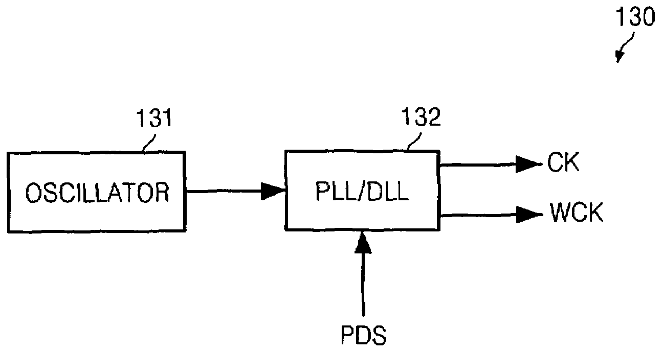
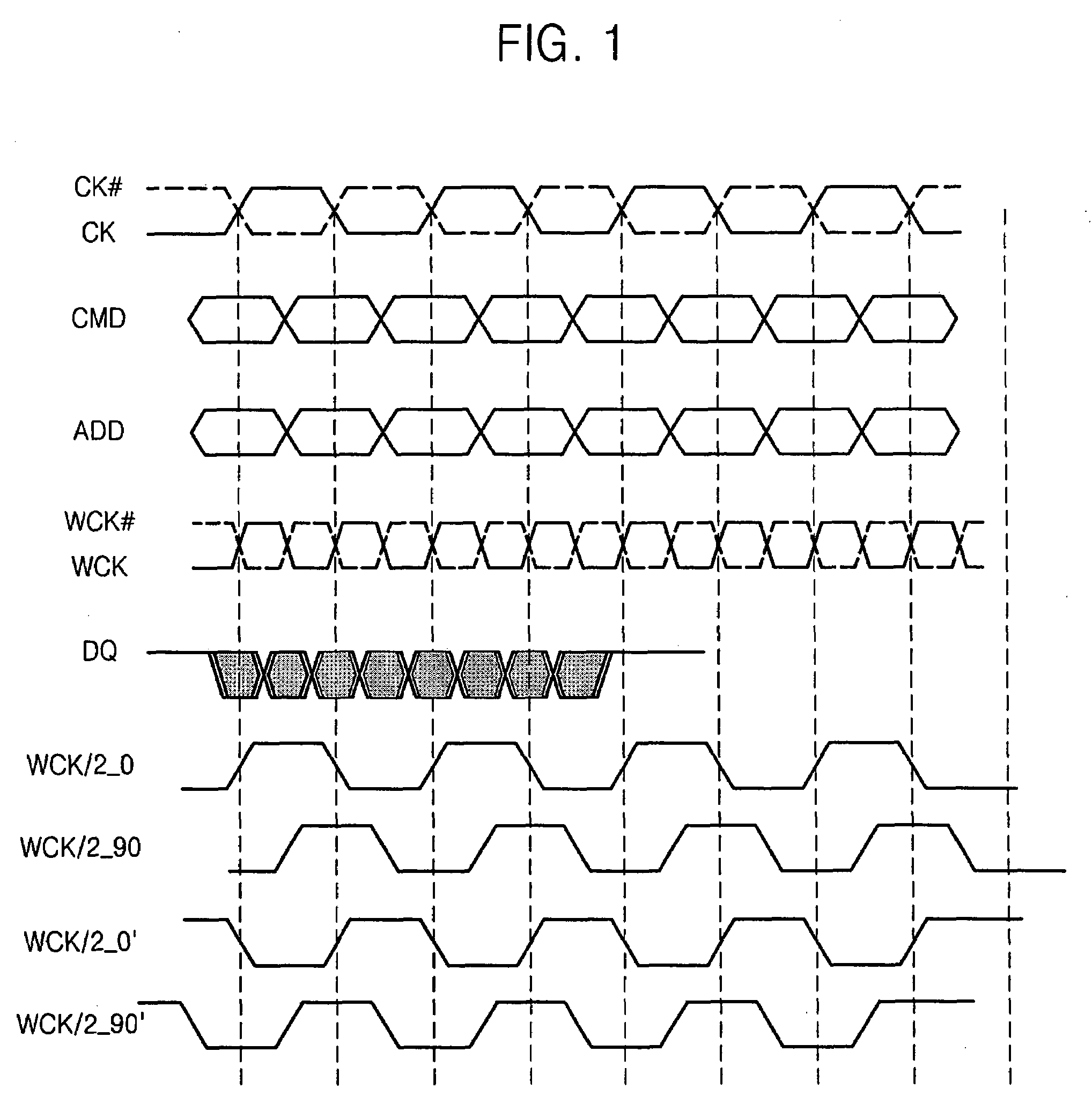
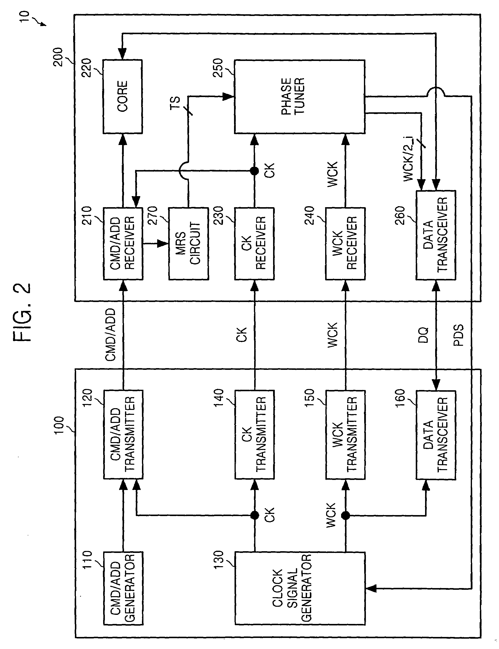
Innovation
- A semiconductor apparatus and method that tunes the phase of a data clock signal with a different frequency than the main clock signal by generating frequency-divided clock signals and comparing their phases to synchronize with the main clock signal, allowing for faster data transmission and reception.


Method and apparatus for tuning phase of clock signal
PatentActiveUS20090251181A1
Innovation
- A semiconductor memory apparatus is designed with a phase tuner that receives a data clock signal with a different frequency, generates frequency-divided clock signals, and compares their phases with the main clock signal to adjust and synchronize them, allowing for the generation of multiphase frequency-divided clock signals to optimize data transmission speed.

Thermal Management Impact on 3D DRAM Clock Performance
Thermal management represents one of the most critical bottlenecks limiting clock speed optimization in 3D DRAM structures. As memory cells are stacked vertically in multiple layers, heat generation becomes concentrated within a smaller footprint, creating significant thermal gradients that directly impact electrical performance and timing characteristics.
The fundamental challenge stems from the exponential relationship between temperature and leakage current in semiconductor devices. In 3D DRAM architectures, elevated temperatures cause increased junction leakage, which degrades signal integrity and forces longer refresh cycles. This thermal-induced performance degradation becomes particularly pronounced at higher clock frequencies, where switching losses generate additional heat, creating a self-limiting feedback loop that constrains maximum achievable speeds.
Heat dissipation in vertically stacked memory presents unique challenges compared to planar designs. Traditional heat removal relies primarily on substrate conduction, but in 3D structures, the central layers experience poor thermal coupling to heat sinks. This results in non-uniform temperature distributions across the stack, with inner layers operating at significantly higher temperatures than peripheral ones. Such thermal gradients create timing skew between different memory banks, complicating clock distribution and synchronization.
Advanced thermal management techniques are emerging as enablers for higher clock speeds in 3D DRAM. Through-silicon vias (TSVs) are being engineered not only for electrical connectivity but also as thermal conduits, utilizing high-conductivity materials like copper to create vertical heat paths. Micro-channel cooling integrated within the die stack shows promise for active heat removal, though implementation complexity remains challenging.
Temperature-aware clock management strategies are becoming essential for optimizing performance while maintaining reliability. Dynamic thermal monitoring enables real-time clock frequency scaling based on thermal conditions, allowing systems to operate at maximum safe speeds. Predictive thermal modeling helps anticipate hot spots and proactively adjust operating parameters before thermal limits are reached.
The interplay between thermal management and clock optimization requires holistic design approaches that consider power delivery, signal integrity, and heat removal as interconnected challenges rather than isolated problems.
Power Efficiency Considerations in High-Speed 3D Memory
Power efficiency emerges as a critical design constraint when pursuing high-speed operation in 3D DRAM structures. The vertical stacking architecture inherently creates thermal challenges that directly impact power consumption patterns, as heat dissipation becomes increasingly complex with multiple memory layers. Traditional power management strategies require fundamental reconsideration to address the unique thermal and electrical characteristics of three-dimensional memory configurations.
The relationship between clock speed optimization and power consumption in 3D DRAM follows non-linear scaling patterns. As operating frequencies increase, dynamic power consumption rises quadratically with voltage scaling, while leakage power becomes more pronounced due to elevated junction temperatures in stacked structures. This thermal coupling effect between adjacent memory layers creates localized hotspots that can degrade performance and reliability, necessitating sophisticated power management techniques.
Advanced power gating strategies prove essential for maintaining efficiency in high-speed 3D memory systems. Selective activation of memory banks and layers allows for dynamic power scaling based on access patterns, reducing unnecessary power consumption in idle regions. Fine-grained power domain partitioning enables independent voltage and frequency scaling across different memory layers, optimizing the trade-off between performance and energy consumption.
Voltage scaling techniques specifically tailored for 3D architectures offer significant efficiency improvements. Adaptive voltage scaling algorithms can dynamically adjust supply voltages based on workload characteristics and thermal conditions, maintaining optimal performance while minimizing power overhead. Near-threshold voltage operation in less frequently accessed memory layers provides substantial energy savings without compromising overall system performance.
Clock distribution network optimization plays a crucial role in power efficiency considerations. Implementing hierarchical clock gating structures and localized clock generation reduces power consumption associated with global clock distribution across multiple memory layers. Advanced clock management techniques, including dynamic frequency scaling and clock pause mechanisms, enable fine-tuned power control based on real-time access patterns and thermal feedback.
Emerging power delivery architectures, such as distributed voltage regulation and on-chip power management units, provide enhanced efficiency for high-speed 3D memory operations. These solutions enable precise power control at the layer level, supporting aggressive power scaling strategies while maintaining signal integrity and timing requirements across the three-dimensional memory structure.
Unlock deeper insights with PatSnap Eureka Quick Research — get a full tech report to explore trends and direct your research. Try now!
Generate Your Research Report Instantly with AI Agent
Supercharge your innovation with PatSnap Eureka AI Agent Platform!