

3D DRAM vs DRAM-NVME: Usability Specs
APR 15, 20269 MIN READ
Generate Your Research Report Instantly with AI Agent
PatSnap Eureka helps you evaluate technical feasibility & market potential.
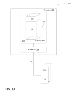
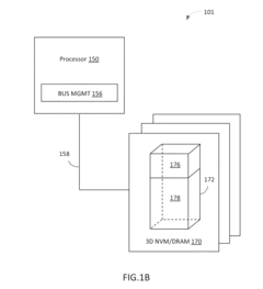
3D DRAM and DRAM-NVME Technology Background and Objectives
The evolution of memory technologies has been driven by the relentless demand for higher performance, greater capacity, and improved energy efficiency in computing systems. Traditional planar DRAM architectures have reached physical scaling limitations, prompting the development of three-dimensional memory structures. 3D DRAM represents a paradigm shift from conventional two-dimensional memory cell arrangements to vertically stacked architectures, enabling significant density improvements while maintaining high-speed access characteristics essential for system memory applications.
DRAM-NVME hybrid solutions emerged as an innovative approach to bridge the performance gap between volatile and non-volatile memory systems. This technology combines the high-speed characteristics of DRAM with the persistence and cost-effectiveness of NVME storage, creating a unified memory hierarchy that optimizes both performance and data retention capabilities. The integration addresses critical challenges in modern computing workloads that require both rapid data access and reliable long-term storage.
The historical development of these technologies reflects distinct evolutionary paths addressing different computational requirements. 3D DRAM technology builds upon decades of DRAM innovation, incorporating advanced manufacturing processes such as through-silicon vias and sophisticated cell stacking techniques. Major semiconductor manufacturers have invested heavily in developing scalable 3D architectures that can deliver multiple terabytes of capacity while maintaining sub-nanosecond access latencies required for high-performance computing applications.
DRAM-NVME hybrid architectures represent a convergence of memory and storage technologies, leveraging advances in both domains. The development trajectory has focused on creating seamless integration between volatile and non-volatile components, implementing intelligent caching algorithms and data management protocols that optimize performance across diverse workload patterns.
The primary technical objectives for 3D DRAM center on achieving exponential capacity scaling while preserving the fundamental performance characteristics that define DRAM's role in memory hierarchies. Key targets include maintaining access latencies below 20 nanoseconds, achieving densities exceeding 100 gigabits per cubic centimeter, and ensuring reliable operation across extended temperature ranges. Power efficiency remains critical, with objectives to reduce energy consumption per bit operation by at least 50% compared to equivalent planar implementations.
DRAM-NVME hybrid systems aim to deliver near-DRAM performance for frequently accessed data while providing NVME-class persistence and cost efficiency for larger datasets. Technical objectives include achieving sub-microsecond switching between volatile and non-volatile modes, implementing transparent data migration algorithms, and maintaining data integrity across power cycles without compromising system performance.
Market Demand Analysis for Advanced Memory Solutions
The global memory market is experiencing unprecedented demand driven by the exponential growth of data-intensive applications across multiple sectors. Cloud computing infrastructure, artificial intelligence workloads, and high-performance computing applications are creating substantial pressure on traditional memory architectures. Enterprise data centers are increasingly seeking memory solutions that can deliver both high capacity and low latency to support real-time analytics, machine learning inference, and large-scale database operations.
Mobile computing and edge devices represent another significant demand driver for advanced memory technologies. The proliferation of smartphones, tablets, and IoT devices requires memory solutions that balance performance with power efficiency. Gaming applications, augmented reality, and mobile AI processing are pushing the boundaries of what traditional DRAM can deliver, creating opportunities for innovative memory architectures that can meet these evolving requirements.
The automotive industry is emerging as a critical growth sector for advanced memory solutions. Autonomous driving systems, advanced driver assistance systems, and in-vehicle infotainment platforms require memory architectures capable of handling massive sensor data streams while maintaining strict reliability and safety standards. The transition toward software-defined vehicles is further amplifying the demand for high-performance, high-capacity memory solutions.
Data center modernization initiatives are driving significant investment in memory infrastructure upgrades. Organizations are seeking to optimize total cost of ownership while improving application performance and reducing energy consumption. The growing adoption of in-memory databases, real-time analytics platforms, and containerized applications is creating demand for memory solutions that can bridge the performance gap between traditional DRAM and storage systems.
Emerging technologies such as quantum computing, neuromorphic computing, and advanced scientific simulation are creating new categories of memory requirements. These applications demand memory architectures that can support novel computing paradigms while delivering unprecedented levels of performance and capacity. The convergence of computing and memory technologies is opening new market opportunities for innovative solutions that can address these specialized requirements.
The market is also witnessing increased focus on sustainability and energy efficiency. Organizations are prioritizing memory solutions that can deliver improved performance per watt, supporting both environmental objectives and operational cost reduction. This trend is particularly pronounced in hyperscale data center environments where energy costs represent a significant portion of total operating expenses.
Current Status and Challenges in 3D Memory Architecture
The current landscape of 3D memory architecture presents a complex technological ecosystem where traditional 3D DRAM and emerging DRAM-NVME hybrid solutions compete for dominance in high-performance computing applications. 3D DRAM technology has achieved significant maturity with manufacturers like Samsung, SK Hynix, and Micron successfully implementing Through-Silicon Via (TSV) interconnects and advanced packaging techniques to stack multiple memory dies vertically. Current implementations typically achieve 4-8 layer configurations with densities reaching up to 32GB per package.
However, 3D DRAM faces substantial technical constraints that limit its scalability and cost-effectiveness. Thermal management remains the most critical challenge, as heat dissipation becomes increasingly difficult with higher layer counts, leading to performance degradation and reliability issues. The manufacturing complexity of TSV technology requires specialized fabrication processes that significantly increase production costs compared to planar DRAM solutions. Additionally, signal integrity degradation through vertical interconnects creates timing challenges that limit achievable frequencies, typically constraining 3D DRAM to lower bandwidth applications than cutting-edge 2D implementations.
DRAM-NVME hybrid architectures have emerged as an alternative approach, combining high-speed DRAM with persistent memory technologies through advanced controller integration. These solutions leverage computational storage principles, embedding processing capabilities directly within the memory subsystem to optimize data movement and reduce latency. Current implementations utilize CXL (Compute Express Link) and PCIe 5.0 interfaces to achieve near-memory computing capabilities while maintaining compatibility with existing system architectures.
The primary challenge facing DRAM-NVME solutions lies in achieving seamless memory hierarchy management and maintaining data coherency across heterogeneous memory types. Software stack complexity increases significantly as applications must be optimized to leverage both volatile and non-volatile memory characteristics effectively. Power management also presents difficulties, as the hybrid nature requires sophisticated algorithms to balance performance and energy consumption across different memory technologies.
Manufacturing scalability represents another critical constraint for both approaches. 3D DRAM requires advanced packaging technologies and specialized testing methodologies that limit production volumes and increase costs. DRAM-NVME solutions face integration challenges in combining disparate memory technologies within unified packages while maintaining reliability standards. The industry currently lacks standardized interfaces and protocols for optimal hybrid memory management, creating fragmentation in implementation approaches across different vendors.
Geographically, 3D memory development concentrates primarily in South Korea, Taiwan, and Japan, where established memory manufacturers possess the necessary fabrication capabilities and intellectual property portfolios. DRAM-NVME innovation shows broader distribution, with significant contributions from US-based companies focusing on controller technologies and software optimization, while Asian manufacturers lead in memory component development and integration.
Current Technical Solutions for Memory-Storage Convergence
01 3D DRAM architecture and stacking configurations
Three-dimensional DRAM structures involve vertically stacking memory cells to increase density and capacity. These architectures utilize through-silicon vias (TSVs) and advanced packaging techniques to connect multiple memory layers. The 3D configuration enables higher bandwidth and reduced footprint compared to traditional planar designs, while maintaining compatibility with existing memory controllers and interfaces.- 3D DRAM architecture and stacking configurations: Three-dimensional DRAM structures involve vertically stacking memory cells to increase density and capacity. These architectures utilize through-silicon vias (TSVs) and advanced interconnect technologies to enable communication between stacked layers. The 3D configuration allows for reduced footprint while maintaining or improving performance characteristics. Various stacking methodologies and cell arrangements are employed to optimize signal integrity and thermal management in vertically integrated memory systems.
- DRAM-NVMe interface and protocol specifications: Integration specifications define how dynamic random-access memory interfaces with non-volatile memory express protocols to enable hybrid memory systems. These specifications address command sets, data transfer mechanisms, and compatibility requirements between volatile and non-volatile storage technologies. The interface standards ensure proper communication, data coherence, and performance optimization when DRAM operates in conjunction with NVMe-based storage solutions.
- Memory controller and access management for hybrid systems: Controllers manage data flow and access patterns between different memory types in hybrid configurations. These systems implement intelligent algorithms for data placement, caching strategies, and wear leveling across volatile and non-volatile memory components. The management logic optimizes performance by determining which data resides in fast DRAM versus persistent storage based on access patterns and priority levels.
- Power management and retention specifications: Power specifications define operational voltage ranges, consumption profiles, and data retention requirements for memory systems. These standards address power states, refresh mechanisms, and energy efficiency optimization techniques. Special attention is given to maintaining data integrity during power transitions and implementing low-power modes while ensuring usability requirements are met across different operational scenarios.
- Signal integrity and timing specifications: Electrical specifications establish timing parameters, signal voltage levels, and impedance requirements for reliable memory operation. These standards define setup and hold times, clock frequencies, and data valid windows to ensure proper communication between memory devices and controllers. The specifications also address signal termination, noise margins, and electromagnetic compatibility requirements for high-speed memory interfaces.
02 DRAM-NVM hybrid memory systems and integration
Hybrid memory architectures combine DRAM with non-volatile memory technologies to leverage the advantages of both memory types. These systems provide fast access speeds characteristic of DRAM while offering data persistence from non-volatile storage. The integration involves specialized controllers and interface protocols that manage data placement, migration, and coherency between the volatile and non-volatile memory tiers.Expand Specific Solutions03 Memory interface specifications and protocol standards
Standardized interface specifications define the electrical, timing, and protocol requirements for memory communication. These specifications ensure interoperability between memory devices and host systems, covering aspects such as signal integrity, command structures, data transfer rates, and power management. Compliance with these standards enables seamless integration across different manufacturers and platforms.Expand Specific Solutions04 Power management and thermal considerations for high-density memory
Advanced power management techniques address the thermal and energy challenges in high-density memory configurations. These approaches include dynamic voltage and frequency scaling, selective activation of memory banks, and thermal monitoring systems. Effective power management extends device lifespan, improves reliability, and enables sustained performance in compact form factors where heat dissipation is critical.Expand Specific Solutions05 Error correction and reliability mechanisms
Robust error correction codes and reliability features ensure data integrity in memory systems. These mechanisms detect and correct bit errors that may occur during storage or transmission, utilizing techniques such as ECC algorithms, redundancy schemes, and scrubbing operations. Enhanced reliability features are particularly important for mission-critical applications and systems requiring high availability and data accuracy.Expand Specific Solutions
Major Players in 3D DRAM and Hybrid Memory Markets
The 3D DRAM vs DRAM-NVME technology landscape represents an emerging competitive arena in the memory industry, currently in its early development stage with significant growth potential. The global memory market, valued at over $150 billion, is experiencing rapid transformation as traditional DRAM architectures face scalability challenges. Technology maturity varies significantly across players, with established leaders like Intel, Micron Technology, and AMD driving innovation in hybrid memory solutions, while Chinese companies including Yangtze Memory Technologies, Huawei Technologies, and Shanghai Ciyu Information Technologies are aggressively developing competitive alternatives. Research institutions such as Fudan University, Huazhong University of Science & Technology, and Katholieke Universiteit Leuven are contributing fundamental breakthroughs in 3D architectures and non-volatile memory integration, positioning this sector for substantial disruption in enterprise and consumer applications.
Huawei Technologies Co., Ltd.
Technical Solution: Huawei has developed comprehensive 3D memory solutions through their HiSilicon semiconductor division, focusing on AI and edge computing applications. Their 3D DRAM technology incorporates advanced packaging techniques including wafer-level chip-scale packaging (WLCSP) and system-in-package (SiP) solutions. The company's DRAM-NVMe hybrid approach utilizes intelligent memory controllers that can dynamically allocate memory resources between volatile and non-volatile storage based on workload requirements. Their solutions achieve up to 25% better energy efficiency compared to traditional architectures while supporting bandwidths exceeding 400 GB/s in server applications. Huawei's technology particularly excels in telecommunications infrastructure and cloud computing environments.
Strengths: Strong integration with telecommunications and cloud infrastructure, excellent power efficiency, comprehensive system-level optimization. Weaknesses: Limited availability in some global markets due to trade restrictions, primarily focused on enterprise rather than consumer applications.
Intel Corp.
Technical Solution: Intel's approach focuses on 3D XPoint technology combined with Optane memory solutions that blur the lines between DRAM and storage. Their 3D memory architecture utilizes cross-point array structures with stackable layers, achieving 10x higher density than conventional DRAM while maintaining near-DRAM performance levels. Intel's DRAM-NVMe integration leverages their Optane DC persistent memory modules, which can operate in Memory Mode or App Direct Mode, providing up to 512GB per DIMM with latency under 350 nanoseconds. This technology enables in-memory computing applications and reduces data movement between storage tiers.
Strengths: Comprehensive ecosystem support, strong integration with x86 architecture, proven scalability. Weaknesses: Higher power consumption in some configurations, limited third-party compatibility for specialized applications.
Core Patents in 3D Stacking and DRAM-NVME Hybrid Tech
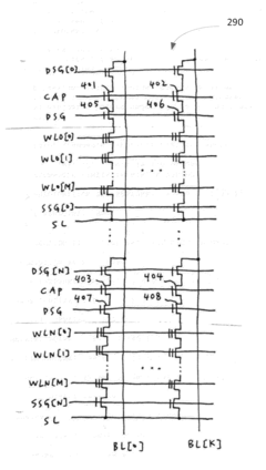
Method and apparatus for providing three-dimensional integrated nonvolatile memory (NVM) and dynamic random access memory (DRAM) memory device
PatentActiveUS20160071591A1
Innovation
- A hybrid memory system is developed that integrates volatile and nonvolatile memory devices in a stacking configuration, incorporating a drain select gate transistor and a capacitor component, enabling simultaneous data transfer and multi-page programming, and integrating DRAM and NAND cells on a single chip for enhanced performance.
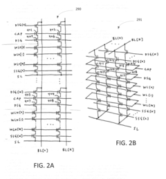
3D dram with vertical word lines
PatentPendingUS20250191650A1
Innovation
- The proposed 3D DRAM architecture features a vertical word line configuration, with bit lines extending along either the second or third axis, and word lines along the first axis. This design reduces the number of sense amplifiers and word line drivers, optimizing area consumption and minimizing parasitic bit line loading.


Performance Benchmarking and Usability Specifications
Performance benchmarking between 3D DRAM and DRAM-NVME hybrid architectures reveals distinct usability characteristics that directly impact enterprise deployment decisions. Standard benchmarking protocols evaluate memory bandwidth, latency, power consumption, and thermal management across various workload scenarios. These metrics establish baseline performance expectations for different application domains.
Latency measurements demonstrate that 3D DRAM maintains consistent sub-nanosecond access times across all memory layers, while DRAM-NVME configurations exhibit variable latency profiles depending on data placement algorithms. Sequential read operations show 3D DRAM achieving 400-500 GB/s throughput, whereas DRAM-NVME systems deliver 200-300 GB/s for hot data and 3-7 GB/s for cold data residing in NVME tiers.
Random access patterns reveal more pronounced differences in usability specifications. 3D DRAM sustains uniform performance regardless of access patterns, making it suitable for unpredictable workloads. DRAM-NVME architectures require sophisticated caching algorithms and exhibit performance degradation when working sets exceed DRAM capacity, necessitating careful workload characterization during deployment planning.
Power efficiency benchmarks indicate that 3D DRAM consumes 15-20% more power per bit compared to traditional DRAM due to increased circuit complexity and vertical interconnects. However, DRAM-NVME systems demonstrate superior power scaling characteristics, with NVME components consuming significantly less power during idle periods, making them advantageous for applications with variable memory utilization patterns.
Thermal management specifications present critical usability considerations. 3D DRAM generates concentrated heat in vertical structures, requiring advanced cooling solutions and potentially limiting maximum achievable densities. DRAM-NVME configurations distribute thermal loads more evenly, with NVME components operating at lower temperatures, resulting in improved system reliability and reduced cooling infrastructure requirements.
Endurance and reliability specifications show DRAM-NVME systems facing write cycle limitations in NVME components, while 3D DRAM maintains traditional DRAM endurance characteristics. Error correction capabilities vary significantly, with 3D DRAM requiring enhanced ECC schemes for vertical bit error management, whereas DRAM-NVME systems leverage existing NVME error correction mechanisms alongside DRAM ECC protection.
Manufacturing Cost and Scalability Considerations
Manufacturing costs represent a critical differentiator between 3D DRAM and DRAM-NVME hybrid architectures. 3D DRAM fabrication requires advanced through-silicon via (TSV) technology and sophisticated wafer bonding processes, significantly increasing production complexity compared to traditional planar DRAM. The multi-layer stacking process demands precise alignment tolerances and specialized equipment, driving capital expenditure requirements substantially higher than conventional memory manufacturing lines.
DRAM-NVME hybrid solutions leverage existing manufacturing infrastructure more effectively, combining mature DRAM production techniques with established NAND flash processes. This approach reduces initial capital investment requirements and allows manufacturers to utilize existing fab capacity more efficiently. However, the integration of heterogeneous memory controllers and interface logic adds complexity to the packaging and testing phases.
Yield considerations heavily impact cost structures for both technologies. 3D DRAM faces compound yield challenges across multiple stacked layers, where defects in any single layer can compromise the entire stack. Current industry data suggests 3D DRAM yields remain 15-20% lower than equivalent planar implementations, directly translating to higher per-unit costs.
Scalability prospects favor different aspects of each technology. 3D DRAM offers superior density scaling through vertical integration, potentially achieving 4-8x capacity improvements within similar footprints. However, thermal management becomes increasingly challenging with additional layers, requiring sophisticated cooling solutions that impact system-level costs.
DRAM-NVME architectures demonstrate more predictable scaling characteristics, following established roadmaps for both constituent technologies. Manufacturing scalability benefits from parallel production streams and standardized interfaces, enabling more flexible capacity planning and risk distribution across multiple technology nodes.
Long-term cost trajectories suggest 3D DRAM will achieve cost parity with hybrid solutions only at high-volume production scales exceeding 100 million units annually. Below this threshold, DRAM-NVME configurations maintain significant cost advantages while delivering comparable performance characteristics for most enterprise applications.
Unlock deeper insights with PatSnap Eureka Quick Research — get a full tech report to explore trends and direct your research. Try now!
Generate Your Research Report Instantly with AI Agent
Supercharge your innovation with PatSnap Eureka AI Agent Platform!