Calibration Techniques for Nanosheet Transistor Arrays
APR 23, 20269 MIN READ
Generate Your Research Report Instantly with AI Agent
Patsnap Eureka helps you evaluate technical feasibility & market potential.
Nanosheet Transistor Calibration Background and Objectives
Nanosheet transistor technology represents a critical advancement in semiconductor device architecture, emerging as a successor to FinFET technology in the pursuit of continued Moore's Law scaling. These three-dimensional structures feature horizontally stacked silicon nanosheets surrounded by gate material, offering superior electrostatic control and enhanced current drive capability compared to conventional planar devices. The evolution from planar MOSFETs to FinFETs and subsequently to nanosheet transistors reflects the industry's relentless drive toward smaller geometries and improved performance metrics.
The development trajectory of nanosheet transistors has been marked by significant milestones, beginning with early research demonstrations in the 2010s and progressing to commercial implementation in advanced process nodes below 3nm. Major semiconductor manufacturers have invested heavily in this technology, recognizing its potential to extend CMOS scaling while addressing the growing demands of artificial intelligence, high-performance computing, and mobile applications. The transition from research laboratories to high-volume manufacturing has highlighted the critical importance of precise device calibration and characterization.
Calibration techniques for nanosheet transistor arrays have become increasingly sophisticated as the technology matures. The unique three-dimensional geometry and complex fabrication processes introduce variability sources that differ significantly from previous transistor generations. Process variations, material property fluctuations, and dimensional tolerances create challenges that require advanced calibration methodologies to ensure consistent device performance across large-scale integrated circuits.
The primary objective of nanosheet transistor calibration is to achieve uniform electrical characteristics across transistor arrays while maintaining the performance advantages inherent to the technology. This involves developing comprehensive measurement techniques that can accurately characterize device parameters such as threshold voltage, transconductance, and leakage current. Additionally, calibration must address the impact of neighboring devices and three-dimensional coupling effects that are more pronounced in nanosheet architectures.
Contemporary calibration approaches focus on establishing robust statistical models that can predict device behavior under various operating conditions. These models serve as the foundation for process optimization, yield enhancement, and reliability assessment. The integration of machine learning algorithms and advanced data analytics has emerged as a promising direction for improving calibration accuracy and efficiency, enabling real-time process adjustments and predictive maintenance strategies.
Market Demand for High-Performance Nanosheet Arrays
The semiconductor industry is experiencing unprecedented demand for high-performance nanosheet transistor arrays, driven by the relentless pursuit of computational efficiency and miniaturization across multiple sectors. This demand stems from the fundamental limitations of traditional FinFET technology, which has reached physical scaling boundaries around the 3nm node. Nanosheet transistors offer superior electrostatic control and enhanced current drive capabilities, making them essential for next-generation processors, memory devices, and specialized computing applications.
Data centers and cloud computing infrastructure represent the largest market segment driving nanosheet array adoption. The exponential growth in artificial intelligence workloads, machine learning applications, and big data processing requires processors with significantly higher transistor density and improved power efficiency. Major cloud service providers are actively seeking semiconductor solutions that can deliver enhanced performance per watt, positioning nanosheet technology as a critical enabler for future data center architectures.
The mobile computing sector continues to fuel substantial demand for advanced nanosheet arrays. Smartphone manufacturers require increasingly powerful yet energy-efficient processors to support complex applications including augmented reality, real-time image processing, and 5G connectivity. The integration of multiple high-performance cores within compact form factors necessitates the superior scaling capabilities that nanosheet transistors provide compared to conventional architectures.
Automotive electronics represents an emerging high-growth market for nanosheet technology. The transition toward autonomous vehicles and electric powertrains demands sophisticated processing capabilities for sensor fusion, real-time decision making, and battery management systems. Advanced driver assistance systems require reliable, high-performance computing platforms that can operate under harsh environmental conditions while maintaining strict safety standards.
The Internet of Things ecosystem is creating new market opportunities for specialized nanosheet arrays optimized for edge computing applications. These devices require ultra-low power consumption combined with sufficient processing capability to handle local data analysis and machine learning inference. The ability to fabricate highly efficient, compact processor arrays makes nanosheet technology particularly attractive for distributed computing scenarios.
High-performance computing and scientific research applications continue to drive demand for cutting-edge nanosheet arrays. Supercomputing centers, research institutions, and specialized simulation environments require processors with maximum computational density and optimized parallel processing capabilities. The superior performance characteristics of nanosheet transistors enable breakthrough achievements in computational fluid dynamics, climate modeling, and quantum simulation applications.
Current Calibration Challenges in Nanosheet Transistors
Nanosheet transistor arrays face significant calibration challenges that stem from the inherent complexity of their three-dimensional architecture and nanoscale dimensions. The primary challenge lies in achieving uniform electrical characteristics across individual nanosheets within a single device and maintaining consistency across multiple devices in an array. Process variations during fabrication introduce thickness variations, interface roughness, and doping non-uniformities that directly impact threshold voltage, mobility, and leakage current parameters.
Device-to-device variability represents a critical calibration obstacle, as traditional bulk calibration methods prove inadequate for addressing the unique characteristics of each nanosheet. The stacked architecture creates additional complexity through inter-sheet coupling effects and varying electrostatic control across different nanosheet layers. These variations manifest as threshold voltage mismatches that can exceed 50mV in current manufacturing processes, significantly impacting circuit performance and yield.
Temperature-dependent calibration presents another substantial challenge, as nanosheet transistors exhibit enhanced sensitivity to thermal variations due to their high surface-to-volume ratio. The temperature coefficients of key parameters differ significantly from planar devices, requiring specialized calibration algorithms that account for non-linear temperature dependencies and potential thermal gradients across the array.
Parasitic effects introduce calibration complexities unique to nanosheet architectures. The multiple interfaces and confined geometry create parasitic capacitances and resistances that vary with operating conditions and aging. These parasitics affect both DC and AC characteristics, making traditional calibration approaches insufficient for maintaining long-term accuracy and reliability.
Measurement limitations compound these challenges, as conventional characterization techniques struggle with the nanoscale dimensions and buried interfaces of nanosheet structures. The inability to directly probe individual nanosheets within a stack necessitates indirect calibration methods that rely on aggregate measurements and statistical inference techniques.
Aging and reliability concerns create dynamic calibration requirements, as nanosheet transistors may experience different degradation mechanisms compared to conventional devices. The confined carrier transport and multiple interfaces can lead to unique aging signatures that require continuous monitoring and adaptive calibration strategies to maintain array performance over operational lifetime.
Existing Calibration Solutions for Transistor Arrays
01 Calibration methods for nanosheet transistor threshold voltage
Techniques for calibrating threshold voltage variations in nanosheet transistor arrays involve applying compensation voltages or adjusting gate bias conditions. These methods address process variations and ensure uniform electrical characteristics across the array. Calibration algorithms can measure individual transistor parameters and apply corrective adjustments to normalize performance across the entire array.- Calibration methods for nanosheet transistor threshold voltage: Techniques for calibrating threshold voltage variations in nanosheet transistor arrays involve measuring and adjusting device parameters to ensure uniform electrical characteristics across the array. These methods typically include applying compensation voltages or adjusting gate bias conditions to normalize transistor behavior. The calibration process may utilize reference transistors or test structures to establish baseline measurements and apply corrections to individual devices or groups of devices within the array.
- Process variation compensation in nanosheet arrays: Compensation techniques address manufacturing process variations that affect nanosheet transistor performance uniformity. These approaches include post-fabrication tuning methods, adaptive biasing schemes, and circuit-level compensation strategies. The techniques account for variations in nanosheet thickness, width, and material properties that occur during fabrication, ensuring consistent device operation across large arrays despite inherent manufacturing tolerances.
- Temperature-dependent calibration for nanosheet devices: Calibration methodologies that account for temperature effects on nanosheet transistor characteristics enable stable operation across varying thermal conditions. These techniques involve measuring temperature coefficients of device parameters and implementing dynamic adjustment mechanisms. The calibration may include temperature sensors integrated within the array and feedback circuits that modify operating conditions to maintain consistent performance despite temperature fluctuations.
- Digital calibration circuits for nanosheet transistor arrays: Digital calibration architectures employ programmable elements and memory structures to store and apply correction factors for individual transistors or array segments. These systems use analog-to-digital conversion to measure device characteristics and digital logic to calculate and implement appropriate adjustments. The calibration data can be stored in non-volatile memory and updated periodically to track aging effects and environmental changes.
- Self-calibration and adaptive tuning mechanisms: Autonomous calibration systems enable nanosheet transistor arrays to self-adjust without external intervention through built-in measurement circuits and feedback loops. These mechanisms continuously monitor device performance metrics and automatically apply corrections to maintain optimal operation. The self-calibration approach may utilize machine learning algorithms or lookup tables to predict required adjustments based on measured parameters and operating history.
02 Temperature compensation and thermal calibration
Nanosheet transistor arrays require thermal calibration to compensate for temperature-dependent performance variations. Methods include on-chip temperature sensing and dynamic adjustment of operating parameters based on thermal measurements. These techniques ensure stable operation across different temperature ranges and prevent thermal-induced performance degradation in high-density arrays.Expand Specific Solutions03 Array-level mismatch correction and uniformity enhancement
Calibration approaches focus on correcting device-to-device mismatches within nanosheet transistor arrays through statistical analysis and adaptive tuning. These methods involve characterizing performance distributions across the array and applying localized corrections to improve uniformity. Techniques may include body biasing, substrate voltage adjustment, or individual transistor trimming to achieve consistent array performance.Expand Specific Solutions04 Digital calibration circuits and self-testing mechanisms
Integration of digital calibration circuits enables automated testing and adjustment of nanosheet transistor arrays. Self-testing mechanisms can periodically measure key parameters and apply digital correction codes to compensate for drift and aging effects. These built-in calibration systems reduce the need for external testing equipment and enable real-time performance optimization.Expand Specific Solutions05 Process variation modeling and predictive calibration
Advanced calibration strategies utilize process variation models to predict and preemptively correct performance deviations in nanosheet transistor arrays. These methods combine fabrication data with electrical measurements to establish correlation models that guide calibration procedures. Predictive approaches enable more efficient calibration by targeting specific variation sources and reducing calibration time.Expand Specific Solutions
Key Players in Nanosheet Transistor Technology
The calibration techniques for nanosheet transistor arrays represent an emerging technology in the advanced semiconductor manufacturing sector, currently in its early development stage with significant growth potential. The market is experiencing rapid expansion driven by increasing demand for high-performance computing and AI applications, with the global nanosheet transistor market projected to reach substantial valuations by 2030. Technology maturity varies significantly across key players, with industry leaders like IBM, Samsung Electronics, and ASML Netherlands demonstrating advanced capabilities in nanosheet fabrication and calibration methodologies. Academic institutions including Peking University, California Institute of Technology, and Princeton University are contributing fundamental research breakthroughs. Companies such as Huawei Technologies, NXP Semiconductors, and MediaTek are actively developing commercial applications, while research institutes like the Institute of Microelectronics of Chinese Academy of Sciences are advancing precision calibration algorithms essential for manufacturing consistency and yield optimization in next-generation semiconductor devices.
International Business Machines Corp.
Technical Solution: IBM has developed comprehensive calibration methodologies for nanosheet transistor arrays focusing on threshold voltage variation compensation and process-induced parameter drift correction. Their approach utilizes machine learning algorithms to predict and compensate for device-to-device variations in nanosheet FETs, implementing adaptive calibration schemes that adjust bias voltages and gate timing parameters in real-time. The company has pioneered statistical calibration techniques that account for random dopant fluctuations and line edge roughness effects specific to nanosheet geometries, enabling improved yield and performance consistency across large-scale integrated circuits.
Strengths: Leading research in advanced node technologies, strong IP portfolio in nanosheet transistor development, extensive experience in semiconductor manufacturing calibration. Weaknesses: High development costs, complex implementation requiring sophisticated control systems.
Samsung Electronics Co., Ltd.
Technical Solution: Samsung has implemented advanced calibration techniques for their nanosheet transistor arrays in next-generation memory and logic devices, focusing on electrical parameter standardization and yield optimization. Their calibration approach incorporates temperature-compensated bias adjustment mechanisms and real-time monitoring systems that track threshold voltage shifts and mobility variations across nanosheet arrays. The company utilizes sophisticated test structures and statistical process control methods to characterize and calibrate individual nanosheet devices, ensuring uniform electrical characteristics across wafer-scale implementations while maintaining high manufacturing throughput and cost efficiency.
Strengths: Large-scale manufacturing expertise, integrated approach combining memory and logic applications, strong R&D investment in advanced semiconductor technologies. Weaknesses: Proprietary solutions may limit industry standardization, high capital requirements for implementation.
Core Innovations in Nanosheet Calibration Patents
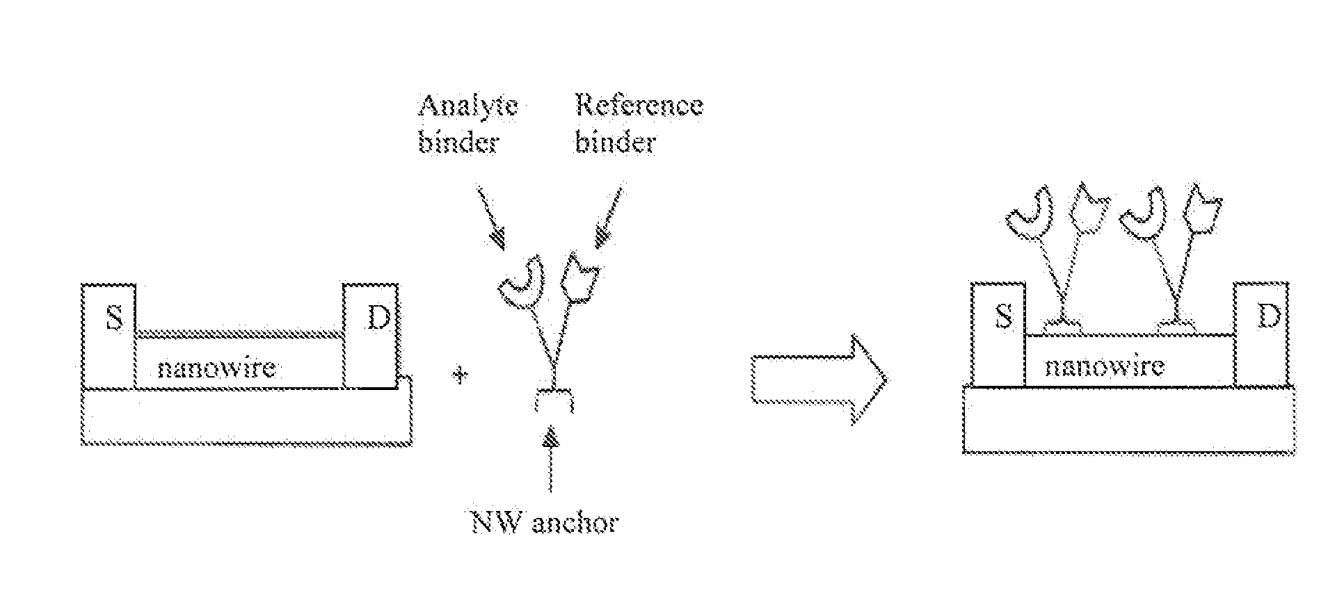
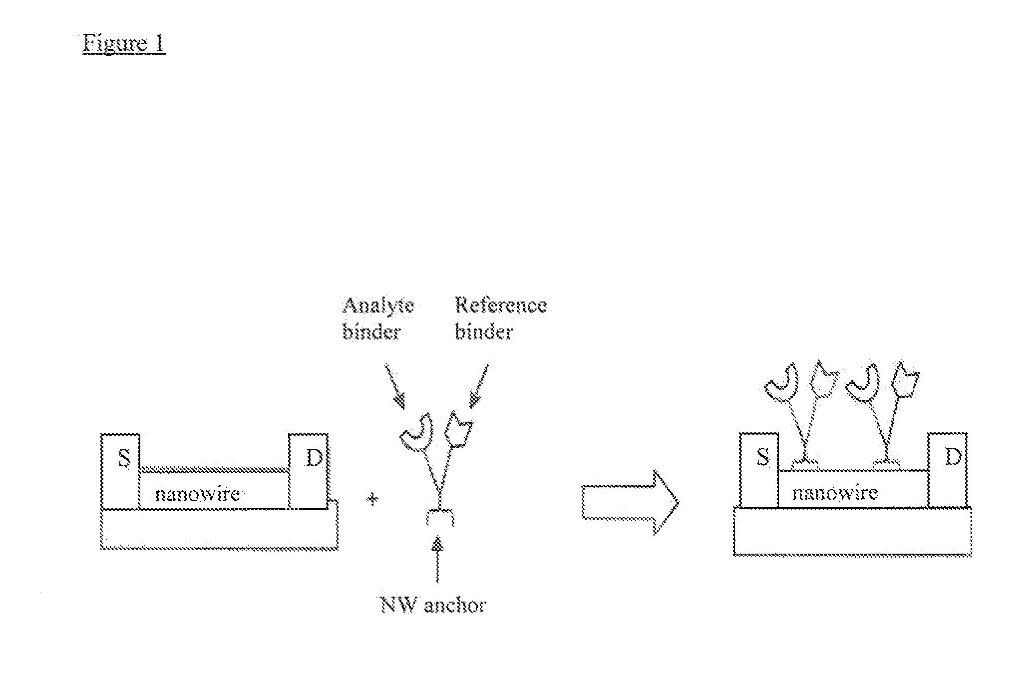
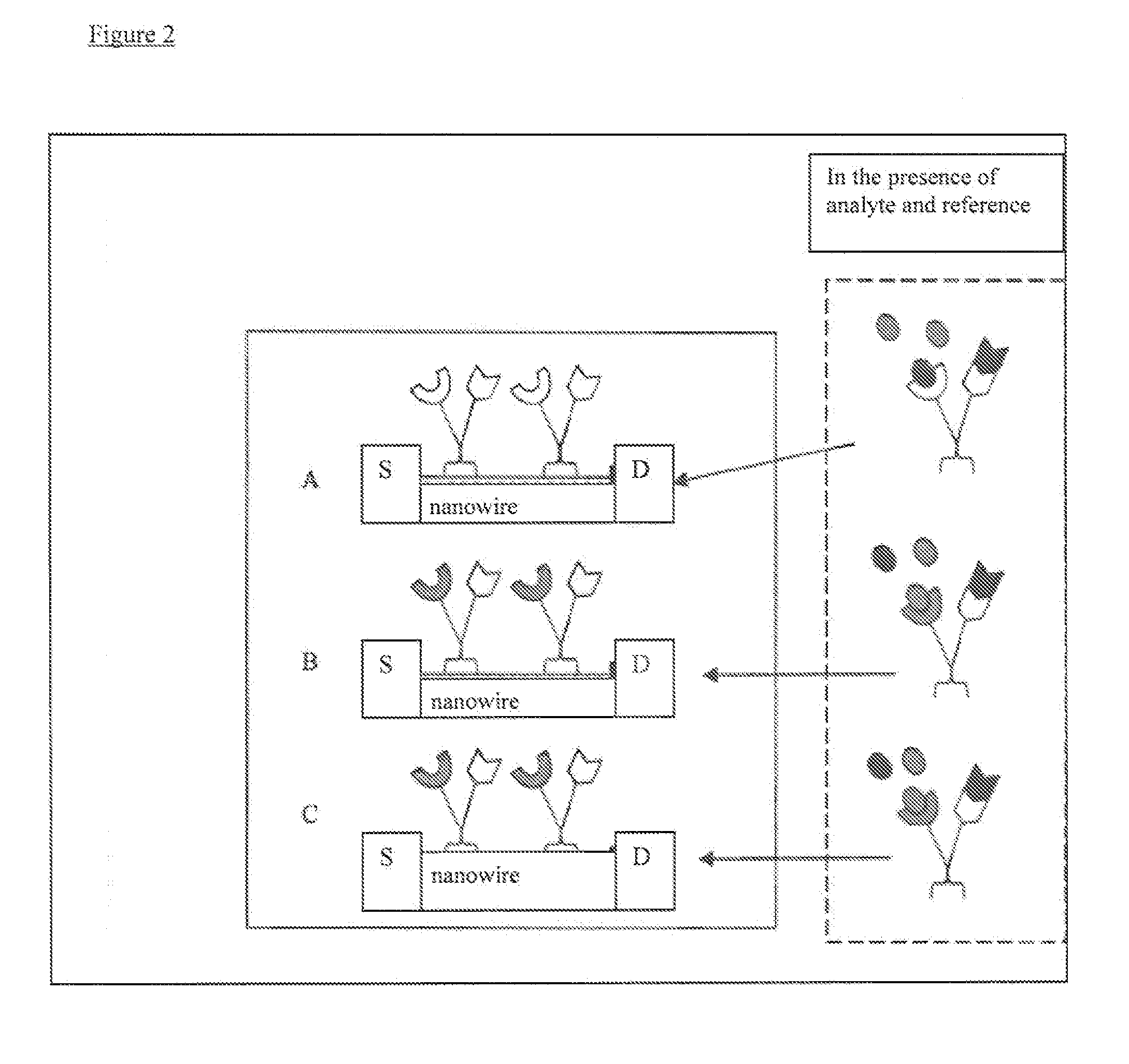
Calibration methods for multiplexed sensor arrays
PatentInactiveUS20100204062A1
Innovation
- The implementation of a method involving analyte and reference binders attached to nanosensors, where a calibration curve is generated using a reference material to correct for device variation, utilizing high-affinity pairs like biotin-avidin, allowing all devices in an array to respond to a common reference compound while detecting different analytes.
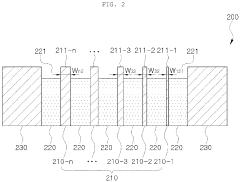
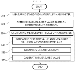
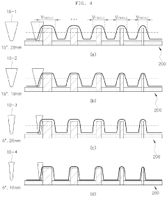
Method for calibrating NANO measurement scale and standard material used therein
PatentPendingEP4016090A1
Innovation
- A method involving a standard material with a series of nanostructures of certified values of different sizes, alternately stacked with intermediate layers, is used to calibrate the microscope measurement scale by measuring widths and determining deviations, allowing for linear fitting and calibration of measured values to align with certified values.
Manufacturing Standards for Nanosheet Devices
Manufacturing standards for nanosheet devices represent a critical framework that ensures consistent production quality, performance reliability, and scalability across different fabrication facilities. These standards encompass dimensional tolerances, material specifications, process control parameters, and quality assurance protocols specifically tailored to the unique characteristics of nanosheet transistor architectures.
The dimensional specifications for nanosheet devices require unprecedented precision control, with thickness variations typically maintained within ±0.5 nanometers for individual nanosheets. Width uniformity standards mandate less than 3% variation across arrays, while length specifications allow maximum deviations of ±2 nanometers. These tight tolerances are essential for maintaining consistent electrical characteristics and enabling effective calibration procedures across large-scale arrays.
Material purity standards for nanosheet fabrication exceed conventional semiconductor requirements, with metallic impurity concentrations limited to parts-per-billion levels. Silicon-germanium composition ratios must be controlled within ±0.1% for heterostructure nanosheets, while interface roughness specifications require root-mean-square values below 0.3 nanometers. These stringent material standards directly impact device performance uniformity and calibration accuracy.
Process control standards encompass critical manufacturing steps including epitaxial growth, lithography, etching, and gate formation. Temperature uniformity during epitaxial deposition must be maintained within ±1°C across wafer surfaces, while etch selectivity ratios require minimum values of 50:1 for sacrificial layer removal. Gate workfunction uniformity standards specify maximum variations of ±10 millivolts equivalent across device arrays.
Quality assurance protocols mandate comprehensive electrical testing at multiple manufacturing stages, including sheet resistance measurements with ±2% accuracy requirements and threshold voltage distributions within ±15 millivolts. Statistical process control implementation requires real-time monitoring of key parameters with automatic feedback mechanisms to maintain manufacturing consistency and support subsequent calibration optimization efforts.
Yield Optimization Strategies for Calibrated Arrays
Yield optimization for calibrated nanosheet transistor arrays represents a critical manufacturing imperative that directly impacts commercial viability and production economics. The inherent variability in nanosheet fabrication processes, combined with the precision requirements of calibration systems, creates unique challenges for achieving acceptable yield rates in large-scale production environments.
Statistical process control emerges as a fundamental strategy for yield enhancement, requiring comprehensive monitoring of key fabrication parameters throughout the manufacturing flow. Process variation reduction techniques focus on minimizing dimensional fluctuations in nanosheet thickness, width, and channel length, which directly correlate with transistor performance uniformity. Advanced metrology systems enable real-time feedback control, allowing for immediate process adjustments when parameters drift beyond acceptable tolerances.
Redundancy-based design approaches offer significant yield improvement potential by incorporating spare transistors and reconfigurable array architectures. These strategies enable functional arrays even when individual transistors fail post-calibration, effectively transforming hard failures into manageable performance variations. Adaptive calibration algorithms can dynamically exclude defective elements while redistributing functionality across remaining operational transistors.
Predictive yield modeling utilizes machine learning algorithms to identify process conditions most likely to produce high-yield wafers. These models incorporate historical fabrication data, inline metrology measurements, and post-calibration performance metrics to optimize process recipes proactively. Early detection of yield-limiting factors enables preventive interventions before defects propagate through subsequent processing steps.
Selective calibration strategies represent an emerging approach where only transistors meeting specific performance criteria undergo full calibration procedures. This methodology reduces calibration-induced stress and potential reliability degradation while maintaining overall array functionality. Hierarchical calibration schemes prioritize critical array regions, ensuring optimal performance where most needed while accepting relaxed specifications in less critical areas.
Post-fabrication repair techniques, including laser annealing and localized doping adjustments, provide additional yield recovery opportunities for arrays exhibiting marginal performance after initial calibration. These interventions can rescue otherwise functional arrays that fall slightly outside specification limits, significantly improving overall manufacturing yield and economic returns.
Unlock deeper insights with Patsnap Eureka Quick Research — get a full tech report to explore trends and direct your research. Try now!
Generate Your Research Report Instantly with AI Agent
Supercharge your innovation with Patsnap Eureka AI Agent Platform!